Sélection de la langue

Search

Sommaire du brevet 2617505 

Énoncé de désistement de responsabilité concernant l'information provenant de tiers

Une partie des informations de ce site Web a été fournie par des sources externes. Le gouvernement du Canada n'assume aucune responsabilité concernant la précision, l'actualité ou la fiabilité des informations fournies par les sources externes. Les utilisateurs qui désirent employer cette information devraient consulter directement la source des informations. Le contenu fourni par les sources externes n'est pas assujetti aux exigences sur les langues officielles, la protection des renseignements personnels et l'accessibilité.

Disponibilité de l'Abrégé et des Revendications

L'apparition de différences dans le texte et l'image des Revendications et de l'Abrégé dépend du moment auquel le document est publié. Les textes des Revendications et de l'Abrégé sont affichés :

  • lorsque la demande peut être examinée par le public;
  • lorsque le brevet est émis (délivrance).
(12) Brevet: (11) CA 2617505
(54) Titre français: RESISTANCE TERMINALE HF PRESENTANT UNE STRUCTURE DE COUCHES PLANE
(54) Titre anglais: HF TERMINATING RESISTOR HAVING A PLANAR LAYER STRUCTURE
Statut: Accordé et délivré
Données bibliographiques
(51) Classification internationale des brevets (CIB):
  • H01C 01/14 (2006.01)
  • H01C 07/00 (2006.01)
  • H01P 01/26 (2006.01)
(72) Inventeurs :
  • WEISS, FRANK (Allemagne)
  • ZAHN, DIETRICH (Allemagne)
(73) Titulaires :
  • ROSENBERGER HOCHFREQUENZTECHNIK GMBH & CO. KG
(71) Demandeurs :
  • ROSENBERGER HOCHFREQUENZTECHNIK GMBH & CO. KG (Allemagne)
(74) Agent: SMART & BIGGAR LP
(74) Co-agent:
(45) Délivré: 2014-10-07
(86) Date de dépôt PCT: 2006-08-16
(87) Mise à la disponibilité du public: 2007-03-01
Requête d'examen: 2011-07-22
Licence disponible: S.O.
Cédé au domaine public: S.O.
(25) Langue des documents déposés: Anglais

Traité de coopération en matière de brevets (PCT): Oui
(86) Numéro de la demande PCT: PCT/EP2006/008089
(87) Numéro de publication internationale PCT: EP2006008089
(85) Entrée nationale: 2008-01-31

(30) Données de priorité de la demande:
Numéro de la demande Pays / territoire Date
20 2005 013 515.1 (Allemagne) 2005-08-26

Abrégés

Abrégé français

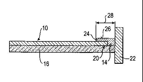
L'invention concerne une résistance terminale HF présentant une structure de couches plane, comportant sur un substrat (16) une couche de résistance (10) destinée à convertir de l'énergie HF en chaleur, une piste d'entrée (12) destinée à l'alimentation en énergie HF, et une piste de connexion de masse (14) destinée à la connexion électrique avec un contact de masse (22). La piste d'entrée (12) est connectée électriquement à une première extrémité (18) de la couche de résistance (10) et la piste de connexion de masse (14) est connectée électriquement à une deuxième extrémité (20) de la couche de résistance (10), opposée à la première (18). Sur une extrémité côté contact de masse de la structure de couches, la piste de connexion de masse (14) forme la couche supérieure de la structure de couches. La piste de connexion de masse (14) est au moins partiellement disposée sur la couche de résistance (10).


Abrégé anglais


The invention relates to an HF terminating resistor having a planar layer
structure which, on a substrate (16), comprises a resistor layer (10) for
converting HF energy to heat, an input conductor (12) for supplying HF energy
and an earthing conductor (14) for the electric connection to an earthing
contact (22). The input conductor (12) is electrically connected to a first
end (18) of the resistor layer (10) and the earthing conductor (14) is
electrically connected to a second end (20) of the resistor layer (10)
opposite the first end (18). On an earthing contact end of the layer
structure, the earthing conductor (14) forms the topmost layer of the layer
structure. The invention is characterized in that the earthing conductor (14)
is at least partially arranged on the resistor layer (10).

Revendications

Note : Les revendications sont présentées dans la langue officielle dans laquelle elles ont été soumises.


Claims:
1. An HF terminating resistor having a planar layer structure which, on a
substrate, comprises a resistor layer for converting HF energy to heat, an
input
conductor for supplying HF energy and an earthing conductor for the electric
connection to an earthing contact where the earthing contact is arranged on an
end
face of the planar layer structure on the earthing contact side, in which the
input
conductor is electrically connected to a first end of the resistor layer and
the
earthing conductor is electrically connected to a second end of the resistor
layer
opposite the first end, and on an earthing contact end of the layer structure,
the
earthing conductor forms the topmost layer of the layer structure,
characterized in
that the earthing conductor is at least partially arranged on the resistor
layer
extending parallel to and beyond said resistor layer second end.
2. The HF terminating resistor according to claim 1, including having the
planar
layer structure arranged in a housing of electrically conductive material,
with the
earthing contact being the housing.
3. The HF terminating resistor according to claim 1, wherein said earthing
conductor extends beyond both sides of said resistor layer in a direction
perpendicular to said resistor layer first end.
4. The HF terminating resistor according to claim 1, including at the end
of the
layer structure on the earthing contact side, the earthing conductor is
arranged on
the substrate and has a widened portion extending in the direction of the
first end
of the resistor layer, which portion is arranged on the resistor layer.
5. The HF terminating resistor according to claim 4, including having the
planar
layer structure arranged in a housing of electrically conductive material,
with the
earthing contact being the housing.
6. The HF terminating resistor according to claim 4, including having the
earthing contact arranged on an end face of the planar layer structure on the
earthing contact side.
6

7. The HF terminating resistor according to claim 4, including having an
upper
side of the earthing conductor facing away from the substrate extending in an
area
both in the region of the end of the layer structure on the earthing contact
side, in
which the earthing conductor lies on the substrate and also in the region of
the
widened portion, in which the earthing conductor lies on the resistor layer.
8. The HF terminating resistor according to claim 7, including having the
planar
layer structure arranged in a housing of electrically conductive material,
with the
earthing contact being the housing.
9. A method for the production of a planar layer structure for an HF
terminating
resistor comprising a resistor layer for converting HF energy to heat, an
input
conductor for supplying HF energy and an earthing conductor for the electric
connection to an earthing contact is formed on a substrate, in which the input
conductor is electrically connected to a first end of the resistor layer and
the
earthing conductor is electrically connected to a second end of the resistor
layer
opposite the first end, including having the resistor layer firstly formed on
the
substrate and thereafter the earthing conductor formed at least partially on
the
resistor layer and extending parallel to and beyond said resistor layer second
end.
7

Description

Note : Les descriptions sont présentées dans la langue officielle dans laquelle elles ont été soumises.


CA 02617505 2008-01-31
WO 2007/022906 A2
HF Terminating Resistor having a Planar LayerStructure
The present invention relates to an HF terminating resistor having a planar
layer structure
which, on a substrate, comprises a resistor layer for converting HF energy to
heat, an input
conductor for supplying HF energy and an earthing conductor for the electric
connection to an
earthing contact, in which the input conductor is electrically connected to a
first end of the
resistor layer and the earthing conductor is electrically connected to a
second end of the resistor
layer opposite the first end, and on an earthing contact end of the layer
structure, the earthing
conductor forms the topmost layer of the layer structure, according to the
introductory clause of
Claim 1. The invention further relates to a method for producing a planar
layer structure for an
HF terminating resistor, in which on a substrate a resistor layer is formed
for converting HF
energy to heat, an input conductor for supplying HF energy and an earthing
conductor for the
electric connection to an earthing contact, in which the input conductor is
electrically connected
to a first end of the resistor layer and the earthing conductor is
electrically connected to a
second end of the resistor layer opposite the first end, according to the
introductory clause of
Claim 6.
HF terminating resistors are used for example for matching HF assemblies in
the mobile- and
radio link field with very high transmitting power, e.g. to terminate a
combiner or antenna output.
Terminating resistors of increased power loss have large resistance structures
in order to
distribute the coupled-in HF power to this area. However, this has an
unfavourable effect on the
reflection factor in broadband application, or the terminating resistor is
only able to be used in a
narrower frequency band with the same reflection factors.
In the above-mentioned HF terminating resistors, special constructions of the
substrate
structures are necessary in order, through these, to meet the very high
technical requirements.
The invention is based on the problem of developing an HF terminating resistor
of the above-
mentioned type and a method of the above-mentioned type in such a way that the
earthing
connection of the resistor structure of the substrate to the earthing contact,
such as for example
a housing wall, is on the one hand very short, in order to obtain as precise a
matching as
possible of the wave resistance, but on the other hand is constructed so that
a good solder joint
can still form for the earthing contact between the earthing conductor and the
earthing contact.
This problem is solved according to the invention by an HF terminating
resistor of the above-
mentioned type with the features characterized in Claim 1 and by a method of
the above-

CA 02617505 2008-01-31
2
mentioned type with the features characterized in Claim 6. Advantageous
developments of the
invention are described in the further claims.
In an HF terminating resistor of the above-mentioned type, provision is made
according to the
invention that the earthing conductor is at least partially arranged on the
resistor layer.
In a method of the above-mentioned type, provision is made according to the
invention that
firstly the resistor layer is formed on the substrate and thereafter the
earthing conductor is
formed at least partially on the resistor layer.
This has the advantage that the upper side of the earthing conductorJies
completely free and is
thereby fully available for the contacting with the earthing contact. Hereby,
it is possible to form
the earthing conductor to be as short as necessary for a sufficient electrical
connection with the
earthing contact, so that the negative electrical effects of the earthing
connection on the
matching of the wave resistance of the HF terminating resistor can be
minimized and at the
same time the surface which is available for the electrical contacting can be
maximized.
In a preferred embodiment, the earthing conductor is arranged on the substrate
on an earthing
contact end of the layer structure, and has a widened portion extending
towards the first end of
the resistor layer, this widened portion being arranged on the resistor layer.
A good electrical contacting, able to be produced in a functionally reliable
way, between the
earthing conductor and the earthing contact is achieved in that an upper side
of the earthing
conductor facing away from the substrate extends in an area both in the region
of the end of the
layer structure on the earthing contact side in which the earthing conductor
lies on the
substrate, and also in the region of the widened portion in which the earthing
conductor lies on
the resistor layer.
To carry off the heat generated in the resistor layer, the planar layer
structure is arranged in a
housing of electrically conductive material, with the earthing contact being
the housing.
Expediently, the earthing contact is arranged on an end face of the planar
layer structure on the
earthing contact side.
The invention is explained in further detail below with the aid of the
drawings, in which:

CA 02617505 2008-01-31
3
Fig. 1 shows a preferred embodiment of an HF terminating resistor according to
the invention,
in top view;
Fig. 2 shows the HF terminating resistor of Fig. 1 in diagrammatic sectional
view;
Fig. 3 shows a graphical illustration of the matching of the wave resistance
over the frequency
for a length of the earthing conductor of L = 0.6 mm; and
Fig. 4 shows a graphical illustration of the matching of the.wave resistance
over the frequency
for a length of the earthing conductor of L = 1.1 mm.
The preferred embodiment, which can be seen from Fig. 1, of an HF terminating
resistor
according to the invention comprises a resistor layer 10, an input conductor
12 and an earthing
conductor 14. The resistor layer 10, the input conductor 12 and the earthing
conductor 14 are
formed as respective layers on a substrate 16 and form a planar layer
structure. The input
conductor 12 is electrically connected to a first end 18 of the resistor layer
10, and the earthing
conductor 14 is electrically connected with a second end 20 of the resistor
layer 10 opposite the
first end 18. The resistor layer 10 serves to convert HF energy to heat, the
input conductor 12
serves to supply HG energy, and the earthing conductor 14 serves for
electrical connection to
an earthing contact 22 (Fig. 2).
The planar layer structure, formed by the input conductor 12 (not illustrated
in Fig. 2), the
resistor layer 10 and the earthing conductor 14 can be seen in further detail
from Fig. 2. The
earthing contact 22 is arranged on the end face on an end of the layer
structure on the earthing
contact side, and is a part of a housing, for example. This housing is made
from an electrically
conductive material and thereby also has good heat-conducting properties, so
that the thermal
energy occurring in the resistor layer 10 is carried off to a cooling body via
the housing.
The earthing conductor 14 produces the electrical contact between the resistor
layer 10 and the
housing 22. According to the invention, the earthing conductor 14 is arranged
at least partially
on the resistor layer 10. At the end of the layer structure on the earthing
contact side, the
earthing conductor 14 is arranged on the substrate 16. A widened portion 24 of
the earthing
conductor 14 which is arranged on the resistor layer 10 extends in the
direction of the first end
18 of the resistor layer 10, i.e. the resistor layer 10 is arranged in the
region of the widened
portion 24 between the substrate 16 and the earthing conductor 14.

CA 02617505 2008-01-31
4
An upper side 26 of the earthing conductor 14, facing away from the substrate
16, extends in an
area both in the region of the end of the layer structure on the earthing
contact side, in which
the earthing conductor 14 lies on the substrate 16, and also in the region of
the widened portion
24, in which the earthing conductor 14 lies on the resistor layer 10. This
flat upper side 26 of the
earthing conductor 14 serves to provide the electrical contact with the
housing 22, in which
preferably a soldered joint is produced. To do this, a length 28 of the
earthing conductor 14, i.e.
an extent of the earthing conductor 14 in the propagation direction of the HF
wave, must have a
minimum length because otherwise a sufficient solder fillet can not form. On
the other hand,
negative effects occur all the greater on the impedance matching, the greater
the value for the
length 28. Through the fact that the earthing conductor 14 at the end of the
layer structure on
the earthing contact side also constitutes the topmost layer in the region of
the overlap with the
resistor layer 10, this length 28 can be selected to be as small as is
absolutely necessary for
contacting with the housing. The negative influence of the earthing conductor
14 on the
impedance matching of the HF terminating resistor is thereby minimized.
A short geometric distance is necessary between the second end 20 of the
resistor layer 10 and
the housing wall 22. At the same time, the technological requirement exists
for a sufficient
length 28 of the soldered joint and for a favourably priced construction. All
requirements are met
by the layer structure according to the invention (earthing conductor 14 on
resistor layer 10). A
simple, favourably priced construction is produced (no front face contacting),
a sufficient
soldering surface for a uniform, clean soldered joint (earthing connection to
the housing 22,
which ensures a fillet formation), and despite large resistance structures one
has a contact point
for optimizing the reflection factor, because the length 28 of the earthing
conductor 14 has a
crucial influence on the electrical parameters. The illustrated favourably-
priced manufacturing
technology for planar structures has a very advantageous effect on the HF
properties.
A method for producing a planar layer structure for an HF terminating
resistor, in which a
resistor layer for converting HF energy to heat, an input conductor for
supplying HF energy and
an earthing conductor for electrical connection to an earthing contact is
formed on a substrate,
in which the input conductor is electrically connected to a first end of the
resistor layer and the
earthing conductor is electrically connected to a second end of the resistor
layer opposite the
first end, is characterized in that firstly the resistor layer is formed on
the substrate and
thereafter the earthing conductor is formed at least partially on the resistor
layer.
The influence of the length L 28 of the earthing conductor 14 is shown in Fig.
3 and 4. In Fig. 3
the impedance matching is indicated over the frequency for L = 0.6 mm and in
Fig. 4 the
impedance matching is indicated over the frequency for L = 1.1 mm. As can be
immediately

CA 02617505 2008-01-31
seen, in the range of 0.50 GHz to 2.00 GHz an impedance matching which is
better by
approximately 4 dB is produced for length 28 L 0.6 (Fig. 3).

Dessin représentatif
Une figure unique qui représente un dessin illustrant l'invention.
États administratifs

2024-08-01 : Dans le cadre de la transition vers les Brevets de nouvelle génération (BNG), la base de données sur les brevets canadiens (BDBC) contient désormais un Historique d'événement plus détaillé, qui reproduit le Journal des événements de notre nouvelle solution interne.

Veuillez noter que les événements débutant par « Inactive : » se réfèrent à des événements qui ne sont plus utilisés dans notre nouvelle solution interne.

Pour une meilleure compréhension de l'état de la demande ou brevet qui figure sur cette page, la rubrique Mise en garde , et les descriptions de Brevet , Historique d'événement , Taxes périodiques et Historique des paiements devraient être consultées.

Historique d'événement

Description Date
Paiement d'une taxe pour le maintien en état jugé conforme 2024-07-30
Requête visant le maintien en état reçue 2024-07-30
Représentant commun nommé 2019-10-30
Requête pour le changement d'adresse ou de mode de correspondance reçue 2018-01-12
Accordé par délivrance 2014-10-07
Inactive : Page couverture publiée 2014-10-06
Préoctroi 2014-06-16
Inactive : Taxe finale reçue 2014-06-16
Un avis d'acceptation est envoyé 2014-04-22
Lettre envoyée 2014-04-22
Un avis d'acceptation est envoyé 2014-04-22
Inactive : Approuvée aux fins d'acceptation (AFA) 2014-04-08
Inactive : Q2 réussi 2014-04-08
Modification reçue - modification volontaire 2013-05-23
Inactive : Dem. de l'examinateur par.30(2) Règles 2012-11-28
Lettre envoyée 2011-08-09
Requête d'examen reçue 2011-07-22
Exigences pour une requête d'examen - jugée conforme 2011-07-22
Toutes les exigences pour l'examen - jugée conforme 2011-07-22
Inactive : Page couverture publiée 2008-04-24
Inactive : Notice - Entrée phase nat. - Pas de RE 2008-04-21
Inactive : CIB en 1re position 2008-02-22
Demande reçue - PCT 2008-02-21
Exigences pour l'entrée dans la phase nationale - jugée conforme 2008-01-31
Demande publiée (accessible au public) 2007-03-01

Historique d'abandonnement

Il n'y a pas d'historique d'abandonnement

Taxes périodiques

Le dernier paiement a été reçu le 2014-08-05

Avis : Si le paiement en totalité n'a pas été reçu au plus tard à la date indiquée, une taxe supplémentaire peut être imposée, soit une des taxes suivantes :

  • taxe de rétablissement ;
  • taxe pour paiement en souffrance ; ou
  • taxe additionnelle pour le renversement d'une péremption réputée.

Les taxes sur les brevets sont ajustées au 1er janvier de chaque année. Les montants ci-dessus sont les montants actuels s'ils sont reçus au plus tard le 31 décembre de l'année en cours.
Veuillez vous référer à la page web des taxes sur les brevets de l'OPIC pour voir tous les montants actuels des taxes.

Titulaires au dossier

Les titulaires actuels et antérieures au dossier sont affichés en ordre alphabétique.

Titulaires actuels au dossier
ROSENBERGER HOCHFREQUENZTECHNIK GMBH & CO. KG
Titulaires antérieures au dossier
DIETRICH ZAHN
FRANK WEISS
Les propriétaires antérieurs qui ne figurent pas dans la liste des « Propriétaires au dossier » apparaîtront dans d'autres documents au dossier.
Documents

Pour visionner les fichiers sélectionnés, entrer le code reCAPTCHA :


Pour visualiser une image, cliquer sur un lien dans la colonne description du document. Pour télécharger l'image (les images), cliquer l'une ou plusieurs cases à cocher dans la première colonne et ensuite cliquer sur le bouton "Télécharger sélection en format PDF (archive Zip)" ou le bouton "Télécharger sélection (en un fichier PDF fusionné)".

Liste des documents de brevet publiés et non publiés sur la BDBC .

Si vous avez des difficultés à accéder au contenu, veuillez communiquer avec le Centre de services à la clientèle au 1-866-997-1936, ou envoyer un courriel au Centre de service à la clientèle de l'OPIC.


Description du
Document 
Date
(aaaa-mm-jj) 
Nombre de pages   Taille de l'image (Ko) 
Abrégé 2008-01-30 2 95
Dessin représentatif 2008-01-30 1 7
Revendications 2008-01-30 2 57
Dessins 2008-01-30 2 29
Description 2008-01-30 5 219
Revendications 2013-05-22 2 74
Dessin représentatif 2014-09-04 1 9
Confirmation de soumission électronique 2024-07-29 2 71
Avis d'entree dans la phase nationale 2008-04-20 1 195
Rappel de taxe de maintien due 2008-04-20 1 114
Rappel - requête d'examen 2011-04-18 1 119
Accusé de réception de la requête d'examen 2011-08-08 1 177
Avis du commissaire - Demande jugée acceptable 2014-04-21 1 161
PCT 2008-01-30 2 69
Taxes 2008-07-30 1 37
Taxes 2009-07-30 1 36
Taxes 2010-08-02 1 36
Correspondance 2014-06-15 1 53