Note : Les descriptions sont présentées dans la langue officielle dans laquelle elles ont été soumises.
CA 02621665 2008-02-15
T,ansparent andior P!hotcvoltaic Solar Cell ana hM1odule
Fieid of the lnvention
The present invention relates to design and tabrication of solar celis and
modu!es.
ac ound oi the invention
The bulk of today's photovoltaic solar panel sales are integrated to ho.ases
ta minirnize system cost, minimize iand use, and also for architectural
reasons.
A!thougn in most cases solar paneis are installed on the roof, It is also
possible to
use the in0;,xiow space ard skylight for this purpose.
Ivlore Lhan 90% of photovoitaic panels (soid and installed) are based on
crystalline {mono and polycrystalline) silicon, For aestnetic and for
budgeting
reasons, crystalline baseC soisr oelis are probably rot the most suitable
photovcltaic teehnology. For this reason var9ous thin film based photovoltaic
paneis are expec*.sd to overtake crystalline siiicon as the dominant
technology in
the future For example, thLn film technology uses less than two orders of
magnitude less photovoltaic material, and the process of fabrication is
simpier.
rhers are two major drawbacks wtien using thin film technclogy to fabricate
photovoltac solar panels. First, expensive equipment is required. Indeed
uriform
and large area coating requires large vacuum sur,tems with muiti-stap slow
deposition rates. Second, power efficiency of commercial photovoltaic panels
are
stil 30-50% lower than their crystalline silicon counterparts.
There are few examples in the Iiterature of using non-vacuurn processes to
faoricate solar panels. Sc far the efficiencies achievea are at least 50'/o
lo+rjer
than cry5ta7ire based saiar oanel.
Nanostructured hybrid materials have beer used in several sclar cell
designs. For example, nanoparticles ernhadded in conductive polymer matrix
provide power efficiency of about 3% at labora:ory scale. fv?odified Cso
molecules
can be =nixed with conductlve polymers to form a nanooomposite witfi slightly
higher power efficiency.
1
CA 02621665 2008-02-15
Althougf? tt=cy,;e rnatc-.nai, are iajaa{ ;r, maximize solar light absorption,
excitor caener=G:tirx; ard 1--il separa;iryn, oftc;r charge coll?ctior ray top
and
i;n*orn electrodes s ve y lirnited, lnrleed the junction does not provide
efficient
r:h4r7s trenspor towerci ae.t'. I elertredes after e*ctron and hole ere
separated. In
parFic,u"ar. charge transfer treMEari nercpFrtici<,s or between Gan
rr:olc:cuEes ;s
?ne;tcient. To mitigate thai, high nanoparti".1e cr modified Gw oadin,,re is
requred.
'"'iere re!^nains a naed #or ;rrsproved solar cell and solar nioduls design.
,S t^ r^an of #I~~ Inventi~!?.
rhere is proviryer5 a sciar celi conrprising a first a'ectrlcali;v conr+uctive
iayer,
Ir3 a second electricadly corductive iayer, an n-type semiconductor layer and
a p-type
sarriconauci.or layer, the fZ-t.ype and p-type serr;icnnductor layers forrning
a
ju^ct;on, the secnicnnducmr ;ayers comprising nanoparticulrate semkonductor
rnaterial, end ar ieast one of the eisctr'.c&ly conductive !ayers having a
pattern
form,;ng a iliree=din9.;~n:,ione.3 ~eiigr.
There is further pr:;videj a solar n?o:luie cornorising a soiar call of the
uresent invent!on.
' he,e is yet further p rovidac a process for fabricating a sotar ce!l
comprising pE+uviP,;ny a frrst eier,iriually conductive layer, providirg a
second
eiectri ,a ly condur":ive ayer, pavern!ng eitner cr both of tne first andPrar
second
elactriaaiiy ca^nduc:~ve 4aa+ers witrr one or m,ore pre-determined pattenis
forming a
three-d,msnslo^ai rerief, prowidirra arr n-type semiconductor fayer
ccrnprising
n ancpar:iculate semiconducior materiai ~cn one of the electrically concuJtive
layars, prz:vidin~.^i s p4Eyps sen;;conductor layer= cornpri:s9;1g
nancparticulate
:-amicondu;a:tor material on the otr~er of the eledricaily cr?ndcctive layers,
and
ferminc fhe solar cell by brincaing the n-tyr.ye semiconductar iayer intu
contact with
the põtype s9rn's;cnduct-Afa>rer.
The sc;sar ciA nray further ccmpriss ona or more transparent sut-strate.s to
pr;.vide protvctiux, for thC a)rprs arld to perrnit easier i`kanul'iny of the
cell. A
transparord ~sucr;:trate rrrGiy coa-;prise, for r~xarnfa!o. glass, plastic,
etc. Transparent
3 D ~"ubs#.ratas preferab!y r5avc a thickness of 1 iram or crreater, more
preferabiy fxrn
2
CA 02621665 2008-02-15
atnoõ,t "mm to about 70 rr-irn, for exarnple about 3 rrur. Preferably, the
solar cail is
csonsfructed with two transparerrt sunsirates, other layers being dispcsed
cetween
the tw substrates.
Or,a or rr,Grs ;:urrant c:ollector kwyers, for ex2rnpip rnEtai strps anTor
grids,
mray t~~~e inciuc+ed tc a.c: as c.rrrer;t ,crliecto-s. C=urrerrt collector
4oyers are
f::referal7hy formed cn the transparent .:ukr.strates between the substrates
arrd other
layers oT the solar ce!!. Currarrt cailector layers preferably cornprise a
high
crsnductiv!iy matal for exampRr= si!ver, aluminum, rticiceS, er a mixt;.re
thereof.
t:;u; rer,t coiivct.or ia, ar:_a are p^efe^abiy about 1.00 {:rn 'thick.
One or mor-barrier Msiyers may also 45 included to separate a sutrsstrate or
substraaas from the other layers of the sclar :el!. A barrier layer preferably
ct,rnpriMes silicon dicxfd.a cr poly(;3,4 ethylenedioxythiophene}
no9y(st ~r4~id asuifonate) ;f'Ft~ a?':PSB;. Barrier iayers are pretera'uly
thin,
pr;fersbly having a thickness :,f from about 0.1 pm to abcut I iam.
5 "1'he; 4lectrical6y corr~;uctiue ab~er s may corr prise, for example,
rrratalfic
rõrtertsl, transparertt conductive materials, or combinaticns thereof.
tronci.cr:rve
'ayers are creferabl,y tliln Pllms, praferabhy having a thickness of aaout 5
prn or
Icss, more preferably about 2 pm or less, ror sxamPle aboui I pn;. A givan
condurtiva iayer may comrrise one r,r more thin `iints. Preferably. at feaGt
one of
i.ne ,;ondl.active lay6rs cornprises a fiin? oF transparQr-!t conductive
rraterial.
7rrrsparpnt c.crnrluctive materi;.~fs are Nret'erahiy tr.nsoarent cc,nductlve
oxides
fcr example indiurn-tin oxide (iT'a"?), Zr~,0, ZnaAl, SnO? and Sn02:d=.
YrFwWf;arent conouctive rr,aterEa;s are preferably chcaer-r to pravde high
transparency and imY "`e:'ai,`~i'CEV~iy. .k`atallic matc:riais !noiUde, tDr
example, gold.
~.'5 aium,nunn, sihw, rnoiyW srourn. etc. 'vlc:ly'adenum rs rnore suitabie to
ba.=it a p-
type se:micond::cto- ;ay+s: vahi9a <alurnirn r7 and silver are rnr,re
suitapir3 fr,r an n-
tyNe sarriicur.ductor layer. +Nhen a oondu=:tive la;yer is a jusi a flrn of
rnetaiiic
rr7~t~rial, i=re fiir-r prefr+robly has a thicicness cf !e+ss -than about I
Pm, pmferabiy
at'out 250-7-,.0 nr,=rr, for example abaut 500 nrn
One or more of :ne rxlorluctive layers have a pattern forrning a three-
dirr:a,nsional raRie3s. The FYr=: :ern i:,referably covers mnst or all of nne
surface af the
3
CA 02621665 2008-02-15
c-c,nuzic.tive Iayer tr> fr,rr,t e par:erned conductive iayer. Preferably, aq
of the
cx}nOuc:ive layers have a pattem. The patterned conductive layer prefErabig
cX?rriw r! rt3s 8"".fJft pe,t!erried p=Ortlcn ffitl'.i a!JK'tfArned porC;on,
the patterned portlo=n
bei,ica ?rti con:atYt wi," ; s^4m c,ondu:tor iayer. `I-he catterled por[IQri
may be
w tqraS with the raon-pat7ernr>d pa tEor; -~;rrning the t! =ree-dimr~nsion
re!it f on tt~ie
ncn=.,p~~ternar:i p~ji1;iUjy, eDr tr?e patterned ar-itf non-patterned
pc;r:icns may be
ser.arate'rilros ir, cvtt-aci wiih each oYhÃwr.
In one 4rnboriir",ent, a rznductive layer may romprise an ultrrathin metal,ic
f'ilrn and a 1'llni ol- t.rnnsparert conduCi?ve 'naterta9. The uitmathlYi
meta9llc fiim
prefersbly has a thick.n!?es ot cxbout 10=200 f!rn, for exarnple about 20 nm.
The
fili?7 of ~rsnsparent >=~onduotive ma:eri:>:si would be patterned but
cont!riuity be;ween
pari:ern sPer=i4nts of tre ftlrn wr,uid noi h-a required.
ir. a preterre;l er~rbodÃrnent, one or mcre .f the coriductive iayers is a
filrrr of
transparent conduUti~,rcA materiafs in which the patternec: portion Is
integraf!}r
?S '.;,rmed with the non-naxterned paftian. irr this embodirnent, the
patterned portion
10rrnw a:;~rea-ui n~~nsinnaf re;ie4 on t1e non-,.atterned partion and the non-
pe tprne~ cor" cen has a thickness that ar`fords'ow she+et a!ectncai
resistance ia=;
about ^..2r3 ohrrr!cr-z`,'er r;xampAe about 10 ohrntcrn21 with hig;;
transmission (e.g.
at7,)ut 50-98% fo- exarnpis about 90gfo) }n the v!sl+a:e and nGar i:?ta"ed
reglon3 Cf
2 6, the ei?ctrUrT.aqnetlc s"}3eK.'~'=iJri'k.
Patterning of the corductivf: layer or iQyers provides a high aspect ratio
ftrr
+..~ne or bor'i of these layers arrd +or the one or trnth of the
serniconductor layers
c::.,ated tharaan. High aspect ratio ~ensds to better photovo!tnic g5nerati;;n
wnile
!:flirsr.i able to keep ths Ãaye.rs triinrer. Thus, surfa.ce area contact
between the
25 ssrtliC:a.+n[1L'cto+" !^oyer or 1aye "s and the t;tlnf"t.tr,tlve layer c,"
layCsrs 's Iricreased
v:hile redu,--ir g .he volE~ntv Of rratvriais .r,sed in ;ne layers.
-iartherrn~re. by selecting pat~(Irn perameters !e,.j. distanoe between
patterrls, dis~.anrae bet4usen oattern efernenis, shiape of pattern
efenierats, dept!1 of
the Pa;.tem r~"#c.i it is pc;ssierlt, tn tt:rre a-id or optimize light
trgrsmiss"ion through
3i~ the cets, ph<utovoltalc power rF:neration andlor the balance between light
transrrriss,orr ar,d photcvoltaic power gene~atfori.
CA 02621665 2008-02-15
Pattern e,letnents in the patterned part preferably have a sl-,a.pe, siuc; an.-
I
s,aiJar=stiorr that optimir_a ovarail cell efficiency. Shapes inr!.jde, `or
example,
tslar,gr,lar shapes, rec.~tangwar sheapes, pen?agonr3i shapes, uurved shapes
(e.y.
+ bmispneres). a rdanrtular shapYd pat:ern e!ements are particulariy
praferrec. The
size at (he pattern eiornent5 is hrefera:slv aboui 0.1-5 Nm, tnr exarrpte
abcui 0.6
p3-t. ,Seoarati*n of ths pattern a9errtar;ts is preferabiy at?cjt ri prn or
mere, mom
praferabi.; about 2 tr5ir:rons or rr-,are, for example about 2-10 Firn.
T'o c:ust,7rnize or optimize light transrrission through the solar cell,
distance
and aspect ratio between patterned !ayers in the call may w a.djusted. For
euzmpie, to raatimize !ight transmrsion through the cefl, c!istartice
betweer=, tuw
sur`ace.s of the pa:torned iayars may ha srnaÃ4er thari trye wave!ength of
v!sible
iiot
"'"he semiconductor lay:rs may be very thin, preferably from aboit 1C~ nm to
abo-,ft 5 p:-rr t37ick. For the n-type serniconductor layer, the thickness is
rrtore
15 I:referablvtrnm abcut 100 nm ts; aboux 1 pm, for example about 500 nm. For
the
p-tyns sYmicor,duc;'or la}rer, the thickness is more preferably from about 50
nm to
a.b~.}:st 1prn, fcr exE mp'e about 200 nm. Coating a-:.emicorductor layer arP,
t:ie
patterned side of a patterned c-,onauczivo layer irnparts a complemeritary
pattern to
cne side af tha sernican" +uwtor ieyer
20 "CI-ro ;ae-miconductnr layars con?.pr se nanoparticuiate senii4:onductor
rr;atertal. Examples of suitable sernir,*nductor materials are given in
comrnon,y
,:vdrred PC7' app!lcatfon PCT/0A2006=11?2 fiiled July 11, 2006. For exGrnpie,
semicorductor matrsrials may comprise CdS, GaS, ZnS. CdSe, GeSe. ZnSe
CdTE, GaTe, SIC, Si, CIS, GaAs, PbS, PbSe. Culnae2, CUlnv2!, C'utlnGa)(S,Se)2:
25 oha{;opyri!e, pe:iy(3-hexvfth6ochene) (P3H't), poiyi2-methoxy-5-(2'-ethyl-
fi 2xyir x,1.1,~-phenylFr~z "Jnyienej SIVrH-r''PV), [6,6]-ishenyl.C-batyric
aciu rnethy{
ester (PucN,l), cr a mixture thereof Band gap for the semicorfductors is
E;refer,-~jbfy less than about 1.8 eV, fer examale l.ess than about 1.5 eV,
for
~..;:rn41e':sss than 1.3 FV. More pr=ferataly the band gap is in a range of
about
30 1.1-1.3 eV, for ex.arr~pie abc:ut. 1 1 eV, For r-typ.e serr:iconductors,
CdS, GdSe,
.ultIS2 arid P;;6N9 are prefer"r:+d. For p-type ssrn!conductors. Gu!ns2,
CuInSe2.
CA 02621665 2008-02-15
Cu(ln6,a);S,Se:k~;, Cd7e, R3ti" and ',=1Eh-PPV are oreferred. Nanoparttci36ate
semiccriduc.tor materiai rray ::e enrbz&ed in an organic conductive poiyrner.
The w,. ~c=ess fa fabricating the >,o'arv ceil rvoive's coating layers of Te
vel"ioi.lS
Vernen crie or rnare current ccAiectar layers are incluaciia in t.he solar
ceil, the
currer:t c.oiiecto^ !ayers may "e rJeposi~ad by any suitah!e n2sthoti, tc,r
exampie
screpn cr;rcting fror=, a prsste, eva:;aration or sputtewing.
Prcviding a{ayer of tre.nsparent ;.onductive m.ateriaiõ such as a transparent
conductiv$ oxide. may oe accr3mpi'ished by a variety ot methody. rr or
example, a
1it soi-gei solutcn of t-itsi transparent conductive rnaterial may be
preparsti and a thin
f+,im of soi-Qei scit;tir,n coated c;r a substrate. for example by using spin-
coating.
ink-jet prlntinct or dip=-coating. 'The coated soi-gel soiution may then be
Datterned
using an im.rr.tir;, process (e.g. hat-srribossing) and the sai-ge4 firn
s'sn'tereti to
fonm, the transparent wnductive layer. Imprinting and sfrstering may be
per?ormea
se,+arately cr corrcbined'n one step. Ancther exarrwle of a method for
preparing
the patrerned transparent cond :l;titse layer :crrprises us>rng ,pray
deposition to
fc+rm an Init".ral ron-patterned structure of t`re'.ransparert conauctive
layer fo!lowed
by 3pray deposition through a shadov; mask to form a patterned structure
Yontiriuous wit^, the :nitial structure. Yet another ex.ampia of a mezhod -or
preparing thes paiterned trarsparent r.ont;uct've fayer comprises usi-ig spray
depositior to form a no^-patterned structure of the transparent eorquctive
follo+rJeci by taxturing t~s non-o;atterned structure using an etching
technique. In
sti4 yet another exymple, patternirg ttie transuarent w,onductive fayer rnay
be
accomplist~~,ec by rjepusitirg a non-patterned layer using sol -ge'.,
pyroiysis cr
vacuum capositior techniques foliowed by Iasew atchfng io fabricate the shapes
of
t~F pattarn ;r, the tra.nsparent conductive layer.
Providing a film of rneia{iic materiai is preferably accomplished by ''_'C or
n7agne1ron sputtering of a metal target. Th.e ?`i,m o` rnetaliic rnaterai may
be h>atterred tc form a pa:terneui metaliic film structura. Patterring of the
firn of
312 rnat.,flic. material is preferably accomplished by iaser sc!iGing or
mschan!caf
-cribing.
6
CA 02621665 2008-02-15
'The ;r;rr~iconductor layers ana other layers stYcti as the :^.arier layer
n=oay be
pr=avid:sd by any suifr:'hre methcci, fiir example, spsn-ccdtinp, inF-ie;
printing or aip-
-~oatinp.
Brlngirig tae r.-tytse siimicorductcr layer into contact with the p-type
,>ernicnrduct.or layer is prefE~rably acoomplrshed by a method that provides a
;iraese,i structure. i.anTiration is crse s+.a!rh rtietha =.i. The graded
structure forrrr&d
cxoniar;svs a 3-D heterojurction iayer at an intarface of the n-type and p-
type
serni{ ranductor Iayers. ieaving part. of thr: n-type and p-type layers rrot
engaged in
the interttac:e ;unction. The graded structure allom efficient ciiarge
transport
1C tovverr; i:o,r, and tiottcrn ePer, r=,odes. Ire combination with the
patterning ot the
ccinductive layer or layers. the yradecs strucft+re leads to good photuvoft&ic
power
uenerration wi^ile pwmittinra the use of Ihlnner samiconduotcr iaye*s thereby
!res:reasi 1g the krarsparency of the sular ce l.
in the sriar cefi, ar.a or th~u mnductEve layers acts as one electrode and the
? fi other conductive layer ac#a as the other eiectrocte. Canductive elements,
tor
exar:ple wires, are attachad 2ra ecich electroda and to a load to ccmpiote a
cirr,uit..
Conductive elerfnents may be attached to 4ne condt9ctive ?qyers dire:tly, or
prrafer,ahiy ccndur=tive e;pnnerts arc attached tc the current collector
layers wnen
'.}'ee:y >'3"L"- i.2resent irt !k?',i
20 A pluraiiTy of Indvi:tuai snlar .^ells r-4ay be used tcr construct a solar
niorluie,
for exarnpte vy creating '.ndiv;Jc.a; solar cells separately and consieLting
mem
trygptõer, or hy forrring thei scfx cails integrally into the solar nrodule.
Solar
,arsnes ~nay be tarrrred s"rcrn a ph,rrafity of in.dlvldt,al solar cells or
from one or more
soia = m.-cdules.
26 Solar ce!I and monu!e dpsiyn of the present ir,vention farovitles a number
of
advantzge.sSolar c=eii;> anci r aodules are cost effective to fabricata.. The
n=rethod
ot fabricatian oarmits better control over pattern:ng of layers and also
provides a
graded stnr^t..re that a'Iows eM cie,nt cf=.arge transport toward top and
nottorn
etlectrrees. H!r:h a=spact ratio structure r!n E;ott=, sides of the solar
c.;eli contributes
33 tc irrproved and tunable prr,perties of ;he csil. The design rnay provide
tunatsie
I Oht trsrsrnissi7rj andlor "unatsle electrical power yeneradlon= Good
eiectrica!
7
CA 02621665 2008-02-15
Nvn,ar ;er)Er2,tion ind li,ht trarr.=nni sion may ba achieved
sinrultan:.ously. Thc-,
nom,ia,natiun e:f nanopartir;uiate semicon<iuctor materfals, controlled
patterning cf
i~nv 3YC; eupacaliy fayers of ivanwparent conducting material, ;:nd forrrraton
of a 3-
C hetem;unr.tiorQ by faminat!>an prravides solar c9iis anty nrr,duies wtth
;mprt,vea
:i t+znai~+ifty c~t light transmissicn anc power generation.
i"urrher ;eatc.,res of the invention wili tse described or wili beconte
apparenf:
in thr: coursp of the foliowing dataiiec description.
Crie Le>qriptian, of the ~Jra,~vin:rs
in eroer that the irvention may be more cieariy uncerstood, embodirrrerts
1? th reoi wifi now bp described in detail by way of examnle. with reference
to tns
aceor'nuanring drawings, in which:
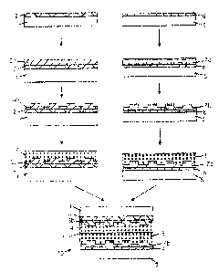
i=;g. I is a schamatic prccsss diagrari for fabrication o` a singie
transparent
phctiovoita'c cefi of ttie present inven':or?.
DesorlaVan c" F'referred Ernb~~r> ii nen's
115 Reterring to F'zC. 1, a process for dasign and fabri(.atioe of a single
transparNnt photovoit;aic celi is ille.istrated.
r ar.aricat~on oi frr.si eJeof; oaYa !errorreJ:
A 3000 i<rri thick firs~ high9y transparent glass substrate 1 is thorougiriy
oic an~ d and drie~i, fr~r axantf,ie by cieaning witf: dist~iled water,
rinsing with
20 acs:tor,:e and dryirsg in air. A 100 prn t;)iclc first PJf1Al grid is
deaasited on tha
su~; tr,-.+.e. by screen :arin:int} to lir=OVitie a firsSt curre"Yt cci;ector
layer 2.
First subatrate I is coated with thin film 3a of a 56-Lei solution of
6nC by spin coatinsr so that first current collector ;ayer 2 is betwaan first
:serostrate
I anct triiri film 3a. Znl.~ ~s a transparent conduotlve oxide. The so?..ge!
solution is
25 ailo,vr:c to dry and thin film 3a is surFa.ce patterned by hot-embossing to
`orrrr
?atters-,ec1 transparent concuctive oxide laver 3b haviny rectangular pattern
c~ernents. Tie patterner transparent conduwtive layer is sintereo. F'attaaned
a
CA 02621665 2008-02-15
::ar;vparent conductive oxtde layer Sb i, 1000 pm thick. The patterri elements
are
0.1 .rm thick and I Wm long, with a separation of 2lim betwe n pattern
eiernents.
A 0.5 prr td?ick n-type sr:rr!`cori:tuctor fi!m 4 is then formed ori patterned
trznsqaren4 cor.ductive oxide layer 3b by spir-Goating. The n-type
semiconductor
c-omprises Guina? nanopariides prepareJ by microwave synthesis as aescribed in
cornr-nonly owned k't;'t' apodi.ation PC,TXA2005lUCJ11 12 filed July ~1, 2006,
the
d;sc:'sosrce of wn8cii is her in incorporated by referenr,a. Solid state
bandgap of
the C;u1n,32 rrancparticfes is about 1,5 elv'. Such Ranoperbcies are soluble
tn water
ar,d easy to disperse,
f o Pabr,f:;aL'oxt cfsecrrnd s!actrcda (catflods.):
A 300r prr thick second higNiy transcarent glass substrate 5 dvith simiiar
ci,mensicns to the first glass substrate is cleaned and dried and coated with
0.3
ihi:ic sillwr d;oxide uarrier layer 6.
A 0.5 pn : thick r;ro(y:acenum fiirr 7a is formed on second giass substrate 5
wa;h barrier layer 6 sandvvyched in betweerc. The molybdenum film is formed by
magnetrur sputtering of a maiyb*Jenurn target. Wlalybd rum fiirn %a is
pattemad
k laser scribing tc iarm patternad metallic flim structure lb having
rectangular
Mrittem elemFrnt.s. Th s pattern caterrants have the same size anG separation
as
rhe pattern P ernant s on the patter7ied TG0 layar.
A 0 2 pm thick p-nyce se!r,iconductor r11m 8 Is then formed on patterned
me,t~.liic film structtare 7h by sw in-coating. The p-type sarniconductor
comprises
C:c Te nanoparticias prepared tfy mrcro,vave synthesis as described in
commor.ly
ownec r+CT apofication PC'lCA2006f001 t 12 fiied July 91, 2006. the disclosure
of
wh& is hrtire9r; incor,pr;ated by reference. Cr;Te is a su4rab!e p4yzin
2: se *~<<~~,rzs9u;.tcr tc fOrm a 3-w i=ietarojunctlnr vrlth GulnB2.
Fa-Pr;cai;car of it-,e phr.fovci!ta(: ae!f.'
The two rrodif~ad y;ast substrates are then laminated together at a
tercpErature of about 150'0 under vacuum to form graded photcvottaic cell 10
having a 34) heterojunctiork 11 at an interface between n-type 4 and p=type B
S
CA 02621665 2008-02-15
semiccntluctor filrivs. At ~E 3-0 heteoJunr.t or),, raat:s oX the n-type and
p-tYpe
semiconduc-or films are noc encfaged in the irtterface. The pattern elernenis
of
tr?.nsl:.arevt canductive ox.ide layer 3b Gnd pa7:erned metaliic fiim
structure 7b are
aliw7ed in the ~..eil.
~ Refarer~cr~s:
Shaheer et Eii ,"2. 5 rb Effinient Orryanic P'astic Solar Gells", AppJted
Physics
Leff6r~, 78:841-843 i20C1 i
Huyrth et ai., "Hybrtd Nancrod-Poiyrner sola: C:lls". Scler?ce,
234(5564;:2.426-
242" flVlarch 29, 24x:2),
Kapur e; al.: "Non-4's,Wuum Pracesslng of CuEn,.%GarSe, Solar Ce61s or. R.ic9d
ard
F{ex;ble Substrates us:n; Nanopart:cle Ini<s" 7ehin Solid Fiirrrs, 431==432
(2003) 53-
i,fS F'z:tent 5,985.691. Basr+l ot al., POetf;cd of IVtslcing Compo!;nd
Semicorid,aL.tor
Fi4me inn POaking Relateck Eiectronlc Geiices", issued hioNeemoer 16.1999.
Kr;ssaier st aiõ :`Progress in Low Cost irlactroceposition of
CG(in,Ga)(S,Se)2: The
CISEL Prcaiect". 20th Europsarr Fhr.fo,vifeic Soldr Eriergy Gont+:arence. 6-10
June
2005, Sarcelona Spain.
US Patent 7,026.256, Taunier ct al., Method for Making 1'hi;'.,.ti::?i
SerTiiconductors
ESasud or I-IIi-Vit Gompou;t¾ts for Photovoltaic ADplioations issuoci Aadl
11,
4,6+)6.
[3isnt e~ e,"CQmpar!son of Spray Pyroierr-~ad F77, ATO ar!d iTeJ Gcetrngs fcr
Flat
and Rer,t C:lass S:rbstrat.es", Tfiin Sof,id Fflrrrs, "j6^ (199G) ? 09- s 14,
Patant 6,34 0,7&ca, f=atritsaf3 et u~aE., "hAultiE,a~~er t~ttotovo!t,ai~: or
Pnotoe~:,nductsve
^vavic.ew`. issuect.january 22, 2002.
?ri US P;:tent 4,611,091, r:huudari at al. "C'u1risSew Tt71n F'ilm Solar Geli
with 1'fiin
udS iar~d Transparent Window t,.aver" isslaec' Septern5gr 9; 19d6. 10
CA 02621665 2008-02-15
Anderson et A!õ "EiectrochTornic ,-iX'rYObi'Poiymer laminate,..", Apgdlesy
CcUcs, 15
US t'atewit 8,481.482, MitsWairo, ,i amirating Apparatus for tvtanufactiiring
Photovoltaic 1<Aodu:e", issi:ed Novernber 19, 2002.
a tJS Patant 6,90.597. Sager et ai., "PhoTovo!taic G+evices Fabrfcs+ted by
Growth
from Pcous Temp"ate", izss en Septernber 20, 200:.
41, Patent 4,663,495, 9erman at ai., 'Transparent Photovottaic MoJuie`, issued
!viay 5. 1987.
Marzolin, et a!., "Fabriraiian of Gias_~~, Wicrostructures= by t.licro-Moltlir
g of SoE-Gal
Precursors'", .4dvancedMarerlafs, 10 (1998) 571-574,
US Patent 7,014.799, Yang et al., Method of Forrn!ng Mesoscop'scatly
Structured
fvqaterial'. issued N,arch 21. 2408.
US patent -3,285,652, Ku ata o al., "Integrated Thin F(!m 5olar Battery ar,G
i\+lethod of RAanufacturing the Sarne", issued July 24. 2001.
15 tJ.8 patant 4,554.727. [}eckmaw et al., "tf9ethod for Fvsaking fJptica!iy
Enhanced
Thin Film Photovcltaic Devic Using l,.Ithograjhy Dei'ined Random Surfaces",
issuec Novcntber 26, 1 95~..
St.iebig, e. :al., `Silicon Tt,ir==tilm Solar t,eiis with Rectang;_,Ãar-shaped
Grating
Cr...zware", Ptvg. Phottavol.= R. Apwtõ C2006? -W13-24.
"wJ Other advanT.ages that are inherent to the structure are obvious to ona
t;l:i!ledi^t the art= 'ftte a,7?bodiments are deEcrit=ed herein illustratvely
and are not
rnc,ait ,o iirnÃt the s.:ope of the invention as ciairnea. Variations of tne
eoracJoiny
arn'e*odirren,+.s will be evident to a person of orc!r!ary s c!!i and are
interd c by the
inventc,r to be enecmpassad by the fcllovving cla+rns.
(?