Note : Les descriptions sont présentées dans la langue officielle dans laquelle elles ont été soumises.
CA 02623453 2008-03-25
WO 2007/047966
PCT/US2006/041109
MRI-SAFE HIGH IMPEDANCE LEAD SYSTEMS
AND RELATED METHODS
Inventors:
Ergin Atalar
Justin Allen
Paul Bottomley
William Edelstein
Parag Karmarkar
Attorney: Julie H. Richardson Attorney Reference No.: 9450-7W0
Myers Bigel Sibley & Sajovec, P.A.
P.O. Box 37428, Raleigh, NC 27627
919-854-1400
CA 02623453 2 0 12 ¨ 11¨ 0 8
Mill-SAFE HIGH IMPEDANCE LEAD SYSTEMS
AND RELATED METHODS
FIRM OF THE INVENTION
[0002] The present invention relates to interventional medical leads and
may
be particularly suitable for MRI compatible implantable devices such as
cardiac pacing
devices and Deep Brain Stimulation ("DBS") and/or sympathetic nerve chain
stimulation
leads.
BACKGROUND OF THE INVENTION
[0003] When patients implanted with deep brain stimulation (DBS) or
cardiac
pacing (CP) lead systems are exposed to external Radio Frequency (RF) fields,
local
tissue damage around the electrodes of these leads can occur as has been
reported by
various researchers. See, e.g., Baker et al., Neurostimulation systems:
assessment of
magnetic field interactions associated with 1.5- and 3-Tesla MR systems, J
Magn Reson
Imaging 2005;21(1):72-77; Bhidayasiri et al., Bilateral neurostimulation
systems used for
deep brain stimulation: in vitro study of MRI-related heating at 1.5 T and
implications
for clinical imaging of the brain; Magn Reson Imaging 2005;23(4):549-555;
Rezai et al.,
Neurostimulators: potential for excessive heating of deep brain stimulation
electrodes
during magnetic resonance imaging. J Magn Reson Imaging 2001;14(4):488-489;
Chou
et al., RF heating of implanted spinal fusion stimulator during magnetic
resonance
imaging, IEEE Trans Biomed Eng 1997;44(5):367-373; and Luechinger et al., In
vivo
heating of pacenzaker leads during magnetic resonance imaging, Eur Heart J
2005;26(4):376-383; discussion 325-377.
[0004] There are several external RF sources such as, for example, RF
2
CA 02623453 2008-03-25
WO 2007/047966
PCT/US2006/041109
exposure during MRI or during RF diathermy. Local tissue damage during RF
diathermy
procedures in patients with implanted deep brain stimulator lead systems has
also been
reported. RF/microwave diathermy treatments can use leads that employ an
alternating
current to cauterize tissue. The diathermy alternating current delivered
during the
therapy can be in the range of between about 1KHz-350 MHz (believed to be
typically at
about 27.5 MHz). In certain situations, the lead system may undesirably act as
an
antenna, receiving and depositing current in localized tissue where the leads
are exposed,
thereby potentially increasing the specific absorption rate (SAR) (a way of
measuring the
quantity of radiofrequency (RF) energy that is absorbed by the body).
[0005] RF heating of tissue in close proximity to long conductors
(such as
metallic wires) in an MRI environment has also been reported in literature.
Local tissue
damage can be caused by RF deposition in the tissue that is in close proximity
to the
linear conductors or electrodes of the lead system, when patients with
implanted leads or
interventional devices are placed in an external RF field. This RF heating
mechanism
may be explained as follows. During an MRI scan, the transmit RF field creates
a
voltage along the long linear conductors (individual or part of any
interventional device)
or the conductors/filers of the DBS and cardiac pacing lead systems. Currents
are then
created through the conductors and into the surrounding tissue. Where the
current
emerges from the distal tip of the device (or adjacent to the electrode in the
case of an
implantable lead), it can be concentrated and can cause heating and subsequent
tissue
damage.
[0006] In view of the foregoing, there remains a need for alternative
medical
lead configurations.
SUMMARY OF EMBODIMENTS OF THE INVENTION
[0007] Some embodiments of the present invention provide therapeutic
lead
systems that can exhibit high impedance during exposure to RF (high
frequencies).
[0008] The lead systems can be used with interventional devices and
may be
acutely placed in vivo or chronically implantable and can include one or more
stimulating, ablating and/or recording electrode. The lead systems may be
particularly
suitable for implantable lead systems for IFIGs (implantable pulse
generators), cardiac
3
CA 02623453 2008-03-25
WO 2007/047966
PCT/US2006/041109
defibrillators, cardiac pacing (CP), neurostimulation (peripheral, deep brain,
or spinal),
EP catheters, guidewires, and the like, for leads used in heat-sensitive
regions in the
body.
[0009] The lead systems may be implantable, MRI compatible multi-
purpose
lead systems with at least one stimulating/pacing electrode and may optionally
be
configured to provide an internal MRI receive antenna.
[0010] In some embodiments, the lead systems can include a plurality
of high
impedance sections or segments spaced along the length of the lead. The high
impedance
sections can be configured as RF traps that inhibit flow of induced RF current
at the high
impedance frequency/frequencies, whereby current is inhibited from heating
tissue
adjacent to one or more electrodes, thus reducing the likelihood of and/or
preventing RF-
current induced tissue damage. The RF traps can be configured to allow
physiological
and stimulation signals to pass through (typically in the kHz range). Thus,
the RF trap
can trap only the high frequencies of interest to which the traps are tuned.
[0011] Embodiments of the invention describe different methods of
creating
high impedance RF traps using the components of an implantable lead system or
a
medical device. The RF traps may be incorporated in long metallic components
to render
them safe to use in an MRI environment.
[0012] The lead systems may include supplemental high impedance
circuits
for the shield in combination with the high impedance configurations for
conductors.
[0013] Some embodiments are directed to interventional devices and/or implant
devices comprising metal or metallic components.
[0014] In particular embodiments, a lead can be a relatively long
implantable
lead having a length in the body of greater than 10 cm. The at least one
electrode can be
a plurality of electrodes with at least one being a recording and/or a
recording and
stimulating and/or ablating electrode.
[0015] Some embodiments are directed to MRI/RF compatible medical
interventional devices. The devices include an implantable elongate lead
system having
at least a first and a second electrode, each associated with a respective
first and second
axially extending conductor. A plurality of axially spaced apart capacitors
are disposed
between the first and second axially extending conductor along at least major
portion of a
4
CA 02623453 2008-03-25
WO 2007/047966
PCT/US2006/041109
length of the lead system to define, a plurality of high impedance circuit
segments
whereby the lead system has a high impedance over a target range of (typically
a high
range) of radiofrequencies and a low impedance over another range of low
electromagnetic frequencies (such as audio-frequencies or frequencies in the
kHz or
lower ranges, including DC at around 0 Hz).
[00161 The high impedance circuit segments may be configured to inhibit
RF
transmission along the lead system during exposure to RF associated with a
high-field
magnet MRI system.
[0017] Other embodiments are directed to MRI compatible device/lead
systems that include: (a) an implantable lead system elongate lead having at
least a first
and a second electrode, each associated with a respective first and second
axially
extending conductor; and (b) a high impedance surface band gap structure
disposed about
the first and second conductors.
[0018] The surface band gap structure may include a primary shield and
secondary and tertiary segmented shields which are intermittently connected to
the
primary shield, whereby the high impedance surface reduces or blocks RF
propagation.
[0019] Other embodiments are directed to an MRI compatible device that
includes: (a) an implantable lead system elongate lead having at least a first
and a second
electrode, each associated with a respective first and second axially
extending conductor,
wherein a plurality of spaced apart capacitors are disposed between the first
and second
axially extending conductors along at least major portion of a length of the
lead system to
define a plurality of high impedance circuit segments; and (b) a high
impedance band gap
surface formed along at least a major length of the lead system. The lead
system has a
high impedance at a high range of radiofi-equencies and a low impedance at a
low range
of frequencies.
[00201 Still other embodiments are directed to MRI compatible
implantable
pulse generators (IPG). The EPG's include: (a) an implantable housing; (b) a
high
impedance decoupling circuit disposed in the housing; (c) at least one
implantable lead in
communication with the decoupling circuit and configured with a length that
extends
from the housing to a target treatment site; (d) at least one implantable
electrode in
communication with the lead; and (e) a controller in the implantable housing,
the
CA 02623453 2008-03-25
WO 2007/047966
PCT/US2006/041109
controller configured to selectively activate the decoupling circuit to
provide a high
impedance to the lead at high radiofrequencies and a low impedance at a low
radiofrequencies.
[0021] In particular embodiments, the controller is remotely
controllable to
activate the decoupling circuit to provide the high impedance.
[0022] The high impedance circuits and/or circuit segments may
comprise
inductors. Inductors and capacitors can be formed form conducting leads and a
dielectric
substrate and can be configured to reduce, block or inhibit RF transmission
along the lead
system during exposure to RF associated with a high-field magnet MRI system,
while
permitting passage of low frequency physiologic signals, treatments and/or
stimuli.
[0023] The lead may be a flexible lead and the at least one electrode
can be a
plurality of spaced apart electrodes. The lead can include a plurality of
conductors held
in a core of the lead, a respective one for each electrode.
[0024] Some embodiments are directed to MRI safe lead systems that
include:
(a) an elongate flexible body with at least one conductor; (b) at least one
electrode in
communication with the at least one conductive lead; and (c) a plurality of
high
impedance segments axially spaced apart along a length of the lead system. The
at least
one conductive lead has a plurality of axially spaced apart coiled segments
and-a plurality
of linear segments residing between adjacent coiled segments. The high
impedance
segments include: (a) a coiled conductive lead segment defining an inductor;
(b) a
dielectric over the coiled conductive lead segment; (c) a conductive shield
over the
dielectric with the dielectric residing between the inductor and the
conductive shield,
wherein the conductive lead is electrically coupled to the shield at a
proximal end portion
of the coiled segment; and (d) a capacitor at a distal end of the coiled
conductive lead
segment electrically connecting the conductive lead and the shield. The high
impedance
segments are configured to provide an impedance that is greater than about 450
Ohms at
a target RF frequency associated with an MRI system.
[0025] Some embodiments are directed to MRI-safe lead systems that
include:
(a) an elongate flexible body with a plurality of conductors, the body having
distal and
proximal portions, the conductors each having a plurality of axially spaced
apart coiled
segments, each coiled segment defining an inductor; (b) at least one electrode
residing at
6
CA 02623453 2014-12-17
55565-47
the distal portion of the flexible body in communication with at least one of
the conductors;
and (c) a plurality of high impedance segments axially spaced apart along a
length of the lead.
The high impedance segments include: (i) a plurality of coiled conductor
segments residing at
a common axially extending segment of the flexible body, at least one coiled
lead segment for
each of the conductors; (ii) a dielectric insulator covering the plurality of
coiled conductor
segments at the common axial segment; and (iii) a conductive shield at the
common axial
segment disposed over the dielectric insulator with the dielectric insulator
residing between
the coiled segments and the conductive shield. A single one of the plurality
of conductors is
electrically coupled to the conductive shield at a proximal end portion of the
common axial
segment.
[0026] Some embodiments are directed to MRI-safe lead systems that include
an elongate flexible body with a plurality of conductors and at least one high
impedance
segment with opposing proximal and distal portions. The at least one high
impedance segment
is configured so that at least one of the conductors has (a) a first
individually coiled segment
that is proximate to but axially apart from the coiled segments of different
leads, and (b) a
second coiled segment that is co-wound with at least one other conductor
coiled segment. A
conductive shield resides over the first lead first and second coiled segments
and an insulating
material resides between the shield and the first and second coiled segments.
The at least one
lead with the individual and co-wound coiled segments is in electrical
communication with
the shield at a proximal portion of the high impedance segment.
[0026a] According to another aspect, there is provided an MRI/RF compatible
medical device, comprising: an implantable elongate lead having at least a
first electrode, a
second electrode, a first axially extending conductor, and a second axially
extending
conductor, the first electrode electrically coupled to the first axially
extending conductor and
the second electrode electrically coupled to the second axially extending
conductor, wherein,
at each of a plurality of intermediate locations along a length of the
elongate lead, at least one
of a plurality of spaced apart capacitors is disposed between the first and
second axially
extending conductors to define a plurality of high impedance circuit segments,
each high
impedance circuit segment comprising at least a portion of the first axially
extending
conductor, at least a portion of the second axially extending conductor, and
at least one of the
7
CA 02623453 2014-12-17
55565-47
plurality of spaced apart capacitors disposed between the portion of the first
axially extending
conductor and the portion of the second axially extending conductor, whereby
the lead has a
high impedance at a target range of high radiofrequencies and a low impedance
at low
frequencies.
10026b] According to a further aspect, there is provided an MRI compatible
device comprising: an elongate lead having at least a first and a second
electrode, each
associated with a respective first and second axially extending conductor,
wherein a plurality
of spaced apart capacitors are disposed between the first and second axially
extending
conductors along at least major portion of a length of the lead to define a
plurality of high
impedance circuit segments; and a high impedance surface band gap structure
formed along at
least a major length of the lead, wherein the surface band gap structure
comprises a primary
shield and secondary and tertiary segmented shields which are intermittently
connected to the
primary shield, whereby the high impedance surface reduces or blocks RF
propagation;
wherein the lead has a high impedance at a high range of radiofrequencies and
a low
impedance at a low range of frequencies.
[0027] Other systems, methods, and/or computer program products according
to embodiments of the invention will be or become apparent to one with skill
in the art upon
review of the following drawings and detailed description. It is intended that
all such
additional systems, methods, and/or computer program products be included
within this
description, be within the scope of the present invention, and be protected by
the
accompanying claims.
BRIEF DESCRIPTION OF THE DRAWINGS
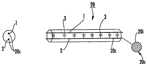
[0028] Figures IA and 1B are schematic illustrations of high impedance lead
systems according to embodiments of the present invention.
7a
CA 02623453 2008-03-25
WO 2007/047966
PCT/US2006/041109
[0029] Figures 2A-2B are schematic illustrations of examples of multi-
electrode lead systems with an IPG, which may include high impedance circuits
or
segments to provide a high impedance operation at selected RF frequencies
according to
embodiments of the present invention.
[0030] Figures 3A and 3C are schematic diagrams that illustrate a lead
system with electrodes and capacitors disposed therealong according to
embodiments of
the present invention. Figure 3A illustrates a linear system and Figure 3C
illustrates a
wound/coiled system.
[0031] Figures 3B and 3D are schematic cross-sectional views of the
systems
shown in Figures 3A and 3B, respectively.
[0032] Figure 4 is a schematic diagram that illustrates three
conductors, three
electrodes and capacitors disposed between conductor pairs according to
embodiments of
the present invention.
[0033] Figures 5A and 5B are schematic diagrams of other multi-
electrode
high impedance leads according to embodiments of the present invention.
[0034] Figure 6 is a schematic illustration of an implantable pulse
generator
with a high impedance operation according to embodiments of the present
invention.
[0035] Figures 7 and 8 are data charts/graphs of a coiled parallel
inductor pair
in a frequency range of between 1-150MHz.
[0036] Figures 9 and 10 are data charts/graphs of a coiled parallel
inductor
similar to that shown with respect to Figures 7 and 8, but modified with
capacitors to
provide higher impedance according to embodiments of the present invention.
[0037] Figure 11 is a schematic illustration of the parallel inductors
and
capacitors used to provide the data of Figures 9 and 10 according to
embodiments of the
present invention.
[0038] Figure 12 is a graph of a sample loss of an open circuit for a
frequency
range of about 1- 150 MHz.
[0039] Figure 13A is a schematic illustration of an electrode lead
system with
a high-impedance surface shield according to other embodiments of the present
invention.
8
CA 0 2 62 3 4 53 2 0 12 ¨ 11¨ 0 8
[0040] Figure 13B is a section view of the lead system shown in Figure
13A
illustrating shielding and conductor configurations according to embodiments
of the
present invention.
[0041] Figure 13C is a cross-sectional view of the lead system shown in
Figure 13B.
[0042] Figure 14 is a schematic illustration of a lead system with RF
chokes
that may be combined with one or more of the high impedance configurations
shown
and/or described herein according to embodiments of the present invention.
[0043] Figure 15A is a schematic illustration of an RF trap that can be
used to
form a high impedance segment on a lead according to embodiments of the
invention.
[0044] Figure 15B is a schematic illustration of the RF trap shown'in
Figure
15A with the addition of a capacitor connecting the shield and the conductor
according to
some embodiments of the invention.
[0046] Figure 16 is a schematic illustration of a long lead with a
plurality of
axially spaced apart RF traps along a length of a conductor or lead according
to
embodiments of the invention. =
[0047] Figure 17 is a schematic illustration of a lead system with RF
traps
having co-wound conductors in a common shield according to embodiments of the
invention.
[0048] Figure 18A is a partial cutaway side view of a multi-lead system
with
an RF trap having co-wound conductors/filars according to some embodiments of
the
invention.
[0049] Figure 18B is a cross-section view taken along lines 18B-18B in
Figure 18A.
[0050] Figure 18C is a schematic line illustration of the embodiment
shown
in Figure 18A.
[0051] Figure 19A is a partial cutaway side view of a multi-lead system
with
an RF trap having co-wound conductors/filars with capacitors connecting the
respective
9
CA 02623453 2008-03-25
WO 2007/047966
PCT/US2006/041109
leads to the conductive shield at two locations according to some embodiments
of the
invention.
[0052] Figure 19B is a cross-section view taken along lines 19B-19B in
Figure 19A.
[0053] Figure 19C is a schematic line illustration of the embodiment
shown
in Figure 19A.
[00541 Figure 20A is a partial cutaway side view of a multi-lead
system with
an RF trap having co-wound conductors/filars with less than all the
leads/conductors in
electrical contact with the shield according to some embodiments of the
invention.
[0055] Figure 20B is a cross-section view taken along lines 20B-20B in
Figure 20A.
[0056] Figure 21A is a partial cutaway side view of a system with an
RF trap
having conductors coiled both separately and co-wound according to some
embodiments
of the invention.
[0057] Figure 21B is a cross-section view taken along lines 21B-21B in
Figure 21A.
[00581 Figure 21C is a schematic line illustration of the embodiment
shown
in Figure 21A.
[0059] Figure 22 is a graph of impedance (Ohms) versus frequency (MHz)
for the embodiment shown in Figures 21A and 21B.
DETAILED DESCRIPTION OF EMBODIMENTS OF THE INVENTION
[0060] The present invention will now be described more fully
hereinafter
with reference to the accompanying drawings, in which embodiments of the
invention are
shown. This invention may, however, be embodied in many different forms and
should
not be construed as limited to the embodiments set forth herein; rather, these
embodiments are provided so that this disclosure will be thorough and
complete, and will
fully convey the scope of the invention to those skilled in the art. It will
be appreciated
that although discussed with respect to a certain embodiment, features or
operation of one
lead system embodiment can apply to others.
CA 02623453 2008-03-25
WO 2007/047966
PCT/US2006/041109
[0061] In the drawings, the thickness of lines, layers, features,
components
and/or regions may be exaggerated for clarity and broken lines illustrate
optional features
or operations, unless specified otherwise. In addition, the sequence of
operations (or
steps) is not limited to the order presented in the claims unless specifically
indicated
otherwise. It will be understood that when a feature, such as a layer, region
or substrate,
is referred to as being "on" another feature or element, it can be directly on
the other
element or intervening elements may also be present. In contrast, when an
element is
referred to as being "directly on" another feature or element, there are no
intervening
elements present. It will also be understood that, when a feature or element
is referred to
as being "connected" or "coupled" to another feature or element, it can be
directly
connected to the other element or intervening elements may be present. In
contrast, when
a feature or element is referred to as being "directly connected" or "directly
coupled" to
another element, there are no intervening elements present. Although described
or shown
with respect to one embodiment, the features so described or shown can apply
to other
embodiments.
[0062] Unless otherwise defined, all terms (including technical and
scientific
terms) used herein have the same meaning as commonly understood by one of
ordinary
skill in the art to which this invention belongs. It will be further
understood that terms,
such as those defined in commonly used dictionaries, should be interpreted as
having a
meaning that is consistent with their meaning in the context of the relevant
art and this
specification and should not be interpreted in an idealized or overly formal
sense unless
expressly so defined herein.
[0063] The term "high radiofrequency" or "high RF" refers to RF
frequencies
that are at or above about 1 MHz, and includes radiofrequencies in the range
of about
1MHz to about 256 MHz. Embodiments of the present invention configure devices
so as
to have high impedance circuit segments or a high impedance circuit at high RF
and low
impedance circuit segments or circuit at DC or low frequency (at a kHz or less
frequency
or frequency range), i.e., at frequencies used for treatment such as
stimulation or ablation.
For example, for 1.5T, 3.0T and 6.0T systems, the respective frequencies are
64 MHz,
128 MHz and 256 MHz. The frequencies of the different MRI systems are well
known to
those of skill in the art. The devices can be configured to have high
impedance at several
11
CA 02623453 2008-03-25
WO 2007/047966
PCT/US2006/041109
of the yadiofrequencies associated with high-field magnet MRI systems, such as
systems
with magnets above about 1.0T, such as about 1.0T, I.5T, 2.0T, 3.0T, 4.0T,
5.0T, 6. OT
and 9.0T, typically between about 1T to 15T.
[00641 The term "high impedance" means an impedance sufficiently high
to
inhibit, block or eliminate flow of RF-induced current at a target frequency
range(s). The
impedance has an associated resistance and reactance as is well known to those
of skill in
the art. Some embodiments provide an impedance of at least about 300 Ohms,
typically
between about 400 Ohms to about 600 Ohms, such as between about 450 Ohms to
about
500 Ohms, while other embodiments provide an impedance of between about 500
Ohms
to about 1000 Ohms. Embodiments of the invention configure lead systems that
provide
sufficiently high-impedance at frequencies associated with a plurality of
different
conventional and future magnetic field strengths of MRI systems, such as at
least two of
1.5T, 2.0T, 2.5T, 3.0T, 9.0T, and the like, allow for safe use in those
environments
(future and reverse standard MRI system compatibility).
[0065] The term "tuned" means that a parallel resonant circuit with
inductive
and capacitive characteristics defined by certain components and
configurations has a
high impedance at one or more target frequencies, typically including one or
more MRI
operating frequencies.
[0066] The term "coiled segment" refers to a conductive lead (trace,
wire or
filar) that has a coiled configuration. The term "co-wound segments" means
that the
affected leads, conductors, wires and/or filars can be substantially
concentrically coiled at
different radii, one above the other, or concentrically coiled closely spaced
at
substantially the same diameter. The term "co-wound" is used to describe
structure and
is not limiting to how the structure is formed (i.e., the coiled segments are
not required to
be wound concurrently or together, but may be so formed). The terms
"conductive
element", "conductive lead" and "conductors" are used interchangeably and
refer to a
conductive path that connects target components (such as, for example, a
stimulation
source and an electrode) and can include one or combinations of a metallic
trace, a wire,
a flex circuit, a filar(s), or other conductive configuration. As such, the
conductors or
conductive elements include long linear and/or non-linear conductors that can
be formed
with one or more of discrete wires, flex circuits, filars (bi, quadra or other
winding), or by
12
CA 0 2 6 2 3 4 5 3 2 0 12 ¨ 11 ¨ 0 8
plating, etching, deposition, or other fabrication methods for forming
conductive
electrical paths.
[0067] Embodiments of the present invention can be configured to for any
desired internal region of the body or object. The object can be any object,
and may be
particularly suitable for animal and/or human subjects. Some embodiments can
be sized
and configured for brain stimulation, typically deep brain stimulation. Some
embodiments can be configured to stimulate a desired region of the sympathetic
nerve
chain and/or the spinal cord. Some lead or implantable devices can be
configured for
cardiac intervention. Other embodiments may be directed to other anatomical
structures,
organs or features including deep tissue, lumens, and the like. For example,
the systems
of the present invention may be configured for treatment of gastrointestinal,
urinary, or
other body regions. Some embodiments provide devices configured for
intraluminal Or
intratissue penetration. Some embodiments provide devices for acute or chronic
implantation.
[0068] Examples of known stimulation treatments and/or target body
regions
are described in U.S. Patent Nos. 6,708,064; 6,438,423; 6,356,786; 6,526,318;
6,405,079;
6,167,311; 6539,263; 6,609,030 and 6,050,992.
[00691 Generally stated, the extent to which the lead system or the long
conductor couples with the external RF is a function of length of the lead
system or the
conductor, the insulation thickness over it and its arrangement in the RE
field e.g. looping,
etc. Typically, lengths shorter than quarter wavelength (at the applied RE
frequency) do
not couple with the external RE fields, displaying reduced RE deposition and
lower local
temperature rise in tissue adjacent to them. Also, typically, increasing the
insulation
thickness can reduce the coupling and RE deposition in the adjacent tissue.
[0070] Long wires, conductors and lead systems couple to external RF to
different extents at different frequencies. The extent of RE deposition in the
tissue
depends on the extent of resonation, i.e., the coupling at that frequency.
Linear
conductors/wires act as linear antennas. Lead systems which have more than one
long
conductor act as linear antennas, where each individual conductor acts as an
antenna and
two or more conductors in combination with each other act as antennas too.
This creates
13
CA 0 2 62 3 4 53 2 012 ¨11¨ 0 8
a RF coupling pattern having the lead system couple at multiple/different
frequencies.
DBS and cardiac pacing leads may comprise about 8 (and may include more pr
less) long
conductors and electrodes. In particular embodiments, one, some or all of the
conductors
can act as antennas individually and in combination with each other.
[0071] Internal and external imaging coils used in MR1 can be decoupled
during RF transmit by the scanner. This can inhibit local heat deposition in
the tissue
adjacent to the coils. The decoupling mechanism can create a high impedance
circuit so
that these coils do not couple with the transmitted RF, thus eliminating any
tissue damage.
See, Yoda K., Decoupling technique for transmit coils in NMR spectroscopy and
imaging,. NMR Biomed 1990;3(1):27-30; and Buchli et al., Increased RF power
absorption in MR imaging due to RF coupling between body coil and surface
coil, Magn
Reson Med 1989; 9(1):105-112.
100721 Similarly, standing wave formation on long coaxial cables may be
attenuated by incorporating balun circuits or RF chokes at various locations
on the shield
of coaxial cables. See, Atalar et al., U.S. Patent No. 6,284,971, entitled,
Enhanced Safety
Coaxial Cables. See also, Ladd et al., Reduction of resonant RF heating in
intretvascular catheters
using coaxial chokes, Magn Reson Med 2000; 43(4): 615-619. See also, PCT
Application
Serial No., PCT/US2005/028116, filed August 9, 2005, entitled, Implantable MRI
Compatible Stimulation Leads and Antennas and Related Systems and Methods.
Generally
stated, this application describes incorporating RF chokes on DBS and C:P lead
systems.
[0073] Shielding linear conductors can inhibit RF deposition on them.
This
shielding can be continuous, discontinuous, or may be achieved by multiple
methods, to
list a few, e.g., insulating conductors with polymers filled with conducting
metals doped
for conductivity.
[0074] Referring now to the figures, in some embodiments as shown in
Figures 1A and 1B, a high impedance lead assembly 20 can employ at least one
conductor 20c, shown as two conductors 1,2 which may be coiled (Figure 1B)
and/or
reside parallel (Figure 1A) to each other, or be configured with combinations
of both,
14
CA 0 2 62 3 4 53 2 0 12 ¨ 11 ¨ 0 8
and that are operational over a relatively wide range of frequencies. These
long
conductors 20c can have a metal core and are typically insulated from each
other along
their length and may be surrounded by a polymeric dielectric 20i. At
intermediate
locations, the two conductors 1,2 can be connected by capacitors 3. The
combination of
the length of the conductors 1 and 2 (which can also form inductors) and the
capacitors 3
can be configured to create a high impedance circuit(s). This circuit can be
configured so
that it does not tune to a target range of RF frequencies, including for
example,
frequencies ranging from about 1 MHz to 250 MHz, creating high impedance
circuit
segments, thus reducing the extent of coupling in this frequency range. In
operation, the
circuit has high impedance to high RF, but has low resistance to DC, or low
frequency
RF (KHz), which is the stimulation frequency. This principle may be applied to
designing RF/MRI-safe devices and/or lead systems for CP leads, DBS leads,
spinal cord
stimulation leads, etc.
[0075] The capacitors 3 can be regularly spaced or irregularly spaced.
The
capacitors 3 may have the same or different capacitance from each other.
[0076] Lead systems 20 can comprise a plurality of electrodes and
conductors,
such as between about 2 to about 10 conductors, typically at least about 4. In
some
embodiments, the lead systems can include about 8 conductors. The conductor
axial
lengths (linear and/or coiled) can range from about 10 to 200 cm, with a thin
insulator
layer on the conductors and with a polymeric dielectric insulator layer over
it.
[0077] Design of conventional known lead systems with multiple
electrodes
1001-1004 and conductors 20c are shown in Figures 2A-2B. See also, U.S. Patent
Application Publication No. 2005/0222647.
[0078] Referring to Figures 3A and 3B, at a distal end portion of the
lead
system 20, the conductors 20c can be connected to electrodes 1001, 1002,
which, in
position, can be in contact with target tissue. The conductors 20c run along
the length of
the lead system and are terminated by connecting to electrodes 1001 and 1002
at the distal
end. At the proximal end these conductors are connected to the pulse generator
(IPG).
The conductors are typically made of stainless steel or other conducting non-
ferromagnetic material. The concepts described herein can be implemented in
creating a
CA 02623453 2008-03-25
WO 2007/047966
PCT/US2006/041109
high impedance lead system for multi-electrode leads such as those shown in
Figures
2A-2E.
[0079] In some embodiments, as shown in Figures 3A, two
(straight/linear)
parallel conductors 8 and 9 are connected to each Other at intermediate
locations by
capacitors 10 along the length of the lead system to form high impedance
sections. The
capacitors 10 can be semiconductor-based discrete products or can be otherwise
provided,
such as using coatings of metal oxides, e.g. tantalum oxide, and the like at
discrete certain
locations so as to connect the two conductors 8, 9 at desired locations.
[0080] Figure 3B, similar to Figure 3A, illustrates two parallel
conductors
but as wound conductors 1, 2 with spaced capacitors 3 in communication
therewith and
two respective electrodes 1001, 1002.
[0081] In embodiments that employ more than two conductors 20c, more
than
one high impedance circuit can be formed with different conductor pairs. For
example,
as shown in Figure 4, where there are three electrodes 1001, 1002, 1003 and
three
conductors 20c, labeled as elements, 8, 9, and 12, respective capacitors 10
can be
disposed between conductor pairs (8, 12 or 12, 9, as shown). Also, one
conductor 20c
may be used in combination with two conductors to form two separate high
impedance
circuits.
[0082] In some embodiments, the lead systems 20 can conduct DC or a low
frequency AC (KHz), typical of stimulation current. The conductors 20c may be
made
of any suitable (MR1 compatible and/or non-ferromagnetic) conducting material
and/or
metal, e.g., Nitinol, Cobalt-Chromium alloy, MP35N alloy, gold, silver,
platinum,
platinum-iridium alloy, stainless steel, copper and other non-ferromagnetic
materials,
which will not cause a susceptibility artifact in MRI or magnetically react to
the magnetic
field in an MRI scanner environment. DC conductivity is a bulk phenomenon and
RF
conductivity is a skin depth phenomenon. The RF conductivity of the lead
system may
be reduced by using composite wire (a conductor or wire formed of a
combination of
different conductive materials) such as by using a resistive metal such as
tungsten,
MP35N or Nitinol wire on the outside and with a conductive core formed of
gold, silver
or copper or other metals. This may reduce RF transmission along the length of
the lead
system, thus reducing the amount of RF that may be deposited in the tissue.
Further,
16
CA 02623453 2008-03-25
WO 2007/047966
PCT/US2006/041109
these leads made of composite wires (with a resistive outer layer and
conductive core)
can have an insulator coating on the outer surface and may be connected by
capacitors to
form high impedance RF circuits along the length of the lead system as
described above
with respect to Figures 1-4.
[0083] Figures 5A and 5B illustrate lead systems formed with high
impedance segments of two or more insulated conductors 20c with any single
conductor
and/or a composite conductor structure having a polymeric layer 13 over them.
As
shown, the leads may be further shielded by a polymeric dielectric material
with metal or
conductive particulates 13c (Figure 5A) dispersed therein to shield/deflect
external RF.
In some embodiments, the polymeric dielectric or insulation 13c over the
conductors 20e
may be filled/dispersed or mixed with another high dielectric constant
material, e.g.,
titanium dioxide, etc., to regulate the impedance between two or more)
conductors.
[0084] Also, or alternatively, conductive shielding 325 as a continuous
or
discontinuous conductor layer (braided, coated, etc) may be applied over the
conductors
20c of the lead system as shown in Figure 5B. An insulating polymeric material
13 may
reside between the conductors 20c1, 20c2 and the shield 325. A polymer outer
layer 21
may encase the lead system 20.
[0085] In some embodiments, as shown in Figure 14, RF chokes 64rf, as
described in PCT Application Serial No., PCT/US2005/028116, filed August 9,
2005,
entitled, Implantable MRI Compatible Stimulation Leads and Antennas and
Related
Systems and Methods, may be incorporated over these high impedance segments or
leads
to further prevent formation of standing RF waves.
[0086] In some embodiments, as shown in Figure 6, an IPG 102 can have a
lead system 20 with multiple conductors 20c that connect distal electrodes
100. The IPG
may optionally include a decoupling circuit 200 which can be incorporated in
an
implanted housing of the LPG 102 and/or in a connector or portion of the IPG
lead
assembly (a connector or end portion of the lead assembly rather than the
housing itself).
The IPG 102 can include a power source 102b, such as a battery. The circuit
200 can be
in communication with a digital controller 121 that can programmatically
activate the
circuit 200 (and/or deactivate the circuit 200). The lead system 20 may
optionally be
arranged as an antenna described earlier with two or more capacitor sets per
antenna.
17
CA 02623453 2008-03-25
WO 2007/047966
PCT/US2006/041109
[0087] Implantable IPGs can be used with other lead system
configurations
(see, e.g., Figures 15-22). The lead system can be transformed to a high
impedance lead
(and/or antenna) by activating the decoupling circuit 200 to a short circuit,
before an MRI
scan or exposure to external RF. This activation can create a high impedance
circuit with
the capacitors and inductor assembly in the lead body making the lead
electrically
invisible to the external RF thus reducing coupling with the RF. The
decoupling may
comprise a single or multiple circuits tuned to different frequencies and can
be
programmed to be activated accordingly. The activation and/or adjustment to
different
RF frequency and/or deactivation can be carried out by a wireless command sent
to the
IPG. The activation may be carried out internally (automatically) in response
to detection
of an RF signal.
[0088] Some lead systems 20 of the instant invention can be configured
so that
one or more conductors behave as inductors or comprise inductive components.
The
inductors can be provided by coiled conductor (wire) segments, flexible
dielectric
substrates, or other inductor configurations. In some embodiments, at high
frequency,
capacitors can act as shorts and may not, by themselves, give sufficiently
high impedance.
Thus, the lead systems 20 can include inductors that cooperate with the
capacitors. The
leads or conductors of the systems can have high impedance at high frequency
and low
impedance at low frequency by configuring the conductors (wires/leads) to
behave as
inductors.
[0089] In some embodiments, at least one conductor 20c of the lead
system 20
comprises a wound coil segment of the at least one conductor to define a coil
inductor. In
particular embodiments, the coil inductor may be wound to encase other another
conductor(s) of the lead system. The coil inductor can be formed as
substantially an
entire length of a first conductor or as a smaller portion of the conductor.
The capacitors
can connect sections of the coil inductor and a second conductor.
[0090] Figures 7 and 8 are graphs of data associated with a 12 cm long
coiled
inductor pair open at both ends when loaded in saline. The conductors are 32
AWG
magnet wire closely wound on a 0.020 inch mandrel. The graph shows an X-axis
frequency sweep from 1.0 to 150 MHz. The two-conductor assembly tunes at
different
frequencies to different extents as represented by the arrows in Figure 8.
= 18
CA 02623453 2008-03-25
WO 2007/047966 PCT/US2006/041109
[0091] Figures 9 and 10 illustrate the same parallel inductors as
described
above (Figures 7 and 8) with 0.5 pF capacitors placed at about 2.5 cm apart at
5 locations.
The return loss is flatter and higher than -8 db for all frequencies. It is
contemplated that
this loss can be further reduced (closer to zero) in an optimized design.
[0092] Figure 11 is a schematic diagram of the parallel inductors with
the
inductor coil 1 being the wider outside strip and the inductor coil 2 being
the inner strip
(slightly thinner). The 0.5 pF inductors (3, 4) are shown positioned between
the two
inductors 1, 2 to create a high impedance system at the frequency range or
ranges of
interest.
[0093] Figure 12 is a graph of a sample return loss of an open circuit
for a
frequency range of between about 1-150MHz.
[0094] Figure 13A illustrates another embodiment of an MRI/RF safe
lead
system with an IPG connector 22 and IPG electrical connections 23. As shown,
the lead
system 20 includes a plurality of electrodes 100, respective conductors/wires
20c, a
primary shielding 33, a segmented secondary shielding 34, segments /inductors
35, and a
segmented tertiary shield 36. The segments/inductors 5 connect the secondary
34 and
tertiary shield 36 to the primary shield 33. The lead system 20 and/or the
conductors 20c
of the lead system are shielded by one or more layers of shield arrangements
as shown in
Figure 13A. This creates a high impedance surface and inhibits RF coupling of
the lead
system and any formation and/or transmission of a standing wave. This may be
defined
=
as a "3-D RF band gap structure" 39 which is an RF open circuit, while being a
DC
(and/or potentially a low frequency AC) short circuit. This structure can
include a thin,
typically two-dimensional, pattern of capacitive and inductive elements, which
act as
miniature parallel resonant circuits which block RF propagation.
[0095] In some embodiments, the conductors 20c can be coiled
individually or
co-wound, or combinations of each. At one end portion, typically a proximal
end portion
of the segment, the conductors 20c can be selectively connected to the high
impedance
shield directly or indirectly in a capacitor which act as an RF open and low
frequency
(DC) open circuit.
[0096] Figure 13B illustrates an exemplary axial sectional view of the
device
shown in Figure 13A. Figure 13C is a cross-sectional view. As shown, a polymer
19
CA 02623453 2008-03-25
WO 2007/047966
PCT/US2006/041109
dielectric insulating overcoating 21 can be applied to the lead system 20. As
also shown,
dielectric/insulation layers 46, 48, 40 may be disposed intermediate the
shielding layers
33 (primary shield), 34 (segmented secondary shield), and 36 (segmented
tertiary shield).
The conductors 20c extend to connector 22 and electrical connections 23 to the
IPG or
other stimulation, ablation or recording device. Capacitors 24 (Figure 13A)
are not
required according to some embodiments of the present invention, as the
segmented
shielding configurations and inductor lead configuration may provide suitable
impedance
at high frequency.
[0097] Figure 14 illustrates an electrode arrangement with RF chokes
64rf
that can be used with high impedance circuits/segments and configurations
described
and/or shown herein. Each electrode 100 is typically in communication with at
least one
of the insulated conductors 20c. At the proximal end of the lead support body
20, the
conductors 20c are connected to a connector 22 with electrical connections 23
so as to be
connected to the implantable signal generator 102 or to an external circuit,
such as an
interface circuit 40 during MR1 guided lead/cable placement. The lead support
body 20
need not be able to provide MRI signals (i.e. , it can optionally be
configured with an MRI
receive antenna). These insulated conductors 20c are typically covered with a
polymeric
insulator sleeve 61 and a conducting material is cylindrically layered to form
the first
shielding layer 62 over the insulator. This shielding 62 may be terminated
proximal to
the electrodes 100 and, in this embodiment, may not be in electrical contact
with the
conductors and/or the electrodes. A second insulator/polymeric/dielectric
layer 63 further
insulates this shielding 62 to form multi-core coaxial type cable system, with
an
impedance that is typically between about 10-100 ohms. The RF chokes 64rf can
be
integrated or built into the shielding 64 in the form of a second shielding,
which is not
continuous and has multiple sections each X/4 or less in length. As shown in
Figure 14,
at the proximal end, each section or segment 64s is connected to the primary
shielding
62, and the distal end may not be electrically connected to the primary
shielding 62, or is
connected with a capacitance 164 in between the primary and secondary
shielding 62, 64,
respectively. A top insulator/polymeric layer 65 can be used to insulate the
body 20b,
except for the electrodes 25.
CA 02 62 3453 2 0 12 ¨ 11¨ 0 8
[0098] As shown by the axial arrow in Figure 14, the MRI active portion
of
the antenna 35 may extend between a location where the primary shield 62
terminates
and the first electrode 251. However, other antenna 35 configurations may also
be used.
As shown, the second shield layer 64 comprises a plurality of axially spaced
apart RF
chokes 64rf. The term "RF chokes" refers to a shielding layer configuration
that
provides an electrical length of less than or equal to X/4 (from the
perspective of external
electromagnetic waves) to inhibit the formation and/or propagation of RF
induced current
or standing waves in an AC (alternating current, e.g., diathermy applications)
or RF
exposure environment. The physical length that provides the electrical
wavelength may
vary depending on the materials used in fabricating the catheter or lead
system support
body (such as dielectric constant) and the magnetic field in which it is used.
In some
embodiments, the lead system 20 has a physical length that is greater than 10
cm,
typically between about 20 cm to about 150 cm. In some embodiments, the
implantable
lead segment 50 can also include RF chokes 64rf formed along target regions or
along
substantially the entire implantable length. In the embodiment shown in Figure
14, the
RF chokes 64rf comprise a plurality of disconnects of the shield 64 and/or
discrete
electrically isolated second shield segments. In other embodiments, the RF
chokes 64rf
can include a series of axially spaced apart Bahm circuits or other suitable
circuit
configurations. See, e.g., U.S. Patent No. 6,284,971, for additional
description of RF
inhibiting coaxial cable that can inhibit RF induced current.
[0099] As shown in Figure 14, the second shield layer 64 may be coupled
to
the first shielding layer 62 at opposing ends of the segments 64s. As shown,
one end
(typically the proximal end portion) of the disconnected segment 64s is
directly coupled
to the shielding layer 62 and the other end (typically the distal end portion)
is capacitively
coupled to the first shielding layer 62. Each segment 648 may be configured to
engage
the first shield layer 62 in the same manner or in an opposing different
electrical manner
(not shown).
[0100] Figures 15A-15B illustrate lead systems 20 with at least one high
impedance segment 300 with associated axially spaced apart proximal and distal
portions,
300p, 300d, respectively. The high impedance segment 300 can be described as
an RF
21
CA 02623453 2008-03-25
WO 2007/047966
PCT/US2006/041109
trap that includes a conductor 20c being coiled to define an inductor 310
within a
conductive shield 325 and with an insulator/dielectric material 330 between
the inductor
310 and shield 325. The conductor 20c can be in electrical communication with
the
conductive shield 325 at one end (shown in Figure 15A as the proximal end
portion
300p) of the high impedance segment 300.
[0101] The implantable lead system can include multiple high impedance
sections or segments 300 along the length of the lead. The high impedance
sections or
segments are created by arranging the components of the medical device, i.e.,
the
conductor, etc. as an RF trap. These high impedance RF traps inhibit the flow
of induced
RF current (at the frequency to which the RF trap is tuned) and prevent it
from heating
tissue adjacent to the electrodes, thus minimizing or preventing RF induced
tissue
damage. Since the physiological and stimulation signals are at low frequencies
(KHz
range), the RF trap allows the lower frequency signal(s) to go through,
trapping only the
higher frequencies of interest to which the traps are tuned.
[0102] As shown in Figure 15A, the conductor 20c can be in electrical
communication with the shield at the distal portion of the high impedance
segment 300
via a tuning capacitor 340. The high impedance segment 300 (e.g., RF trap) can
be tuned
to a MRI frequency. The segment 300 can also be configured so that the
conductor 20c
at the proximal end portion of the segment 300p is connected to the shield 325
via a
capacitor 360. Different high impedance segments 300 may be tuned to different
MRI
frequencies (i.e., 64 MHz and 128 MHz or other standard operating frequencies
of
commercial MRI scanners). The impedance of the segment 300 can be at least 400
Ohms, typically greater than about 450 Ohms. The at least one high impedance
segment
300 can be placed at between about 0.1-12 cm from the electrode(s) 100. The
lead 20c
can be configured with a straight segment 311 that merges into the coiled
segment 310.
[0103] In operation, the RE' trap 300 with the shield 325, inductor
310 and
tuning capacitor 340 form a high impedance parallel resonant circuit at the
desired
frequency to block RF currents along the conductor. The tuning capacitor can
include
one or more of a discrete capacitor 340 (Figure 15A) and/or stray capacitance
350
(Figure 15B) between the inductor 310 and the shield 325.
[0104] Figure 15B illustrates that the high impedance segment 300 may
22
CA 02623453 2008-03-25
WO 2007/047966
PCT/US2006/041109
include stray capacitance 350 that resides between the conductive shield 325
and the
inductor 310 through the insulator/dielectric 330. The stray capacitance 350
and/or the
discrete capacitor 340 can be used to tune the RF trap to a high-impedance at
a desired
frequency (range), typically between 1MHz to 250MHz. Another capacitor 360 may
also
be used at the opposing end of the segment 300 to form an RF short (not
shown). The
high impedance segment 300 can be tuned to achieve high impedance at desired
frequencies by varying the length of the trap structure, thereby increasing or
decreasing
the total capacitance and inductance until the resonant condition is met at
the desired
frequency. Different segments 300 along a lead length 20 can be tuned to a
different
(typically MHz) frequency.
[0105] As shown in Figure 16, a conductive lead 20c can include a
plurality
of high impedance segments 300 that can be positioned along the length of the
lead
system 20 at regular or irregular intervals, but typically so that the spacing
provides an
electrical length of less than about 7/4 therebetween. The RF traps 300 are
placed less
X/4 apart, where 2,, is the wavelength in the medium of the operating
frequency, to
electrically break the long conductor into multiple sections.
[0106] Figure 17 illustrates that a plurality of conductors 20c1, 20c2,
20c3 can
be co-wound (see element 310c) and reside within a common flexible shield 325.
Each
conductor 20c1, 20c2, 20c3 can be electrically connected to the shield 325 at
a proximal
portion thereof, directly or indirectly, such as using a respective capacitor
360 as shown.
The capacitor 360 can provide an RF short. The high impedance segments 300 (RF
traps)
are placed less than a X/4 apart from each other at the desired frequency.
[0107] When multiple high impedance segments 300 (using, for example RF
traps) are incorporated over the length of a device such that the distance
between two
adjacent traps is less than one-quarter wavelength, this effectively breaks
the long
conductor into multiple sections, each shorter than a quarter wavelength. The
RF current
induced on a conductor is a function of length of the conductor at the RF
frequency, and
when the conductor is shorter than a quarter wavelength, the RF current
induced is not
large enough and may not cause undue RF deposition RIP induced-treating of the
tissue.
[0108] For a bare copper wire X/4 in a physiological medium, the length
has
been measured at about ¨ 8 cm at 64 MHz (1.5T) and 4 cm at 128 MHz (3T). For
23
CA 02623453 2008-03-25
WO 2007/047966
PCT/US2006/041109
implantable leads where the conductors are insulated with a polymeric layer of
about or >
0.001 inches thick, and have an electrode exposed to tissue, the temperature
change in the
tissue adjacent to the electrode due to RF deposition is measured to be less
than 1 C at
length less than 15 cm at 1.5T (64 MHz frequency). When a high impedance
segment or
section 300 (using one or more RF traps) is incorporated in the length of the
conductor
20e, the section 300 can be positioned such that the distal end of the trap
300d is less than
15 cm from one or more of the electrodes 100 and the impedance can be greater
than
about 450 Ohms at a target MRI frequency, in order to reduce RF deposition
induced
heating at the electrodes (less than 1 C). Thus, in some embodiments, multiple
segments
300 with impedance of about or greater than 450 Ohms (at 64 MHz) are placed at
distances less than 15 cm apart on a long conductor, which can make the
conductor 20e
safe to use in MRI at 1.5T. Similarly if these segments 300 have an impedance
of about
or greater than 450 Ohms at 128 MHz and are placed <10 cm apart (Length ¨ k/4
at 128
MHz, or 3T MRI frequency), it can effectively reduce the extent of heating at
the
electrode in a 3T MRI environment.
[0109] Different designs of high impedance segments 300 along the
length of
the leads for multi-conductor lead systems with electrodes are described
herein. Such
high impedance segments 300 can be placed along the length (less than 2/4
length apart
from each other) of the lead 20 to reduce RF deposition at the electrodes 100
and inhibit
undue tissue damage.
[0110] Figures 18A-18C illustrate a high impedance segment 300 with
four
co-wound conductors/filars 20c1-20c4 and a shield 325 placed over the co-wound
conductors 310e which is connected to the conductors 20c1-20c4 at the proximal
end of
the trap 300p via respective capacitors 360. The capacitor 360 can have a
relatively large
capacitance sufficient to act as an RF short and a DC and low frequency (Hz,
kHz) open
circuit. The connection 370 can be via a metallic trace, small wire or other
connection
from a linear segment 311 of the conductor 20c to the shield 325 as the
conductor 20c
merges into a coiled segment 310. A polymeric outer layer 21 can be provided
over the
shield 325. The lead system 20 can be a flexible lead system and the
dielectric material
330 can be provided as a flexible material.
[0111] As shown in Figures 18A and 18B, for a lead 20 comprising one or
24
CA 02623453 2008-03-25
WO 2007/047966
PCT/US2006/041109
more insulated filars/conductors 20c, the filars/conductors 20c can have a
straight section
311 followed by a coiled section 310 that forms the inductor. The coiled
section 310 may
be co-wound with another filar/conductor. A dielectric/insulator 330 can be
placed on the
coiled section 310 and a shield 325 can be placed on the co-wound conductors
separated
by the dielectric 330 between them. As shown, at the proximal end portion of
the coil
310, the shield 325 is connected (via trace or wire 370) to each conductor
20c1-20c4 by a
capacitor 360 which acts as an RF short at high frequencies and a DC and low
frequency
open circuit.
[0112] Although the tuning capacitor 340 is shown in various
embodiments at
a distal portion of the segment 300d and the RF short and low frequency open
circuit
capacitor 360 is shown at the proximal portion 300p, the reverse orientation
may also be
used. Also, alternating or different orientations can be used along a length
of the lead
system 20.
[0113] The length of the shielded co-wound segment 300 is such that a
high
impedance (typically greater than about 450 Ohms) is created at the distal end
of the
segment 300d between the shield 325 and the conductor(s) 20c at one or more
frequencies. Typically, at least one frequency is an MRI frequency, such as
about 64
MHz. This high impedance segment 300 created by shielded coiled
conductors/inductors, with the shield 325 electrically connected to the
conductors 20c at
the proximal end portion of the segment 300p, inhibits RF current from flowing
along the
length of the lead 20. One or more of such segments 300s, tuned to one or more
RF
frequencies, may be incorporated along the length of the lead. The length of
each
segment 300 may be between about 0.1-200 cm, typically between about 1-200 cm,
and
more typically between about 6 cm to about 15 cm.
[0114] Figures 18A, 18B, 19A and 19B illustrate a high impedance
segment
300 with four conductors 20c1-20c4. The conductors 20c1-20c4 may comprise
filars that
have a straight section 311 and a coiled section 310. The straight section 311
may be
between about 0-15 cm long and a respective coiled section may be between
about 1-150
cm long. An insulator/dielectric material 330 with dielectric constant >1
separates the
conductors 20c (coiled and straight sections, 310, 311) and the shield 325 is
placed over
the insulated conductors 20c1-20c4. The high impedance section 300 may be
between
CA 02623453 2008-03-25
WO 2007/047966
PCT/US2006/041109
about 1-150 cm long.
[0115] In the embodiments shown in both Figures 18A and 19A, at the
proximal end of the high impedance section 300p, the shield 325 is connected
to the
conductors 20c via capacitors 360, typically having a value between about
100pF to
10000 F, using a trace or thin wire 370 to facilitate the connection. This
capacitor 360
creates an RF short at high frequencies and a low frequency and DC open
circuit and
inhibits the stimulation current from getting shorted in the shield 325. The
diameter of the
lead system 20 can be between about 0.10-19 mm, typically between about 0.5-6
mm,
and can be varying in different sections of the lead. The lead 20 may be
substantially
flat, elliptical, circular, rectangular, or square in cross-sectional shape.
[0116] Figures 19A-19C illustrate a lead system 20 with at least one
high
impedance segment 300 similar to that shown in Figures 18A and 18B, but with
the
conductors 20c connected to the shield 325 via capacitors 340, 360 at both a
distal and
proximal end portion 300d, 300p of the high impedance segment 300. At one end,
for
example, the proximal end as shown, the capacitances 360 are large,
representing an RF
short circuit at high frequency but low frequency open circuit at low
frequencies. At the
other end, the capacitances 340 are adjusted so that the inductance-shield-
capacitance
combination forms a high impedance circuit. The inductance and the capacitance
are
adjusted such that the high impedance segment 300 is tuned to a high impedance
at
desired frequency or frequencies, where one of these frequencies is an MRI
frequency.
This design can control the length of the segment 300 (RF trap) to a desired
length, such
as, for example, less than 214 (< 10 cm at the desired frequency in
physiological
medium). A high impedance segment 300 is tuned to a desired frequency by
adjusting
the values of the parallel resonant circuit created by the RF trap capacitors
360 (and 350
shown in Figure 15B, where used) and the inductance of the coiled filars 310.
This
configuration can adjust the length of the segment 300 (RF trap) and the
impedance at a
RF frequency of interest. One or more segments 300 tuned to one or more MR1
frequencies can be placed along the length of the lead 20.
10117] Again, it is noted that in some embodiments, at one end, either
the
distal or proximal end, the capacitances of the capacitor(s) 360 are
sufficiently large to
represent an RF short at high frequency but a low frequency open circuit at
low
= 26
CA 02623453 2008-03-25
WO 2007/047966
PCT/US2006/041109
frequency. At the opposing other end, the capacitances 340 are adjusted
(tuned) so that
the inductance-shield-capacitance combination forms the high impedance.
[0118] Figures 20A and 20B show a high impedance segment 300 with an
RF
trap with a single one of the four (20c1-20c2) conductors 20c connected to the
shield 325
at a proximal portion of the segment 300p. Multiple segments 300 with RF traps
similar
to the one shown can be placed along the length of the lead 20 and a single
different one
or pairs or other combinations of the conductors 20c can be serially connected
to the
shield 325 per different RF trap location, so that each conductor 20c has been
connected
to the shield 325 at least once before it reaches an electrode 100.
[0119] The high impedance segment 300, shown in Figures 20A-20C,
includes a plurality of co-wound conductors 20c1-20c2, wherein only one
conductor is
connected to the shield 325 at a time. The shield 325 is connected to only one
conductor
per segment 300 (via a capacitor or directly). In a long lead, the series of
segments 300
can be incorporated along the length of the lead 20 and each segment 300 can
be
designed such that the each conductor 20c is connected to the shield 325 at
least once
over the length of the lead. In this lead design, the number of segments 300
along the
length of the lead 20 can at least equal the number of conductors 20c in the
lead.
[0120] Figures 21A-21C illustrate a high impedance segment 300 with an
RF
trap having conductors 20c coiled in two different manners: a co-wound segment
375 and
a discretely coiled segment 380 (shown as four discrete segments 3801, 3802,
3803, 3804,
one for each conductor 20c1-20c4) under the same shield 325. The segment 375
can be
described as having a common co-wound configuration at a common axially
extending
location. However, one or more of the conductors 20c can be co-wound with one
or
more other conductors for substantially the entire length of the segment 300
without
having an individual or discrete coiled segment 380 in the high impedance
segment 300
(i.e., can be co-wound with less than all of the conductors) at a portion of
the length of
the segment 300
[0121] The shield 325 can be connected to at least one of the
conductors 20c
at the proximal end 300d directly or indirectly. As shown, a connection 370
connects
each conductor 20c1-20c4 via respective capacitors 360 to the shield 325.
Although not
shown, one or more of the conductors 20c may be connected to the shield 325 at
a distal
27
CA 02623453 2008-03-25
WO 2007/047966
PCT/US2006/041109
end of the segment 300 via a capacitor 340.
[0122] The length of the individual coiled inductors may not be the
same on
all conductors and is a function of location with respect to other inductors
in the segment
300 of the RF trap. This arrangement can be used to create a high impedance at
the distal
end of the RF trap at one or more frequencies (both in MHz) as shown in Figure
22. One
or both of these frequencies is an MRI frequency.
[0123] The length of each individual coiled section 380 and co-wound
section
375 can be 0.1-5.0 cm depending on the diameter of the coiled inductor. The
spacing
between the individually coiled inductors 3801- 3804 may be between about 0.1-
2 cm.
This configuration allows a high impedance segment to generate high impedance
at a
plurality of MHz frequencies, where at least one frequency is an MRI frequency
as
shown in Figure 22.
[0124] In some embodiments, the conductors or other metallic components
of
the lead systems 20 may include one or more of: Nitinol, Cobalt- Chromium
alloy,
MP35N alloy, gold, silver, copper, platinum, platinum-iridium alloy, and other
non
ferromagnetic materials which will not cause a susceptibility artifact in MRI
or
magnetically respond to a high field magnet associated with MRI scanners.
[0125] Polymeric components can comprise polyurethane, fluorinated
ethylene copolymer (FEP, ETFE), PTFE (Teflon), Nylon, PEBAX, polyethylene,
polypropylene, and the like. As discussed above, the polymer may be filled
with a
metallic powder or other fillers.
[0126] The conductive shield material may be metallic or conductive non-
metallic and may be braided, coiled or deposited over the insulation layer 330
over the
inductors 325. The capacitors 340, 360 may comprise semiconductor chip
capacitors.
Although the exemplary materials are described with respect to embodiments
described
in Figures 15-22, the same materials can be used with respect to other
embodiments
described herein.
[01271 Figure 22 is a graph of impedance vs. frequency characteristics
for the
embodiment of the lead system 20 shown in Figures 21A and 21B. High impedance
is
observed at two frequencies. The impedance and frequency are a function of
individual
inductors and spacing between them. It is contemplated that the design can be
configured
28
CA 02623453 2008-03-25
WO 2007/047966
PCT/US2006/041109
to generate high impedance at a plurality of frequencies in the MHz range,
allowing the
lead system or device to be compatible with two or more different field
strength MRI
scanners (L e., 1.5T and at least one other higher field system such as a
2.0T, 3.0T or even
9.0T system).
[0128] Embodiments of the invention can be configured to reduce
heating at
an end of the shield 325 at the distal portion 300d of the high impedance
segment (RF
trap) 300. The impedance of the RF trap is a function of the inductance of the
inductor
and the capacitance between the shielded inductor. To achieve impedance > 450
Ohms
on an inductor of small diameter (typically less than about 1 mm) with more
than one
conductor 20c co-wound, the length of the segment 300 (RF trap) may sometimes
exceed
15 cm. The lead system 20 can be configured with supplemental high impedance
segments 300 similar to those described herein with respect to the conductors,
or RF
chokes, balun circuits and the like may be incorporated on or in the shield
325.
Alternatively, or additionally, discrete tubular resistors may be incorporated
on or into the
shield 325 to inhibit RF deposition at the distal ends of the shield.
Alternatively or
additionally, a thickness of the outer insulator/polymer layer 21 can be
increased to
reduce the likelihood of undue RF deposition at the distal end of the shield.
[0129] In the drawings and specification, there have been disclosed
embodiments of the invention and, although specific terms are employed, they
are used in
a generic and descriptive sense only and not for purposes of limitation, the
scope of the
invention being set forth in the following claims. Thus, the foregoing is
illustrative of the
present invention and is not to be construed as limiting thereof. Although a
few
exemplary embodiments of this invention have been described, those skilled in
the art
will readily appreciate that many modifications are possible in the exemplary
embodiments without materially departing from the novel teachings and
advantages of
this invention. Accordingly, all such modifications are intended to be
included within the
scope of this invention as defined in the claims. In the claims, means-plus-
function
clauses, where used, are intended to cover the structures described herein as
performing
the recited function and not only structural equivalents but also equivalent
structures.
Therefore, it is to be understood that the foregoing is illustrative of the
present invention
and is not to be construed as limited to the specific embodiments disclosed,
and that
29
CA 02623453 2008-03-25
WO 2007/047966
PCT/US2006/041109
modifications to the disclosed embodiments, as well as other embodiments, are
intended
to be included within the scope of the appended claims. The invention is
defined by the
following claims, with equivalents of the claims to be included therein.