Note : Les descriptions sont présentées dans la langue officielle dans laquelle elles ont été soumises.
CA 02653581 2009-02-11
MIGRATION AND PLASMA ENHANCED
CHEMICAL VAPOUR DEPOSITION
Technical Field
[001] The present invention generally relates to the field of thin films, and
more
specifically to a method of and/or device for thin film crystal growth using
plasma
enhanced chemical vapour deposition, which may be remote plasma enhanced
chemical
vapour deposition.
Background
[002] Presently, inadvertent dust formation is a major problem facing many
known
techniques of thin film crystal growth that involve a gas or vapour phase
reactant,
including CVD (chemical vapour deposition) methods such as MOCVD (metalorganic
chemical vapour deposition), PECVD (plasma enhanced chemical vapour
deposition), and
RPECVD (remote plasma enhanced chemical vapour deposition), and physical forms
of
thin film deposition such reactive sputtering and reactive evaporation.
[003] Similarly, HYPE (sometimes called hydride vapour phase epitaxy or halide
vapour
phase epitaxy) can be affected by dust formation. Dust formation occurs when
reactions
take place in the gas phase between the reacting species, instead of on the
surfaces of the
"substrates" on which the films are intentionally grown. Molecules formed in
the gas phase
coalesce into larger dust particles. Dust formation is often the result of
parasitic gas phase
reactions and is an unwanted effect during thin film growth. Dust formation
can cause dust
to build up on the walls of a reaction chamber so that the reactor chamber
eventually
requires down time for cleaning. In severe cases the dust can be incorporated
in the film
itself, or no film may grow because dust formation is entirely prevalent.
[004] There are some known techniques to attempt to reduce the formation of
such
parasitic dust by suppressing the gas phase reactions that lead to dust
formation. For
example by chemical means, although chemical techniques that suppress
parasitic gas
phase reactions can have the unwanted effect of also suppressing the reactions
that cause
film growth on a substrate. Another means of attempting to suppress dust
formation is to
reduce the density of the reacting species in the gas phase of a film growth
region. This is
CA 02653581 2009-02-11
-2-
done so that the individual molecules or other reacting species are less
likely to collide
with one and other and undergo a chemical interaction before reaching the
substrate,
though this can have the unwanted effect of lowering the film growth rate. It
may also be
possible to lower the temperature of the gas so that parasitic reactions in
the gas phase are
less prevalent, but this is not always easily achieved above a heated
substrate, or with
plasma heating present.
[005] For the film growth techniques of PECVD and RPECVD, in particular, it
has been
observed by the inventor that the high delivery rates for reactant species
that would
otherwise lead to high growth rates is not possible due to severe dust
formation. Hence
these known techniques are limited in terms of their potential film growth
rates.
[006] There is a need for a method and/or device which addresses or at least
ameliorates
one or more problems inherent in the prior art.
[007] The reference in this specification to any prior publication (or
information derived
from the prior publication), or to any matter which is known, is not, and
should not be
taken as an acknowledgment or admission or any form of suggestion that the
prior
publication (or information derived from the prior publication) or known
matter forms part
of the common general knowledge in the field of endeavour to which this
specification
relates.
Brief Summary
[008] According to one aspect, the present invention seeks to reduce the
formation of
dust during thin film growth by relatively high pressure thin film growth
techniques, for
example, operating approximately over a range of I mTorr to 10 Torr.
[009] Preferably, delivery of gaseous reactants is separated in time in PECVD
and/or
RPECVD based film growth systems, which provides a significant reduction in
the
formation of dust particles for these plasma based film growth techniques.
[010] According to a first example form, there is provided a method of
producing a thin
film using plasma enhanced chemical vapour deposition (reference to which
includes both
PECVD and RPECVD), including the steps of. supplying a cation species to a
substrate
CA 02653581 2009-02-11
-3-
region when there is at most a relatively low flux of a plasma based anion
species in the
substrate region; and, supplying the plasma based anion species to the
substrate region
when there is at most a relatively low flux of the cation species in the
substrate region.
[011] According to a second example form, there is provided a method of thin
film
crystal growth using plasma enhanced chemical vapour deposition, including the
step of
intermittently modulating the supply of a cation species and an anion species
to a substrate
region.
Brief Description Of Figures
[012] Example embodiments should become apparent from the following
description,
which is given by way of example only, of at least one preferred but non-
limiting
embodiment, described in connection with the accompanying figures.
[013] Figure 1 illustrates a method for producing a thin film using plasma
enhanced
chemical vapour deposition.
[014] Figure 2 illustrates a schematic of an example plasma processing
reactor;
[015] Figure 3 illustrates a schematic of an example main chamber of a plasma
processing reactor;
[016] Figure 4 illustrates a schematic of an example shower head feed of a
plasma
processing reactor;
[017] Figure 5A shows an image of an InN film grown with evidence of migration
enhanced epitaxy on the top layer;
[018] Figure 5B shows an image of an InN film grown with no evidence of a
migration
enhanced top layer.
Preferred Embodiments
CA 02653581 2009-02-11
-4-
[019] The following modes, given by way of example only, are described in
order to
provide a more precise understanding of the subject matter of a preferred
embodiment or
embodiments.
[020] In the figures, incorporated to illustrate features of an example
embodiment, like
reference numerals are used to identify like parts throughout the figures.
[021] In a preferred embodiment, PECVD and RPECVD based film growth systems
are
utilised (herein collectively referred to as plasma enhanced chemical vapour
deposition),
for example in the growth of compound semiconductors and insulators, and the
gas phase
delivery of the reactants is separated in time. This provides a significant
reduction in the
formation of dust particles for these plasma based film growth techniques.
PECVD and
RPECVD are generally used at relatively low temperatures compared to thermal
growth
techniques such as MOCVD, and crystal quality can be problematic at such low
growth
temperatures.
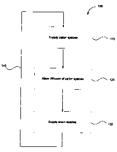
[022] Referring to Figure 1, there is illustrated a method 100 for producing a
thin film
using plasma enhanced chemical vapour deposition. At step 110, a cation
species is
supplied to a substrate (i.e. sample) region (for thin film growth on a
substrate) with no, or
a relatively low flux of a plasma based anion species being present. At step
120, the
cations are allowed sufficient time to diffuse on the film/substrate. This can
be as part of
the time duration when supplying the cations, or as a separate intermediate
time delay step.
In this way the cation is resident on a film surface long enough to be able to
diffuse to an
energetically favourable site for good film growth. This lateral growth can
result in good
quality thin film material at relatively low film growth temperatures. Then at
step 130 the
cation species flux is significantly reduced or stopped and a plasma based
anion species is
supplied to the substrate region. The process can be repeated at step 140, as
required if
necessary, to a obtain a desired film thickness. Thus, method 100 provides a
means for
migration enhanced epitaxy in a plasma enhanced chemical vapour deposition
system.
[023] This novel technique is ideally suited to the growth of some compound
semiconductors, such as group III metal nitrides, rare earth nitrides, other
nitride
compound species and oxide compound species. With the introduction of
migration
enhanced epitaxy it is also possible to vary the growth conditions for a
cation species (e.g.
CA 02653581 2009-02-11
-5-
Group III metals including Boron, Aluminium, Gallium, Indium, Thallium, etc.)
and an
anion species (e.g. Nitrogen, Oxygen, etc.) separately, which can lead to some
gains in
improved precursor delivery. Obviously, a wide variety of other reactant
species can be
used.
[024] In a specific but non-limiting example, the method of achieving
migration
enhanced epitaxy can be applied to known RPECVD based film growth of group III
nitride
films, for example the systems described in International Patent Publications
W02006/034540 and W02003/097532, of which the present inventor is a co-
inventor,
which are incorporated herein by reference.
[025] An acronym that describes this technique is ME-RPECVD, or migration
enhanced
RPECVD. However, RPECVD reactors are also referred to as afterglow reactors,
so that
the acronym MEAGIow (migration enhanced afterglow), is preferred. It should be
noted
that the technique also can be applied to PECVD systems.
[026] In a specific illustrative example, known RPECVD based film growth
methods can
be generally used for the growth of good quality gallium nitride films at
growth rates of
less than 150 nm/hour. The achievement of higher growth rates is desirable to
lower device
deposition time, and to thereby allow RPECVD to be more competitive with MOCVD
where growth rates as high as 2-3 m/hr can be achieved for good quality film
growth.
[027] However, achieving higher growth rates for the RPECVD growth of gallium
nitride, for instance, is dependent on having a plasma source that produces a
higher
number of active nitrogen based species in the gas phase. Hence, a more
efficient plasma
source, capable of increasing the film growth rate, will incur the problem of
a higher rate
of dust formation. The low temperature growth by RPECVD of good crystalline
quality
GaN, has also been found to be less consistent than would be desirable. By
using a
MEAGIow system capable of applying the aforementioned method, both these
problems
can be addressed.
[028] In a particular illustrative example, a relatively short pulse of the
gallium precursor
material, trimethylgallium, is delivered at a much higher delivery rate than
for normal
RPECVD, which would cause the formation of excess gallium on the sample
surface. The
CA 02653581 2009-02-11
-6-
pulse is of sufficient duration to allow diffusion of the gallium species at
the sample
surface. A pulse of a remote nitrogen or ammonia plasma can then follow the
pulse of
metalorganic, to supply the nitrogen species used by RPECVD for film growth.
In this way
the reactant species are in the gas phase at separate times and dust formation
is reduced,
while the utilisation of higher source flow fluxes allows faster growth rates
to be achieved.
In a MEAGIow reactor higher film crystallinity than is observed for RPECVD can
be
achieved as a result of the diffusion of the group III metal component on the
substrate
surface prior to the delivery of the active nitrogen species.
[029] Thus, the MEAGIow reactor can be used to reduce the formation of dust
during
thin film growth by relatively high pressure film growth techniques, for
example, operating
approximately over a range of I mTorr to 10 Torr, compared to MBE (molecular
beam
epitaxy) which operates over a range of 0.000001 mTorr to 0.1 mTorr.
[030] Referring to Figure 2, there is illustrated a schematic of an example
plasma
processing reactor that provides a MEAGIow reactor 200. Main chamber 210 is
where
reactions between chemical species occurs. A plasma power source 215 creates a
contained
plasma where plasma species are supplied by plasma supply lines 220. Plasma
power
source 215 can be cooled by water inlet/outlet 225. Main chamber 210 contains
a substrate
that can be adjusted in height by pneumatic sample lift 230. The region below
the substrate
can be connected to pump line 235 to assist in creating a vacuum in main
chamber 210.
Main chamber 210 is connected to load lock 240 via gate valve 245. Main
chamber 210 is
also connected to conflat cross 250 via gate valve 255.
[031] An optical omission spectrometer optical fibre 260 can be introduced
into main
chamber 210 for diagnostic purposes. A further water inlet/outlet 265 and a
purge valve
270 are associated with main chamber 210. A metaloraganic inlet 275 supplies a
metalorganic species to main chamber 210. A bypass pump 280 is also connected
to
metalorganic inlet line 275.
[032] Load lock 240 is connected to dry pump 285 with associated water
inlet/outlet 290.
A transfer arm 295 is associated with load lock 240. Wide range gauge 300 can
be used to
measure the pressure on dry pump 285 side of load lock 240. Throttle valve 305
and filter
310 connect pump line 235 to dry pump 285.
CA 02653581 2009-02-11
-7-
[033] Conflat cross 250 is connected to a turbo pump 315 which is connected to
a
backing pump 320 via filter 325 and electrical isolation valve 330. Backing
pump 320 and
dry pump 285 exhaust gas into exhaust line 335. RGA 340 is connected to
conflat cross
250 which can also be provided with an associated wide range gauge 345.
[034] Referring to Figure 3, there is illustrated a schematic of an example
main chamber
of a plasma processing reactor providing part of a MEAGIow reactor. Main
chamber 400
includes housing 405 enabling a vacuum to be created in main chamber 400. Gas
flow
outlets 410 and 415 are connected to a vacuum system to remove gases from main
chamber 400. Metalorganic species 430 is introduced internally into region 460
of main
chamber 400 via metalorganic inlet 420, which is connected to "shower head"
feed 425.
Shower head feed 425 directs metalorganic species 430 onto a substrate which
is held by
or placed on substrate holder 435. Substrate holder 435 is supported by, and
can be heated
by pedestal 440.
[035] A hollow cathode 445 is provided above a ground grid 450. Gas flows
through
hollow cathode 445 and ground grid 450 from plasma creation region 455 into
reaction
region 460, being in the vicinity of the substrate on substrate holder 435.
[036] Anode 465 is supported by insulator supports 470 and attached to power
line 475.
A plasma based species is introduced into plasma creation region 455 via
plasma gas inlet
480. A plasma can thus be created in region 455 that diffuses into region 460
to react with
metalorganic species 430 on the substrate.
[037] A standard capacitively coupled plasma can be formed between anode 465
and
hollow cathode 445. This can be achieved by RF excitation of the anode 465
from RF
power supply line 475. In this case, the plasma itself can act as a virtual
anode, or by DC
excitation of anode 465. There is some evidence to suggest that DC excitation
results in
higher density plasmas. In the holes in cathode 445, at certain gas flows and
pressures,
dependent on the geometry of the holes, a very strong additional plasma can be
achieved
due to the hollow cathode effect. Any additional plasma created by the hollow
cathode
effect is contained well above the substrate/sample by ground grid 450, since
energetic
ions can be damaging to the thin film during film growth.
CA 02653581 2009-02-11
-8-
[038] Referring to Figure 4, there is illustrated a schematic of an example
"shower head"
feed 425 that can be used in MEAGIow reactor chamber 400. Shower head feed 425
distributes metalorganic species to the substrate/sample. The shower head feed
425 can be
located relatively close to the substrate/sample holder 435 as compared to a
normal
RPECVD system configuration. A preferred hole dispersion pattern for the
shower head
feed 425 is illustrated in Figure 4. Holes 428 are formed in a surface of the
shower head
feed 425 to release metalorganic species. Holes 428 direct metalorganic
species 430 onto
the substrate/sample. For the purposes of illustration only, a sample holder
recess 485 and
a sample holder lip 490, being part of substrate holder 435, are illustrated
in relative
position to shower head feed 425 and holes 428. A typical sample/substrate
would be
placed within sample holder recess 485. Preferably, substrate holder 435 is
rotated about a
longitudinal axis so that a substrate/sample rotates under shower head feed
425 and so that
metalorganic species is evenly distributed on the substrate/sample.
[039] For the deposition of group III nitride semiconductor thin films by
ordinary known
RPECVD methods, the inventor has found that RF generated plasma supplies
operating at
13.56 MHz have not proven particularly effective, with too much dust
production being
evident. In contrast, 2.45 GHz microwave plasma systems have proven to be more
effective with substantially less dust production. It has been reported that
for microwave
generated plasmas less energy is required to sustain an electron-ion pair. For
argon
plasmas it has been estimated that 2-7 times less power per electron-ion pair
is required at
2.45 GHz than at RF frequencies - dependent upon the discharge conditions.
Hence, there
is expected a greater degree of ionisation in a microwave generated plasma
compared to an
RF generated plasma for a given applied power. The excess energy used to
generate an
electron-ion pair for the RF case eventually devolves to heat, which would
promote gas
phase reactions and the formation of dust during ordinary RPECVD film growth.
However, the electron density (and hence the degree of ionisation - or
electron-ion
density) of an RF generated plasma is highly dependent on the means of
generation.
Capacitively coupled RF plasma generation (commonly used for semiconductor
processing) is the least effective means, with electron-ion densities
typically around 109 to
1010 cm-3. While inductively coupled RF plasmas can typically have densities
of 101, to
1012 cm"3. This is similar to the densities achieved by microwave plasma
systems, though
typically less power is used in the case of the microwave source to achieve
such densities.
CA 02653581 2009-02-11
-9-
Other types of RF, or lower frequency plasmas, which utilise resonance
characteristics can
be even denser. RF, and lower frequency, hollow cathode plasma sources can
also produce
high densities of ion-electron pairs.
[040] For PECVD based processes, where substrates are in direct contact with
the
plasma, a high level of ionic species is usually a positive for plasma
processes. This is also
the case for RPECVD, and it is important to note that although the active
species used in
RPECVD film growth is not the ionic species, a greater degree of ionisation
within the
plasma will generally translate into a denser concentration of neutral species
in the
afterglow region. Some RF based plasma systems may be suitable for RPECVD, if
heating
of the metalorganic reactants in the gas phase by the plasma source can be
avoided.
[041] In the case of RPECVD using a nitrogen gas source for the plasma, the
lowest
excited state of molecular nitrogen has an extremely long radiative lifetime,
estimated to
be as high as 2 seconds by some groups and is a major contributing species to
nitride film
growth by RPECVD. For a hollow cathode source this lowest excited molecular
nitrogen
state has been observed to be present at densities as high as about 4.9 x 10"
cm-'. In
conventional RPECVD, however, it is known that collisions with some impurity
species,
including CH4, is gas kinetic and will rapidly quench this form of neutral
nitrogen at a rate
of up to - 1000 times higher than collisions with molecular nitrogen.
[042] For RPECVD film growth where excited nitrogen molecular neutrals and
metalorganic species are present at the same time in the growth system, a
notable reduction
in the active nitrogen that reaches the substrate can be expected due to
quenching caused
by collisions with these methyl group species, resulting in a lower then
expected growth
rate. Gas phase reactions due to the interaction of the metalorganic with the
active neutral
nitrogen can also be expected. The inventor has observed a strong secondary
light emission
(chemiluminescence) in the far downstream afterglow of a microwave generated
nitrogen
plasma when metalorganic is introduced into the system, which suggests that
such gas
phase interactions are in progress. Using a migration enhanced configuration,
where the
metalorganic is not introduced at the same time as the active nitrogen should
therefore
allow a greater proportion of active species to reach the substrate to
participate in film
growth.
CA 02653581 2009-02-11
-10-
[043] Microwave based plasma generation systems are electrodeless, a strong
electromagnetic field in a resonant cavity leads to gas breakdown. A
dielectric window is
used to transmit the electromagnetic field into the gas system where the
plasma is
generated, usually at low pressure. It has been found that plasma interaction
with the
dielectric window can cause contamination of the plasma by species being
etched from the
window. A lengthy surface passivation cycle, taking as long as two days, in a
well
evacuated vacuum system that has no exposure to atmosphere is needed to create
a nitride
layer on the window to overcome this problem, as is outlined in International
Patent
Publication W02006/034540. Because of the relatively short wavelengths of
microwave
sources and the need to have dimensional cavities to sustain the plasma, it is
also quite
difficult to scale microwave sources for film deposition over large areas.
[044] Although there are some advantages of the use of microwave plasma
sources, the
use of other sources, such as hollow cathode plasma sources, should allow for
easier
plasma source scalability and for reduced concern about contamination from
windows. The
use of a migration enhanced growth scenario would allow other plasma sources
to be used
without concern for gas heating which can result in enhanced dust formation
problems. In
particular, hollow cathode sources, which do not employ dielectric windows
could be used.
[045] Another advantage of a microwave plasma generation system is the ability
to
sustain the plasma over a very wide range of pressure. The inventor has been
able to
sustain a microwave generated nitrogen plasma over a 22 Torr to 10 mTorr range
using a
system capable of delivering approximately 600 W of power. Other RF and lower
frequency (e.g. DC) generated plasmas do not generally have such a broad range
of
operating pressure. Again, using a migration enhanced methodology allows
separate
conditions to be used for the application of the metalorganic and the plasma,
so that the
chamber pressure for the delivery of the active nitrogen can be tailored to
the plasma
source used. To prevent high energy neutral species (such as atomic nitrogen)
from
reaching the substrate (which can happen at too low a growth pressure) the
flow rate from
the plasma source can be reduced and the distance from the plasma to the
substrate can be
adjusted, instead of adjusting the chamber pressure. This can provide a
balance between
having a high density of low energy active neutral species for film growth,
while
minimising the presence of higher energy damaging species, which can affect
film quality
and reduce the growth rate through etching.
CA 02653581 2009-02-11
-11-
[046] The delivery of the metalorganic for a migration enhanced film growth
regime can
be optimised to enable a higher delivery rate to the substrate. The gas head
for the
metalorganic can be positioned quite close to the substrate holder, and
relatively low
delivery pressures can be used to increase the utilisation of the
metalorganic. The
requirement for uniform radial and axial delivery in the chamber, necessary
during
conventional RPECVD film growth, can be relaxed for film growth in a MEAGIow
reactor, with only radial uniformity being a necessary condition for design of
the
metalorganic delivery head.
[047] During normal RPECVD film growth, rotation is used to "smooth out" small
non-
uniformities that occur axially, but because film growth is continuous during
the process,
uniform conditions are required to maintain uniform film properties that would
otherwise
be grown into the film. In contrast, for a MEAGIow reactor, the film growth
only occurs
during the application of the plasma. Metalorganic delivery can therefore
occur along a
radius of the substrate holder so long as rotation of the substrate under that
radius is rapid
enough to provide uniform coverage of the substrate by the metal while the
plasma source
is off. The configuration of the metalorganic vapour delivery head can
therefore be greatly
simplified. Continued rotation while the plasma is on and the metalorganic is
off ensures
that any shadowing by the delivery head is not detrimental in terms of
ensuring migration
enhanced epitaxy occurs, and a uniform layer is deposited over the plasma on
period.
[048] Referring to Figure 5A, there is shown by way of example only an image
of an
instance of migration enhanced type growth for an InN film grown in a RPECVD
type
reactor. The substrate is shown at the bottom of the figure, above which is
the largely
polycrystalline film, shown at roughly a 30 degree angle to the horizontal
with columinar
growth typical of a hexagonal crystal structure being evident. At the top
surface region of
the film, however, the columinar crystals are terminated with an apparently
single crystal
layer where lateral film growth has been greatly enhanced. In contrast,
referring to Figure
5B, there is shown by way of example only an image of an instance of non-
migration
enhanced type growth for an InN film grown in a RPECVD type reactor. There is
no
evidence of a top laterally grown layer.
CA 02653581 2009-02-11
-12-
[049] In summary, there has been described a method and a plasma reactor
device for
achieving an increased rate of thin film growth and reducing dust formation
problems
compared to conventional PECVD or RPECVD systems and methods. A reduction of
dust
formation problems and improved crystallinity due to improved lateral growth
can be
expected in MEAGIow compared to conventional RPECVD. The film growth rate
improvement for MEAGIow can occur because of the use of higher fluxes of the
precursor
materials, without dust formation problems. Growth rate improvement for
MEAGIow is
also expected because the active neutral plasma species is not consumed by
impurities in
the gas phase, in particular by a metalorganic precursor material, i.e. more
of the active
species make it to the substrate region for a given flux of these active
species.
[050] For MEAGIow, plasma sources other than RF or microwave plasma sources
can be
used because gas heating by the plasma source is less of an issue (powder
production is
reduced regardless). Because the conditions for delivery of a metalorganic
cation and a
plasma generated anion are not congruent the conditions for the delivery of
each precursor
can be independently optimised. This also enables a simplified metalorganic
delivery head
to be used for MEAGIow compared to RPECVD, or MOCVD. The chamber, pressure
during the delivery of the metalorganic cation can also be greatly reduced so
that the use of
a carrier gas with the metalorganic (as is typically used for RPECVD, MOCVD
and
PECVD) is not necessary. The metalorganic can be delivered as a pure vapour
using a
much simplified gas delivery system for which carrier mixing with the
metalorganic is not
required.
[051] Optional embodiments of the present invention may also be said to
broadly consist
in the parts, elements and features referred to or indicated herein,
individually or
collectively, in any or all combinations of two or more of the parts, elements
or features,
and wherein specific integers are mentioned herein which have known
equivalents in the
art to which the invention relates, such known equivalents are deemed to be
incorporated
herein as if individually set forth.
[052] Although a preferred embodiment has been described in detail, it should
be
understood that various changes, substitutions, and alterations can be made by
one of
ordinary skill in the art without departing from the scope of the present
invention.