Note : Les descriptions sont présentées dans la langue officielle dans laquelle elles ont été soumises.
CA 02658578 2009-01-16
WO 2008/105804 PCT/US2007/016334
ORGANIC OPTOELECTRONIC DEVICE ELECTRODES WITH NANOTUBES
RELATED APPLICATIONS
[0001] This application claims the benefit of U.S. Provisional Application No.
60/831,710 filed July 18, 2006, the disclosure of which is incorporated herein
by reference in
its entirety.
GOVERNMENT RIGHTS
[0002] This invention was made with U.S. Government support under Contract No.
N66001-04-1-8902 awarded by the Defense Advance Research Projects Agency
MolYApps
Program. The government has certain rights in this invention.
JOINT RESEARCH AGREEMENT
[0003] The claimed invention was made by, on behalf of, and/or in connection
with
one or more of the following parties to a joint university corporation
research agreement:
Princeton University, The University of Southern California, the Universal
Display
Corporation, and the Global Photonic Energy Corporation. The agreement was in
effect on
and before the date the claimed invention was made, and the claimed invention
was made as
a result of activities undertaken within the scope of the agreement.
1
CA 02658578 2009-01-16
WO 2008/105804 PCT/US2007/016334
[0004] The present invention relates to organic optoelectronic devices. More
specifically, it relates to organic optoelectronic devices incorporating
nanotubes.
BACKGROUND
[0005] Optoelectronic devices rely on the optical and electronic properties of
materials to either produce or detect electromagnetic radiation electronically
or to generate
electricity from ambient electromagnetic radiation. Examples of organic
optoelectronic
devices include organic light emitting devices (OLEDs), organic
phototransistors, organic
photovoltaic (PV) cells, and organic photodetectors.
[0006] As used herein, the term "organic" includes polymeric materials as well
as
small molecule organic materials that may be used to fabricate organic
optoelectronic
devices. "Small molecule" refers to any organic material that is not a
polymer, and "small
molecules" may actually be quite large. Small molecules may include repeat
units in some
circumstances. In general, a small molecule has a well-defined chemical
formula with a
single molecular weight, whereas a polymer has a chemical formula and a
molecular weight
that may vary from molecule to molecule.
[0007] OLEDs make use of thin organic films that emit light when voltage is
applied
across the device. OLEDs are becoming an increasingly interesting technology
for use in
applications such as flat panel displays, illumination, and backlighting.
Several OLED
materials and configurations are described in U.S. Patent Nos. 5,844,363,
6,303,238, and
5,707,745, which are incorporated herein by reference in their entirety.
[0008] OLED devices are generally intended to emit light through at least one
electrode, and one or more transparent electrodes may be useful in an organic
optoelectronic
devices. For example, an electrode may comprise a transparent electrode
material, such as
indium tin oxide (ITO). Transparent top electrodes are further described in
U.S. Patent Nos.
5,703,436 and 5,707,745, which are incorporated by reference in their
entireties. For a device
intended to emit light only through the bottom electrode, the top electrode
does not need to be
transparent, and may comprise a thick and reflective metal layer having a high
electrical
conductivity. Similarly, for a device intended to emit light only through the
top electrode, the
bottom electrode may be opaque and / or reflective. Where an electrode does
not need to be
transparent, using a thicker layer may provide better conductivity, and using
a reflective
electrode may increase the amount of light emitted through the other
electrode, by reflecting
2
CA 02658578 2009-01-16
WO 2008/105804 PCT/US2007/016334
light back towards the transparent electrode. Fully transparent devices may
also be
fabricated, where both electrodes are transparent. Side emitting OLEDs may
also be
fabricated, and one or both electrodes may be opaque or reflective in such
devices.
[0009] Photosensitive optoelectronic devices convert electromagnetic radiation
into
an electrical signal or electricity. An organic photosensitive device
typically includes at least
one photoactive region in which light is absorbed to form an exciton, which
may
subsequently dissociate into an electron and a hole. The "photoactive region"
is a portion of
a photosensitive device that absorbs electromagnetic radiation to generate
excitons that may
dissociate in order to generate an electrical current. Solar cells, also
called photovoltaic
("PV") devices, are a type of photosensitive optoelectronic device that is
specifically used to
generate electrical power. Photoconductor cells are a type of photosensitive
optoelectronic
device that are used in conjunction with signal detection circuitry which
monitors the
resistance of the device to detect changes due to absorbed light.
Photodetectors, which may
receive an applied bias voltage, are a type of photosensitive optoelectronic
device that are
used. in conjunction with current detecting circuits which measures the
current generated
when the photodetector is exposed to electromagnetic radiation. Organic
photosensitive
devices, including their general construction, characteristics, materials, and
features, are
further described in U.S. Patent No. 6,657,378 to Forrest et al., U.S. Patent
No. 6,580,027 to
Forrest et al., and U.S. Patent No. 6,352,777 to Bulovic et al., each of which
is incorporated
herein by reference in its entirety.
[0010] As used herein, "top" means furthest away from the substrate, while
"bottom"
means closest to the substrate. For example, for a device having two
electrodes, the bottom
electrode is the electrode closest to the substrate, and is generally the
first electrode
fabricated. The bottom electrode has two surfaces, a bottom surface closest to
the substrate,
and a top surface further away from the substrate. Where a first layer is
described as
"disposed over" a second layer, the first layer is disposed further away from
substrate. There
may be other layers between the first and second layer, unless it is specified
that the first
layer is "in physical contact with" the second layer. For example, a cathode
may be
described as "disposed over" an anode, even though there are various organic
layers in
between.
SUMMARY OF THE INVENTION
3
CA 02658578 2009-01-16
WO 2008/105804 PCT/US2007/016334
[0011] A layer for use in an organic optoelectronic device is provided. The
layer
includes a thin film of single-wall carbon nanotubes. The film may be
deposited on a
substrate of the device by using an elastomeric stamp. The film may be
enhanced by spin-
coating a smoothing layer on the film and/or doping the film to enhance
conductivity. When
the layer is used as an electrode, it may have a conductivity, transparency,
and other features
comparable to conventional electrodes typically used in optoelectronic
devices.
BRIEF DESCRIPTION OF THE DRAWINGS
[0012] FIG. 1 shows an exemplary organic light emitting device.
[0013] FIG. 2 shows an exemplary organic photosensitive device.
[0014] FIG. 3A shows a porous alumina filtration membrane used to fabricate a
thin
film of nanotubes.
100151 FIG. 3B shows a thin film of nanotubes.
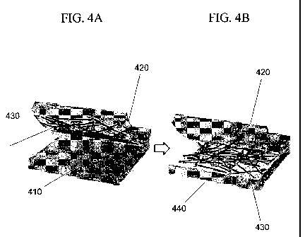
[0016] FIGS. 4A-4B show a thin film of nanotubes transferred to a substrate
using an
elastomeric stamp.
[0017] FIG. 4C shows a transparent 40 nm thick single-wall nanotube film on a
2"
diameter glass substrate.
[0018] FIG. 4D shows a flexed single-wall nanotube film on a polyester sheet.
[0019] FIG. 5A is a perspective view SEM image of a thin film of HiPCO single-
wall
nanotubes.
[0020] FIG. 5B is a perspective view SEM image of a thin film of P3 single-
wall
nanotubes.
[0021] FIG. 5C shows a top view SEM image of the nanotube film illustrated in
FIG.
5A.
[0022] FIG. 5D shows a top view SEM image of the nanotube film illustrated in
FIG.
5B.
[0023] FIG. 5E shows an enlarged view of the image shown in FIG. 5C.
[0024] 5F shows an enlarged view of the image shown in FIG. 5D.
4
CA 02658578 2009-01-16
WO 2008/105804 PCT/US2007/016334
[0025] FIG. 5G shows the resistance at various transparencies for HiPCO and P3
nanotube films.
[0026] FIG. 6A shows an AFM image of a P3 SWNT film on glass.
[0027] FIG. 6B shows an AFM image of a P3 SWNT film after spin-coating.
[0028] FIG. 6C shows an AFM image of a layer of a standard ITO film.
[0029] FIG. 7A shows sheet resistance of P3 SWNT films as a function of film
thickness.
[0030] FIG. 7B shows the electrical conductivity of P3 SWNT films as a
function of
film thicknesses.
[0031] FIG. 8A shows the transmittance spectra of P3 SWNT films.
[0032] FIG. 8B shows sheet resistance of P3 SWNT films as a function of
temperature.
[0033] FIG. 9A shows four-probe I-V curves of P3 SWNT films before and after
SOC12 incubation.
[0034] FIG. 9B shows the transmittance spectra of P3 SWNT films before and
after
SOC12 treatment.
[0035] FIG. 10A shows a schematic diagram of an optoelectronic device having a
SVdNT film layer.
[0036] FIG. l OB shows an energy level diagram of the device illustrated in
FIG. 10A.
[0037] FIG. l OC shows a photograph of an optoelectronic device having a SWNT
film layer.
[0038] FIG. 11A shows the photoluminescence spectrum of Alq3.
[0039] FIG. .11B shows the current-voltage curve of an OLED having a SWNT film
layer.
[0040] FIG. 11 C shows the brightness of an OLED having a SWNT film layer as a
function of the voltage bias.
[0041] FIG. 11D shows the quantum efficiency of an OLED having a SWNT film
layer as a function of voltage bias.
CA 02658578 2009-01-16
WO 2008/105804 PCT/US2007/016334
[0042] FIG. 12 shows optical transmittance spectra of SWNT and ITO transparent
electrodes fabricated on plastic.
[0043] FIG. 13 shows current-voltage curves for devices with
CuPc/C6o/bathocuproine photoactive regions on SWNT and ITO electrodes.
DETAILED DESCRIPTION
[0044] FIG. 1 shows an exemplary organic light emitting device 100. The
figures are
not necessarily drawn to scale. The device 100 may include a substrate 110, an
anode 115, a
hole injection layer 120, a hole transport layer 125, an electron blocking
layer 130, an
emissive layer 135, a hole blocking layer 140, an electron transport layer
145, an electron
injection layer 150, a protective layer 155, and a cathode 160. Cathode 160
may be a
compound cathode having a first conductive layer 162 and a second conductive
layer 164.
Device 100 may be fabricated by depositing the layers described, in order.
[0045] FIG. 2 shows an exemplary organic photosensitive device 200. A
photoactive
region 250 comprises a donor-acceptor heterojunction. Device 200 comprises an
anode 220,
an anode smoothing layer 222, a donor 252, an acceptor 254, an exciton
blocking layer
("EBL") 256, and a cathode 270, over a substrate 210. The devices as
illustrated may be
connected to an element 290. If the device is a photovoltaic device, element
290 is a resistive
load which consumes or stores power. If the device is a photodetector, element
290 is a
current detecting circuit which measures the current generated when the
photodetector is
exposed to light, and which may apply a bias to the device (as described for
example in
Published U.S. Patent Application 2005-0110007 Al, published May 26, 2005 to
Forrest et
al.). Unless otherwise stated, each of these arrangements and modifications
may be used for
the devices in each of the drawings and embodiments disclosed herein. If a
photoactive
region includes a mixed layer or bulk layers and one or both of the donor and
acceptor layers,
the photoactive region is said to include a "hybrid" heterojunction. For
additional
explanation of hybrid heterojunctions, Published U.S. Patent Application
2005/0224113 Al,
entitled "High efficiency organic photovoltaic cells employing hybridized
mixed-planar
heterojunctions" by Jiangeng Xue et al., published October 13, 2005, is hereby
incorporated
by reference.
[0046] Substrates 110, 210 on which optoelectronic devices are fabricated may
comprise any suitable substrate material that provides desired structural
properties.
6
CA 02658578 2009-01-16
WO 2008/105804 PCT/US2007/016334
Substrates used with the invention may be flexible or rigid and transparent,
translucent or
opaque. Exemplary substrate materials include plastic, glass, metal foils, and
semiconductor
materials. For example, a substrate may comprise a silicon wafer upon which
circuits are
fabricated, capable of controlling devices subsequently deposited on the
substrate. Other
substrates may be used. The material and thickness of the substrate may be
chosen to obtain
desired structural and optical properties.
[0047] The term "electrode" is used herein to refer to a layer that provides a
medium
for delivering photo-generated current to an external circuit or providing a
current or voltage
to a device. As illustrated in FIGS. 1 and 2, anodes 115, 220 and cathodes
160, 270 are
exemplary electrodes. Electrodes may be composed of metals or "metal
substitutes." Herein
the term "metal" is used to embrace both materials composed of an elementally
pure metal,
and also metal alloys which are materials composed of two or more elementally
pure metals.
The term "metal substitute" refers to a material that is not a metal within
the normal
definition, but which has the metal-like properties such as conductivity, such
as doped wide-
bandgap semiconductors, degenerate semiconductors, conducting oxides, and
conductive
polymers. Electrodes may comprise a single layer or multiple layers (a
"compound"
electrode), may be transparent, semi-transparent, or opaque. Examples of
electrodes and
electrode materials include those disclosed in U.S. Patent No. 6,352,777 to
Bulovic et al., and
U.S. Patent No. 6,420,031, to Parthasarathy, et al., each of which is
incorporated herein by
reference for disclosure of these respective features. As used herein, an
electrode or other
layer is said to be "transparent" if it transmits at least 50% of the ambient
electromagnetic
radiation in a relevant wavelength.
[0048] In some configurations, devices according to the present invention may
include one or more conventional anodes in addition to the electrodes and
other layers
described herein. Anodes used in the present invention may comprise any
suitable anode
material that is sufficiently conductive to transport holes. Exemplary anode
materials include
conductive metal oxides, such as indium tin oxide (ITO) and indium zinc oxide
(IZO),
aluminum zinc oxide (AlZnO), and metals. Anodes may be sufficiently
transparent to create
a bottom-emitting device. An exemplary transparent substrate and anode
combination is
commercially available ITO (anode) deposited on glass or plastic (substrate).
A flexible and
transparent substrate-anode combination is disclosed in United States Patent
Nos. 5,844,363
and 6,602,540 B2, which are incorporated by reference in their entireties.
Anodes may be
opaque and/or reflective. A reflective anode may be preferred for some top-
emitting devices,
7
CA 02658578 2009-01-16
WO 2008/105804 PCT/US2007/016334
to increase the amount of light emitted from the top of the device. The
material and thickness
of an anode may be chosen to obtain desired conductive and optical properties.
For a
transparent anode, there may be a range of thickness for a particular material
that is thick
enough to provide the desired conductivity, yet thin enough to provide the
desired degree of
transparency. Other anode materials and structures may be used.
[0049] In some configurations, devices according to the present invention may
include one or more conventional cathodes in addition to the electrodes and
other layers
described herein. Cathodes used with the present invention may comprise any
suitable
material or combination of materials known to the art, such that the cathode
is capable of
conducting electrons. Cathodes may be transparent or opaque, and may be
reflective. Metals
and metal oxides are examples of suitable cathode materials. Cathodes may be a
single layer,
or may have a compound structure. For example, FIG. 1 shows a compound cathode
160
having a thin metal layer 162 and a thicker conductive metal oxide layer 164.
In a compound
cathode, preferred materials for the thicker layer 164 include ITO, IZO, and
other materials
known to the art. U.S. Patent Nos. 5,703,436, 5,707,745, 6,548,956 B2 and
6,576,134 B2,
which are incorporated by reference in their entireties, disclose other
exemplary cathodes.
Other cathode materials and structures may be used.
[0050] Various other layers may be present in optoelectronic devices according
to the
invention. Transport layers may be used to transport charge carriers from one
layer to
another, such as from an electrode or an injection layer to the emissive
layer. Examples of
hole and electron transport layers are disclosed in U.S. Patent Application
Pub. No. 2003-
0230980 to Forrest et al., which is incorporated by reference in its entirety.
Other hole and/or
electron transport layers may be used. Injection layer materials may be
distinguished from
conventional transporting materials in that such materials may have a charge
carrier
conductivity that is substantially less than the conductivity of conventional
transporting
materials. Injection layers may also perform a charge transport function.
Detailed
descriptions and examples of injection layers and transport layers are given
in U.S. Patent
No. 7,053,547 to Lu et al., which is incorporated herein by reference it its
entirety. More
examples of injection layers are provided in U.S. Patent Application Serial
No. 09/931,948 to
Lu et al., which is incorporated by reference in its entirety. Blocking layers
may provide a
barrier that significantly inhibits transport of charge carriers and/or
excitons through the
device, without necessarily completely blocking the charge carriers and/or
excitons. The
theory and use of blocking layers, and further examples of specific blocking
layers, are
8
CA 02658578 2009-01-16
WO 2008/105804 PCT/US2007/016334
described in more detail in U.S. Patent No. 6,097,147, U.S. Patent Application
Publication
No. 2003-0230980 to Forrest et al., and U.S. Patent No. 6,451,415 to Forrest
et al., which are
incorporated by reference in their entireties. Additional background
explanation of EBLs
may also be found in Peumans et al., "Efficient photon harvesting at high
optical intensities
in ultrathin organic double-heterostructure photovoltaic diodes," Applied
Physics Letters 76,
2650-52 (2000).
[0051] In emissive devices such as OLEDs, an emissive layer may include an
organic
material capable of emitting light when a current is passed through the layer.
Preferably, an
emissive layer contains a phosphorescent emissive material, although
fluorescent emissive
materials may also be used. An emissive layer may include a plurality, of
emissive materials
capable of, in combination, emitting a desired spectrum of light. Examples of
phosphorescent emissive materials include Ir(ppy)3. Examples of fluorescent
emissive
materials include DCM and DMQA. Examples of host materials include Alq3i CBP
and
mCP. Further examples of emissive and host materials are disclosed in U.S.
Patent No.
6,303,238 to Thompson et al., which is incorporated by, reference in its
entirety. Other
emissive layer materials and structures may be used.
[0052] An organic photosensitive optoelectronic device may include charge
transfer
layers, electrodes, and/or charge recombination zones. A charge transfer layer
may be
organic or inorganic, and may or may not be photoconductively active. A charge
transfer
layer is similar to an electrode, but does not have an electrical connection
external to the
device and only delivers charge carriers from one subsection of an
optoelectronic device to
the adjacent subsection. A charge recombination zone is similar to a charge
transfer layer,
but allows for the recombination of electrons and holes between adjacent
subsections of an
optoelectronic device. A charge recombination zone may include semi-
transparent metal or
metal substitute recombination centers comprising nanoclusters, nanoparticles,
and/or
nanorods, as described for example in U.S. Patent No. 6,657,378 to Forrest et
al.; Published
U.S. Patent Application 2006-0032529 Al, entitled "Organic Photosensitive
Devices" by
Rand et al., published February 16, 2006; and Published U.S. Patent
Application 2006-
0027802 Al, entitled "Stacked Organic Photosensitive Devices" by Forrest et
al., published
February 9, 2006; each incorporated herein by reference for its disclosure of
recombination
zone materials and structures. An electrode or charge transfer layer may serve
as a Schottky
contact.
9
CA 02658578 2009-01-16
WO 2008/105804 PCT/US2007/016334
[0053] Protective and/or sinoothing layers may be used in organic
optoelectronic
devices. A more detailed description of protective layers may be found in U.S.
Patent
Application Serial No. 09/931,948 to Lu et al., which is incorporated by
reference in its
entirety. Smoothing layers are described in U.S. Patent 6,657,378 to Forrest
et al., which is
incorporated by reference in its entirety.
[0054] The performance of optoelectronic devices may be enhanced by
incorporating
carbon nanotubes (CNTs) into polymer matrices as a dopant material. Generally,
CNTs are
seamless cylindrical arrangements of carbon atoms. A single-wall carbon
nanotube (SWNT)
is a one-atom thick sheet of graphite (graphene) in a cylindrical
configuration. A SWNT
typically has a diameter of the order of a nanometer, and can have a length-to-
diameter ratio
of over 10,000. Multi-wall nanotubes typically are of two types. In the first
type, a graphene
sheet is arranged in a rolled cylindrical configuration, where the length of
the sheet is longer
than the circumference of the resulting nanotube. That is, the sheet overlaps
itself, and can
form multiple layers on and within the nanotube. In the second type, multiple
SWNT
structures of different radii are arranged concentrically around a common long
axis.
[0055] It has been found that the combination of CNTs with polymers may
reinforce
polymer films and/or also introduce new electronic properties based on
morphological
modification or electronic interaction between the two components. The effect
of CNT
doping has been investigated by embedding CNT powders in the emission,
electron-transport
and hole-transport layers of OLEDs. By introducing additional energy levels or
forming
carrier traps in the host polymers, the CNT dopant can selectively facilitate
or block the
transport of charge carriers, and may improve OLED performance at optimized
dopant
concentrations.
[0056] Continuous CNT films may complement indium-tin oxide (ITO) for certain
applications, including organic light emitting diodes and organic photovoltaic
(OPV) devices.
For example, CNT films may be bent to acute angles without fracture; in
contrast, ITO films
typically are not as flexible. In addition, while carbon is the most abundant
element in
nature, the world-wide production of indium is limited, which may soon cause
difficulty in
meeting an ever-increasing demand for large-area transparent conductive
electrodes. CNT
films also may offer additional advantages such as tunable electronic
properties through
chemical treatment and enhanced carrier injection owing to the large surface
area and field-
enhanced effect at the nanotube tips and surfaces.
CA 02658578 2009-01-16
WO 2008/105804 PCT/US2007/016334
[0057] Carbon nanotubes may be single-walled or multi-walled. Multi-walled
nanotubes contain multiple layers of graphite arranged concentrically in a
tube. Generally,
single-walled nanotubes (SWNTs) exhibit better electrical properties than
multi-walled
nanotubes. SWNTs commercially available in bulk quantity are generally
manufactured
using either a high-pressure carbon monoxide (HiPCO) process (such as HiPCO
nanotubes
are available from Carbon Nanotechnology Inc.) or an arc-discharge process
(such as P3
nanotubes from Carbon Solutions Inc., which are purified arc-discharge
nanotubes with two
open ends linked with hydrophilic carboxyl groups). To form HiPCO SWNTs, a
flow of
carbon monoxide gas is pumped through a chamber containing clusters of a
catalyst such as
iron. The catalyst splits the carbon monoxide into carbon and oxygen. Some of
the carbon
recombines with the oxygen to form carbon dioxide; the remaining carbon bonds
into a
nanotube structure. In an arc-discharge process, carbon rods are placed end to
end, separated
by about 1mm, in a chamber containing an inert gas. A direct current is
applied to create a
high temperature discharge (arc) between the two electrodes. The carbon
surface of one
electrode is vaporized, forming small rod-shaped deppsits on the other
electrode. Typically
the arc-discharge process creates other components, and thus generally
requires additional
purification to produce pure SWNTs. High-quality SWNT films also may be
produced using
nanotubes synthesized via laser ablation.
[0058] According to the present invention, at least one electrode or other
layer of an
optoelectronic device may include a thin film of SWNTs. The film may be
deposited on a
substrate of the device by using an elastomeric stamp. The film may be
enhanced by spin-
coating a smoothing layer on the film and/or doping the film to enhance
conductivity.
Electrodes according to the present invention may have conductivities,
transparencies, and
other features comparable to other materials typically used as electrodes in
optoelectronic
devices. The electrodes may have a sheet resistance of not more than 500 S2/^,
200 92/^, not
more than 180 S2/^, and not more than 160 S2/^, at transparencies of at least
75%, at least
80%, at least 87%, and at least 90%.
[0059] A vacuum filtration method was used to prepare SWNT films from
commercially-available SWNTs. HiPCO and P3 SWNTs were mixed with 1 wt% aqueous
sodium dodecyl sulfate (SDS) to make a highly-dense SWNT suspension with a
typical
concentration of 1 mg/mL. As used herein, a SWNT "suspension" includes a
suspension,
dispersion, colloidal dispersion, or other mixture where the nanotubes are
generally evenly or
roughly evenly distributed within a liquid. Typically the nanotubes are not
dissolved, though
11
CA 02658578 2009-01-16
WO 2008/105804 PCT/US2007/016334
an SDS surfactant may be added to a SWNT suspension to improve the solubility
of SWNTs
by sidewall functionalization.
[0060] After preparing the suspension, the concentrated SWNT suspension was
then
ultrasonically agitated using a probe sonicator for about 10 minutes, followed
by
centrifugation to separate out undissolved SWNT bundles and impurities. To
make a uniform
SWNT film, the as-produced suspension was further diluted by a factor of 30
with deionized
water and filtered through a porous alumina filtration membrane (Whatman, 200
nm pore
size) as shown in FIG. 3A. As the solvent went through the pores, the SWNTs
were trapped
on the membrane surface, forming a homogeneous grey layer as shown in FIG. 3B.
This film-
forming approach leads to greater production efficiency compared to previous
methods, as
one can produce a large quantity of the highly concentrated SWNT suspension.
This
simplicity may be at least partly attributed to the use of a probe sonicator,
which significantly
facilitated the dispersion of SWNTs in the aqueous SDS solvent.
[0061] Previous approaches, such as described in Z. Wu et al., "Transparent,
Conductive Carbon Nanotube Films," Science, 2004, v. 305, p. 1273, the
disclosure of which
is incorporated by reference in its entirety, require dissolving the
filtration membrane in wet
chemicals to release the SWNT film. The present invention may use a dry method
to transfer
the SWNTs from the filtration membrane to target substrates. The dry-transfer
approach uses
an adhesive, soft and flat poly(dimethysiloxane) (PDMS) elastomeric stamp to
peel the
SWNT film off the filtration membrane and then release it onto a desired
substrate, as
illustrated in FIGS. 4A-4B. A SWNT film 430 may be pulled off a filtration
membrane 410
using an elastomeric stamp 420. The film 430 may be transferred to another
substrate 440 by
applying the elastomeric stamp 420 to the substrate 440. A similar process is
described in
further detail in Y. Zhou et al., "A method of printing carbon nanotube thin
films," Applied
Physics Letters, v. 88, p. 123109 (2006), the disclosure of which is
incorporated by reference
in its entirety. The press printing may use mild heating during contact (100
C for 1 min) to
improve the adhesion of the target substrates. Using this technique, complete
SWNT film
transfer to glass (FIG: 4C) and flexible polyester (PE) substrates (FIG. 4D),
has been
demonstrated, allowing for use as transparent conductive electrodes for OLEDs,
organic
photovoltaic devices, or other optoelectronic devices. FIG. 4C shows a
transparent 40 nm
thick SWNT film on a 2" diameter glass substrate. FIG. 4D shows a flexed SWNT
film on a
PE sheet. In FIGS. 4C and 4D, a sheet of paper with "USC" printed on the
surface is placed
under the nanotube films to illustrate the transparency of the film.
12
CA 02658578 2009-01-16
WO 2008/105804 PCT/US2007/016334
[0062] FIGS. 5A-5G compare the surface morphology and electrical conductance
of
the as-prepared HiPCO and P3 SWNT films. FIG. 5A and 5B are perspective-view
(60 from
the normal direction) SEM images of SWNT films made of HiPCO and P3 nanotubes,
respectively. While the P3 SWNTs form a rather dense and homogeneous network,
HiPCO
nanotube films display a number of "bumps" distributed on the film surface,
which
presumably result from the impurities or bundled nanotubes in the HiPCO
product. The
difference in surface quality is also revealed by FIGS. 5C and 5D, which show
top-view SEM
images of the HiPCO and P3 nanotubes, respectively. FIGS. 5E and 5F show
enlarged views
of the images shown in FIGS. 5C and 5D, respectively. The HiPCO SWNT film
shows a
higher roughness level due to the nanotubes and impurities protruding from the
surface,
whereas P3 nanotubes tend to bind to the supporting substrate conformally,
forming a smooth
network. Furthermore, we have observed that P3 SWNT films consistently exhibit
much
higher sheet conductance than HiPCO nanotubes by more than one order of
magnitude at
similar optical transparency. This is illustrated by the data shown in FIG.
5G, which shows
the resistance at various transparencies for the HiPCO (squares) and P3
(triangles) nanotube
films. The origin of this difference may be related to several factors,
including difference in
the nanotube dimension, the defect density, the presence of resistive
impurities, the ease of
separating bundled nanotubes, and also the relative abundance between metallic
and
semiconductive nanotubes. A comprehensive comparison between the two types of
commercial SWNTs is shown in Table 1. It has been found that, in general, P3
SWNT films
outperform HiPCO nanotubes in all critical aspects including the surface
smoothness, sheet
conductance, and the stability of optoelectronic devices, as discussed below.
The lifetime of
the OLED incorporating the P3 film represents a lower limit based determined
by the
measurement time.
TABLE 1:
Roughness (nm) RS at 87% Transp. (S2) Lifetime of OLED
HiPCO 11 7200 < 30 s
P3 7 380 > 4-5 hrs.
[0063] Further examination of the surface roughness of the SWNT films was
carried
out using atomic force microscopy (AFM). FIG. 6A shows an AFM image of a P3
SWNT
film on glass, confirming the formation of dense and homogeneous network of
interconnected SWNTs. The average surface roughness of typical pristine P3
SWNT films is
13
CA 02658578 2009-01-16
WO 2008/105804 PCT/US2007/016334
around 7 nm as measured for five different samples with similar thickness (-40
nm,
determined by AFM at step edges). This degree of roughness compares favorably
with that
of nanotube films based on HiPCO nanotubes, which have a typical roughness of
11 nm, as
listed in Table 1.
[0064] To further reduce the roughness of the P3 SWNT film and ensure uniform
light emission across the OLED surface, poly(3,4-ethylenedioxythiophene)
(PEDOT), was
spin-coated onto the film to smooth the sample surface. As seen in the AFM
image in FIG.
6B, the SWNT film shows a pronounced improvement in surface flatness, with a
substantially reduced (rms) roughness of 3.1 nm after PEDOT spin-coating (100
A). This
degree of surface roughness is comparable to that of standard ITO films, which
is 2.4 nm as
derived from the AFM image in FIG. 6C.
[0065] Four-probe dc measurements were performed on four different P3 SWNT
films. FIG. 7A shows sheet resistance (RS) of the films as a function of film
thickness (t).
The sheet resistance was further converted to electrical conductivity, defined
as 6= 1/Rst.
The 6 vs. t curve, shown in FIG. 7B, shows a monotonic increase with a
tendency to saturate
at greater thicknesses. The highest conductivity is 733 S/cm for the 120 nm
film, about two
times higher than the saturation conductivity (400 S/cm) of conventional P3
SWNT films
prepared by spraying. Both values are far below the axial conductivity of
10000 - 30000
S/cm typically observed for SWNT ropes due to the lack of alignment and the
presence of
highly resistive inter-tube junctions in the random SWNT networks. In is
believed that the
conductivity of the SWNT film may be determined by the density of conducting
channels in-
the random network, which is expected to scale as the concentration of low-
resistance inter-
tube junctions formed by metallic SWNTs. The semiconductive-semiconductive and
metallic-semiconductive inter-tube junctions, in comparison, make less
contribution to the
overall conductivity due to the high Schottky barriers formed at the
interfaces. Adding
SWNTs into an initially sparse network may cause significant increase in the
concentration of
the metallic-metallic junctions, resulting in an increase in conductivity at
small thicknesses.
As the SWNT network becomes increasingly compact, the concentration of such
conductive
junctions tends to saturate in thick films, which eventually leads to the
saturation in electrical
conductivity.
[0066] In comparison with the saturation conductivity of conventional sprayed
P3
SWNT films (400 S/cm), the higher conductivity (733 S/cm) observed in films
according to
the present invention is a result of the press-printing method, which may
produce more
14
CA 02658578 2009-01-16
WO 2008/105804 PCT/US2007/016334
compact SWNT networks compared to the spray approach. FIG. 8A shows the
transmittance
spectra of the four SWNT films. Within the spectrum range from 300 to 1100 nm,
the
transmittance shows a monotonic increase in the visible region and becomes
relatively flat in
the near-infrared. The 20 and 40 nm films exhibit sufficiently high
transmittance to visible
light (93% and 87% @ 520 nm), which is comparable to that of typical ITO films
(-90%).
The microscopic view of the SWNT film conductivity is also supported by the
temperature
dependence, shown in FIG. 8B, in which the sheet resistance of the 40 nm film
shows a very
slight increase (10%) as temperature decreases from 290 to 77 K. It is
believed that the
nonmetallic behavior and the weak temperature dependence are due to the series
conduction
through the metallic SWNTs that are interrupted by small tunnel barriers at
the junctions.
[00671 It is often desirable for electrodes in optoelectronic devices to have
a high
conductivity to distribute a uniform electrical potential across the polymer
surface. To
enhance the conductivity of the SWNT films while retaining their high
transparency, the
films were chemically doped using thionyl chloride (SOC12), a liquid organic
solvent with
remarkable reactivity toward graphite surfaces and SWNTs. The SOCIz treatment
was
performed by immersing the P3 SWNT films in SOC12 (Aldrich) for 12 hours
followed by
drying in N2 flow. FIG. 9A shows the four-probe I-V curves taken before and
after the
SOC12 incubation, in which the treated film shows a significant increase in
conductance by a
factor of 2.4. It is believed that this effect is due to the strongly
oxidizing nature of SOC12,
which exhibits remarkable electron-withdrawing ability when adsorbed on the
surface of
SWNTs. This conductivity enhancement effect is not limited to p-type
semiconductive
SWNTs. It is believed that the significant charge transfer induced by SOC12
0.1 electrons
per adsorbate) could also enable Fermi level shifting into the van Hove
singularity region of
metallic SWNTs, resulting in a substantial increase in the density of states
at the Fermi level.
Moreover, the results described herein indicate that, despite the significant
modification in
their electrical properties, the treatment with SOC12 has a negligible effect
on the optical
adsorption of SWNTs in the visible spectrum. This is illustrated by the data
presented in
FIG. 9B, which shows the transmittance spectrum of the SOC12-treated sample
and of a
pristine P3 SWNT film. With this doping technique, the optimized films show a
typical sheet
resistance of about 160 S2/^ at 87% transparency. It is believed that
resistances of about 200
S2/^, 180 S2/^, 160 S2/^, 100 S2/^, and 20 SZ/^ at transparencies of 75%, 80%,
87%, and 90%
are achievable using the methods and systems described herein. Specifically,
it is believed
that the present invention may provide for layer resistances of less than 160
S2/^ at 80%
CA 02658578 2009-01-16
WO 2008/105804 PCT/US2007/016334
transparency, less than 100 S2/o at 80% transparency, less than 200 S2/o at
90% transparency,
less than 160 S2/^ at 80% transparency, and less than 160 S2/^ at 90%
transparency. Other
values also may be achievable in devices according to the present invention.
[0068] According to the present invention, the optimized SWNT films may be
used in
hole injection electrodes in optoelectronic devices on both rigid glass and
flexible plastic
substrates. An exemplary OLED is illustrated in FIG. 10A. To fabricate
multiple pixels on a
single device, the continuous SWNT film was first patterned into 1.5 mm-wide
stripes by
selective 02 plasma etching. As an optional step, Ti/Au electrode was
deposited at the end of
each SWNT stripe to facilitate external connections. PEDOT was then spin-
coated on the
SWNT film to form a 200 A-thick hole-injection buffer layer. After annealing
in vacuum for
20 minutes, 500 A N,N'-Di-[(1-naphthalenyl)-N,N'-dipheny,l]-1, 1'-
biphenyl)4,4'-diamine
(NPD) and 500 A Tris (8-hydroxyquinolinato) aluminum (Alq3) were successively
deposited
via thermal evaporation, forming the hole-transport and emission layers of the
OLED. In the
final step, the top cathodes were added by consecutive deposition of 10 A LiF
and 1200 A Al
through a shadow mask. An energy level diagram for the exemplary device is
shown in FIG.
l OB. A photograph of the completed device (on glass substrate) is shown in
FIG. l OC.
[0069] FIG. 11A shows the photoluminescence spectrum of Alq3, with a single
peak
centered at 520 nm. As previously described, the transparency of the SWNT
electrode (40
nm thick) at this wavelength is about 87%. The current-voltage curve of the
OLED was
recorded with a Keithley 2400 source-meter and is shown in FIG. 11B. The
current density,
derived using a device area of 2 mm2, showed a monotonic but nonlinear
increase with the
voltage bias and reaches 0.7 mA/cm2 at 20 V. An increase in brightness was
accompanied
with increasing current density, as measured using a Newport optical meter
(Model 1835C).
FIG. 11C shows the brightness as a function of the voltage bias; detailed
luminance
characterization showed a threshold voltage of 5 V and a brightness of 17
cd/m2 at 20 V.
FIG. 11D shows the quantum efficiency as a function of voltage bias, which
varied between
0.21 % and 0.34% within a wide bias range from 0.6 to 20 V.
[0070] The exemplary OLED devices based on P3 nanotube films exhibited high
stability and long lifetime, as no degradation in light emission was observed
within four to
five hours. This represents a lower limit imposed by the measurement time used
during the
experiments; in practice the device lifetime can be much longer than 4-5
hours. In contrast,
similar devices made with HiPCO nanotube films typically exhibit a lifetime
shorter than 30
seconds before becoming either open or short circuits. This remarkable
difference is a
16
CA 02658578 2009-01-16
WO 2008/105804 PCT/US2007/016334
combined effect of the difference in surface roughness and sheet conductance.
As previously
described and illustrated, HiPCO films typically are much rougher than P3
films, and the
"bumps" in the HiPCO films can lead to local heating and filament formation,
and eventually
result in thermal damage and short/open circuits. The relatively high sheet
resistance of the
HiPCO films may further hamper the reliability of the OLED devices, as higher
voltage is
needed to operate the HiPCO-based OLED devices than the P3-based counterparts.
[0071] It was also found that, even for devices based on P3 nanotube films,
the
observed current density and brightness are lower than those of ITO-based
OLEDs of the
same structure (ITO/500 A NPD/500 A Alq3/LiF/Al), by 1-2 orders of magnitude.
This may
be related to both the higher sheet resistance of the nanotube films as well
as the lower work
function of nanotubes (about 4.5 eV for nanotubes, compared to about 4.8 eV
for ITO),
which leads to a higher hole-injection barrier and also accounts for the
suppressed current
density and brightness observed during the experiments.
[0072] The experiments described herein demonstrate that arc-discharge
nanotubes
form far more homogeneous and conductive networks than HiPCO nanotubes, and
can result
in optoelectronic devices with longer lifetimes. It was found that polymer
passivation and
SOCIZ doping to further reduce the' surface roughness and sheet conductance of
the SWNT
films may further optimize the films, providing typical sheet resistance of -
160 S2Jo, 87%
transparency, and surface roughness comparable to that of ITO substrates. It
was found that
the choice of material and surface roughness of the resulting film has a
noticeable effect on
the success of the application, as films based on arc discharge nanotubes are
demonstrably
better than films based on HiPCO nanotubes in a variety of aspects, including
the surface
roughness, sheet resistance, and transparency.
[0073] The efficacy of SWNT films as electrodes in organic photovoltaic
devices was
also examined. Vapor-deposited double-heterojunction organic photovoltaic
devices using
CuPc/C60/bathocuproine photoactive regions were fabricated. Devices fabricated
on 63%
(550 nm) optically transmissive mats yielded a short-circuit current density
(JS,) of 2.2
mA/cm2 and 0.32% power conversion efficiency at 100 mW/cm 2 AM1.5G
illumination. This
is comparable to the 2.0 mA/cm2 JS, and 0.37% efficiency obtained from an
identical device
based on a 71% transmissive plastic/Inz03:Sn electrode, which shows that
functional
photovoltaic devices may be fabricated using SWNT electrodes. For devices
using a charge
recombination layer, such as tandem devices, it is believed that the present
invention may be
used to provide charge combination layers and/or other layers in a device. In
some
17
CA 02658578 2009-01-16
WO 2008/105804 PCT/US2007/016334
configurations, the various layers in an optoelectronic device may use
additional processing
steps not described herein, as would be understood by one of skill in the art.
[0074] The transmittance curves in FIG. 12 show the optical transmittance of
transparent electrodes fabricated on plastic. Transmittance curves for high-
transmission
SWNT on plastic (1210), low-transmission SWNT on plastic (1220), and ITO on
plastic
(1230) are shown.
[0075] Devices with CuPc/C60/bathocuproine photoactive regions were fabricated
on
electrodes exhibiting the optical transmittances presented in FIG. 12 and
subjected to
characterization. FIG. 13 shows the current-voltage curves for the following
devices:
High Trans. SWNT (Dark) 1310
High Trans. SWNT (Light) 1320
Low Trans. SWNT (Dark) 1330
Low Trans. SWNT (Light) 1340
ITO (Dark) 1350
ITO (Light) 1360
[0076] The calculated parameters determined from the electrical
characterization of
these devices are presented in Table 2. The SWNT based devices exhibit
surprisingly good
photocurrent density considering their relatively low transmittance compared
with the ITO
coated plastic substrates. Notably, the photocurrent produced from the higher
transmittance
SWNT films is comparable to that of the devices based on ITO coated plastic.
The Vo, of all
of the devices is approximately the same. It is believed that this is coupled
to the mitigating
effects of the PEDOT:PSS layer used to passivate the electrode surface and
reduce shorting
behavior. The fill factor (FF) of SWNT based devices is slightly reduced
compared to their
ITO based counterparts, which indicates that these devices suffer from losses
due to a higher
sheet resistance of the SWNT films compared to ITO. However, the FF is
surprisingly high
considering the large contact resistance to current flow that probably exists
between adjacent
nanotubes in the SWNT film.
[0077] TABLE 2:
Device Structure JS, (mAcm"2) Vo, (V) FF
Plastic/ITO/Organic /Al 2.0 0.410 0.51
Plastic/SWNTxigh Tm~S/Organic*/Al 2.2 0.397 0.44
Plastic/SWNTLoW TraõS/Organic*/Al 1.4 0.365 0.43
4PEDOT:PS S/CuPc/C60BCP
[0078] The fill factor, FF, is defined as:
FF= { Imax umax fl~ ISC VOC f
18
CA 02658578 2009-01-16
WO 2008/105804 PCT/US2007/016334
where FF is always less than 1, as the short-circuit current ISC and the open
circuit voltage
Voc are never obtained simultaneously in actual use. Nonetheless, as FF
approaches 1, the
device has less series or internal resistance and thtis delivers a greater
percentage of the
product of ISC and Voc to the load under optimal conditions. Where P;,,c is
the power incident
on a device, the power efficiency of the device, rlP, may be calculated by:
ilP = FF * (IsC * Voc) / Pinc
[00791 Material Definitions:
CBP 4,4'-N,N-dicarbazole-biphenyl
m-MTDATA 4,4',4"-tris(3-methylpheny.lphenlyamino)triphenylamine
Alq3 8-tris-hydroxyquinoline aluminum
Bphen 4,7-diphenyl-1,10-phenanthroline
n-Bphen n-doped BPhen (doped with lithium)
F4-TCNQ tetrafluoro-tetracyano-quinodimethane
p-MTDATA p-doped m-MTDATA (doped with F4-TCNQ)
Ir(ppy)3 tris(2-phenylpyridine)-iridium
Ir(ppz)3 tris(1-phenylpyrazoloto,N,C(2')iridium(III)
BCP 2,9-dimethyl-4,7-diphenyl- 1, 1 0-phenanthroline
TAZ 3-phenyl-4-(1'-naphthyl)-5-phenyl-1,2,4-triazole
CuPc copper phthalocyanine
ITO indium tin oxide
NPD N,N'-diphenyl-N-N'-di(1-naphthyl)-benzidine
TPD N,N'-diphenyl-N-N'-di(3-toly)-benzidine
BAIq aluminum(III)bis(2-methyl-8-hydroxy,quinolinato)4-phenylphenolate
mCP 1,3-N,N-dicarbazole-benzene
DCM 4-(dicyanoethylene)-6-(4-dimethylaminostyryl-2-methyl)-4H-pyran
DMOA N,N'-dimethylquinacridone
PEDOT:PSS an aqueous dispersion of poly(3,4-ethylenedioxythiophene) with
polystyrenesulfonate (PSS)
hfac hexafluoroacetylacetonate
1,5-COD 1,5-cyclooctadiene
VTES vinyltriethylsilane
BTMSA bis(trimethylsilyl)acetylene '
Ru(acac)3 tris(acetylacetonato)ruthenium(III)
[00801 The simple layered structures described and illustrated herein are
provided by
way of non-limiting example, and it is understood that embodiments of the
invention may be
used in connection with a wide variety of other structures. The specific
materials and
structures described are exemplary in nature, and other materials and
structures may be used.
Functional optoelectronic devices according to the invention also may be
achieved by
19
CA 02658578 2009-01-16
WO 2008/105804 PCT/US2007/016334
combining the various layers described in different ways, or layers may be
omitted entirely,
based on design, performance, and cost factors. Other layers not specifically
described may
also be included. Materials other than those specifically described may be
used. Although
many of the examples provided herein describe various layers as comprising a
single
material, it is understood that combinations of materials, such as a mixture
of host and
dopant, or more generally a mixture, may be used. Also, the layers may have
various
sublayers. The names given to the various layers herein are not intended to be
strictly
limiting. For example, a hole transport layer may transport holes and inject
holes into an
emissive layer, and may be described as a hole transport layer or a hole
injection layer. An
optoelectronic device according to the invention also may be described as
having an "organic
layer" disposed between a cathode and an anode. This organic layer may
comprise a single
layer, or may further comprise multiple layers of different organic materials
as described, for
example, with respect to FIGS. 1 and 2. A concentrator or trapping
configuration may be
employed to increase efficiency, as disclosed, for example in U.S. Patent No.
6,333,458 to
Forrest et al. and U.S. Patent No. 6,440,769 to Peumans et al., which are
incorporated herein
by reference. Coatings may be used to focus optical energy into desired
regions of a device,
as disclosed, for example in Published US Patent Application No. 2005-0266218
Al, entitled
"Aperiodic dielectric multilayer stack" by Peumans et al., published December
1, 2005,
which is incorporated herein by reference.
[0081] Unless otherwise specified, any of the layers of the various
embodiments may
be deposited by any suitable method. For the organic layers, preferred methods
include
thermal evaporation, ink jet, such as described in U.S. Patent Nos. 6,013,982
and 6,087,196,
which are incorporated by reference in their entireties, organic vapor phase
deposition
(OVPD), such as described in U.S. Patent No. 6,337,102 to Forrest et al.,
which is
incorporated by reference in its entirety, and deposition by organic vapor jet
printing (OVJP),
such as described in U.S. Patent Application No. 10/233,470, which is
incorporated by
reference in its entirety. Other suitable deposition methods include spin
coating and other
solution based processes. Solution based processes are preferably carried out
in nitrogen or
an inert atmosphere. For the other layers, preferred methods include thermal
evaporation.
Preferred patterning methods include deposition through a mask, cold welding
such as
described in U.S. Patent Nos. 6,294,398 and 6,468,819, which are incorporated
by reference
in their entireties, and patterning associated with some of the deposition
methods such as ink-
jet and OVJP. Other methods may also be used.
CA 02658578 2009-01-16
WO 2008/105804 PCT/US2007/016334
[0082] Devices fabricated in accordance with embodiments of the invention may
be
incorporated into a wide variety of consumer products, including flat panel
displays,
computer monitors, televisions, billboards, lights for interior or exterior
illumination and / or
signaling, heads up displays, fully transparent displays, flexible displays,
laser printers,
telephones, cell phones, personal digital assistants (PDAs), laptop computers,
digital cameras,
camcorders, viewfinders, micro-displays, solar cells, photodetectors,
photodetector arrays,
photosensors, vehicles, large-area wall, theater or stadium screens, signs,
and
phototransistors, including products that include one or more photovoltaic
devices such as
solar power systems, solar-powered calculators, road signs, cameras, and cell
phones.
Various control mechanisms may be used to control devices fabricated in
accordance with the
present invention, including passive matrix and active matrix. Many of the
devices are
intended for use in a temperature range comfortable to humans, such as 18
degrees C to 30
degrees C, and more preferably at room temperature (20 - 25 degrees C). Many
photovoltaic
devices typically operate in temperatures up to 100-150 C. Other temperature
ranges may
be used.
[0083] While the present invention is described with respect to particular
examples
and preferred embodiments, it is understood that the present invention is not
limited to these
examples and embodiments. The present invention as claimed therefore includes
variations
from the particular examples and preferred embodiments described herein, as
will be
apparent to one of skill in the art.
[0084] It is understood that the various embodiments described herein are by
way of
example only, and are not intended to limit the scope of the invention. For
example, many of
the materials and structures described herein may be substituted with other
materials and
structures without deviating from the spirit of the invention. It is
understood that various
theories as to why the invention works are not intended to be limiting. For
example, theories
relating to charge transfer are not intended to be limiting.
21