Note : Les descriptions sont présentées dans la langue officielle dans laquelle elles ont été soumises.
CA 02662562 2009-03-04
WO 2008/036582 PCT/US2007/078609
ACTIVE RECEIVER DETECTION AND RANGING
The inventive arrangements relate to detection of radio receiver
devices, and more particularly to systems which can use active techniques to
determine a range to a radio receiver device.
There are many circumstances in which it can be useful to identify the
presence of radio receiving devices. For example, identifying the presence of
a radio
receiver can be useful for many military, law enforcement and homeland
security
applications. Traditional techniques for performing this function have usually
relied
on various means for detecting RF emissions from the receiving device. Most
often,
the source of the RF energy can be directly or indirectly traced to a portion
of a radio
receiver which is known as a local oscillator.
Local oscillators are commonly included in superheterodyne type radio
receivers as part of a down-conversion system. In a superheterodyne radio
system
frequencies of interest are converted to a constant lower frequency before
detection.
This constant frequency is called the intermediate frequency, or IF. In this
regard, it
is well known that certain IF frequencies are commonly selected by designers
for
certain types of radio receivers.
In order to perform the frequency conversion process from received RF
signals to IF, superheterodyne receivers commonly perform a mixing operation
that
involves two signals. These signals include a signal produced by the local
oscillator
and an incoming RF signal. This process is performed in a mixer or mixing
stage of
the receiver. Within the mixer, the local oscillator signal interacts with the
received
RF signal to produce outputs known as mixing products at frequencies which are
equal to the sum of the two input frequencies and difference of the two input
frequencies. Other mixing products are also produced that are generally lower
in
amplitude than the sum and difference products. The receiver includes
filtering
circuits following the mixer stage to select either the higher or the lower of
these
frequencies as the IF. Receivers can use one or more mixing stages to produce
a
CA 02662562 2009-03-04
WO 2008/036582 PCT/US2007/078609
desired IF. The IF is typically amplified and is ultimately demodulated by
other
circuits in the receiver.
Given some information regarding the type of radio receiver to be
detected, it is possible to make some reasoned estimates of the likely
frequency of the
IF signals in a receiver and the local oscillator frequency or frequencies
necessary to
produce those IF signals. Significantly, signals from the local oscillator and
the IF
stage of the receiver often radiate from the receiving device. Accordingly,
conventional systems have typically confirmed the presence of a radio receiver
within
an area by using a narrow-band receiver to scan certain frequencies for the
presence
of such IF signals and/or local oscillator signals. If these emissions are
present, it can
be presumed that a radio receiver of a particular type is nearby. RF
directional
finding equipment has also been used in some instances to locate a direction
in which
such a receiver is located.
Despite the advantages offered by the foregoing systems, they have
several important limitations. For example, existing systems do not provide
any
means for determining a range or distance to a radio receiver. Existing
systems lack
the ability to resolve directional ambiguities caused by reflections of
signals from
environmental and man-made structures such as mountains, bodies of water,
buildings, airplanes, etc. Existing systems also lack the ability to determine
if a target
receiver is actually receiving a transmitted signal from a source. Finally,
existing
systems also do not generally provide any means for determining a minimum
required
power necessary for transmitted signals to be received by the target receiver.
The invention concerns a method and system for obtaining information
concerning an RF receiver. In particular, the invention provides a method and
system
for actively detecting and determining a range of a remotely located radio
receiver.
The invention also provides a method and system to determine whether a remote
receiver is receiving a transmitted signal and the minimum necessary
transmitter
power required to establish a communications link to the receiver. Finally,
the
invention provides a method and system to resolve directional ambiguities due
to
multipath.
-2-
CA 02662562 2009-03-04
WO 2008/036582 PCT/US2007/078609
The method includes three basic steps. These steps include monitoring
one or more RF emissions of the RF receiver, generating an RF signal on an RF
frequency that can be received by the RF receiver; and then detecting a
variation in
the receiver RF emission or emissions responsive to the RF signal. According
to an
aspect of the invention, the variation in the RF emission includes small
changes in the
one or more of the amplitude, phase, or frequency of one or more local
oscillator
signals, harmonics thereof, or mixing products in the receiver. These changes
are
caused by the transmitted RF signal. In effect, the transmitted RF signal can
be used
to cause a phase, frequency, amplitude, or combination of phase, frequency, or
amplitude modulation of certain signals in the receiver. Such modulation can
be
caused by various aspects of the receiver design, such as coupling that exists
between
the local oscillator and other components of the receiver. These minor yet
detectable
variations can be detected and used for the purpose of active receiver
detection and
ranging.
In the foregoing method, the monitoring step includes receiving an RF
emission which comprises RF energy originating from a local oscillator in the
RF
receiver. Optionally, the monitoring step includes selecting the RF emission
or
emissions which are monitored to include one or more emissions from the RF
receiver
other than, or in addition to, the local oscillator frequency. For example,
the
emissions can be chosen to include mixing products or RF energy harmonically
related to a fundamental frequency of the local oscillator.
As noted above, the transmitted RF signal can advantageously cause a
modulation of the RF emission. For example, such modulation can be a
combination
of one or more of phase, frequency, or amplitude modulation of the RF
emission. The
detecting step advantageously further includes detecting a predetermined
modulation
pattern in the RF emission. For example, the predetermined modulation pattern
can
include a known predetermined bit sequence.
It will be appreciated that the generating step advantageously includes
selectively modulating the transmitted RF signal. In order to produce a
modulation of
the receiver local oscillator, the transmitted RF signal can be amplitude
modulated,
-3-
CA 02662562 2009-03-04
WO 2008/036582 PCT/US2007/078609
frequency modulated, or phase modulate, or a combination of one or more of
these.
For example, amplitude modulation can include switching the transmitter output
on
and off in accordance with a known or predetermined modulation pattern.
Consequently, the detecting step further includes detecting a presence of the
modulation pattern in the RF emission. According to one aspect of the
invention, the
modulation pattern advantageously comprises a bit sequence.
The method is also useful for determining a range of a receiver. If
range is to be determined, the method includes determining a time delay
between
transmission of one or more timing markers in the transmitted RF signal, and
the
subsequent detection of the timing marker or markers in the RF emission. The
time
delay corresponds to the amount of time necessary for the transmitted RF
signal to
travel from the transmitter to the receiver and for the RF emission to travel
from the
receiver to a monitoring device. A range of the receiver is determined based
on the
time delay.
The method also provides a process by which one can determine a
minimum transmitter power necessary for communicating to the receiver. This
process includes selectively varying a power level of the RF signal to
determine a
minimum power level necessary to cause the variation.
The method advantageously includes some means for notifying a user
regarding the detection, range, direction, and link status. For example, a
user
notification can be generated to indicate that a receiver has been detected,
that the
receiver is receiving the RF signal, that the receiver has lost the signal,
and the
minimum power level required to communicate with the receiver.
The foregoing process can be implemented in a system for active
ranging and detection of radio receiving devices. The system includes a
monitoring
device for monitoring one or more RF emission of the RF receiver, an RF
transmitter
operatively coupled to the monitoring device and configured for generating an
RF
signal on an RF frequency that can be received by the RF receiver. The
monitoring
device advantageously includes one or more RF signal processing circuits
configured
for detecting a variation in the RF emission responsive to the RF signal.
-4-
CA 02662562 2009-03-04
WO 2008/036582 PCT/US2007/078609
A receiver frequency of the monitoring device is tuned to receive RF
energy originating from a local oscillator in the RF receiver. Alternatively,
or in
addition thereto, the receiver frequency of the monitoring device is tuned to
receive
one or more other emissions of the RF receiver as described above. In cases
where
the monitoring frequency or frequencies are not known, a search for those
frequencies
is possible by searching for the modulation pattern in a bandwidth covering
the
possible range of received emissions. This has the advantage over a simple
frequency
by frequency search in that the signal processing gain inherent in the
detection of the
predetermined modulation pattern (especially for patterns advantageously
including a
bit sequence) can help discriminate the desired monitoring frequency or
frequencies
from other radio frequency sources that are not of interest.
According to an aspect of the invention, the variation includes a
modulation of the RF emission, such as an amplitude, phase, or frequency
modulation, or a combination of these. The RF signal processing circuit is
configured
for detecting the predetermined modulation pattern in the RF emission. For
example,
the predetermined modulation pattern advantageously includes a bit sequence.
Consistent with the foregoing, the RF transmitter includes means for
selectively modulating the RF signal. For example, the transmitter
advantageously
includes an amplitude, phase, or frequency modulator, or any combination of
these,
responsive to a modulation control circuit. The transmitter can thereby be
configured
to modulate the RF signal in accordance with a modulation pattern. The RF
signal
processing circuit provided in the monitoring device is advantageously
configured for
detecting a presence of the modulation pattern in the RF emission. Note that
it is the
modulation pattern that is detected - the exact type of modulation of the RF
emission
by that pattern can be different depending on the particular receiver design
and the
particular transmitted RF signal modulation type. The transmitted RF
modulation
type and the received emission modulation type are not necessarily the same or
even
similar.
The monitoring device can include one or more timers or other method
configured to measure a time delay occurring between a transmission of a
timing
-5-
CA 02662562 2009-03-04
WO 2008/036582 PCT/US2007/078609
marker in the RF signal to the subsequent detection of the timing marker in
the RF
emission by the monitoring device. The resulting time delay or link delay is
useful
because it can be used to measure a distance to the receiver. Accordingly, the
monitoring device further includes one or more processing circuits that are
arranged
for determining a range of the receiver based on the time delay. Measurement
of the
time delay can be used to resolve direction-finding ambiguity caused by
multiple
received emissions arriving by different paths due to reflections from
environmental
structures.
The system also includes a transmitter power control system. The
transmitter power control system is arranged to selectively vary a power level
of the
RF signal. For example, the transmitter power control system can be used to
selectively reduce a power level of the RF signal until the RF signal is a
minimum
power level necessary to cause the variation in the RF emission.
Embodiments will be described with reference to the following
drawing figures, in which like numerals represent like items throughout the
figures,
and in which:
FIG. 1 is a block diagram of a superheterodyne type radio receiver that
is useful for understanding the invention.
FIG. 2 is system diagram showing how the presence of a radio receiver
can be detected.
FIG. 3 is a plot of magnitude versus frequency that is useful for
understanding the various signals that are associated with the receiver in
FIGS. 1 and
2.
FIG. 4 is block diagram of a system for active receiver detection and
ranging.
FIG. 5 is flow chart that is useful for understanding a method for active
receiver detection and ranging.
The invention will now be described more fully hereinafter with
reference to accompanying drawings, in which illustrative embodiments of the
invention are shown. This invention, may however, be embodied in many
different
-6-
CA 02662562 2009-03-04
WO 2008/036582 PCT/US2007/078609
forms and should not be construed as limited to the embodiments set forth
herein. For
example, the present invention can be embodied as a method, a data processing
system, or a computer program product. Accordingly, the present invention can
take
the form as an entirely hardware embodiment, an entirely software embodiment,
or a
hardware/software embodiment.
The signal processing and control functions associated with the present
invention can be realized in one computer system. Alternatively, the present
invention can be realized in several interconnected computer systems. Any kind
of
computer system or other apparatus adapted for carrying out the methods
described
herein is suited. A typical combination of hardware and software can be a
radio
receiving equipment, transmitting equipment, digital signal processing
equipment,
and a general-purpose computer system. The general-purpose computer system can
have a computer program that can control the computer system such that it
carries out
the methods described herein.
The present invention can take the form of a computer program
product on a computer-usable storage medium (for example, a hard disk or a CD-
ROM). The computer-usable storage medium can have computer-usable program
code embodied in the medium. The term computer program product, as used
herein,
refers to a device comprised of all the features enabling the implementation
of the
methods described herein. Computer program, software application, computer
software routine, and/or other variants of these terms, in the present
context, mean any
expression, in any language, code, or notation, of a set of instructions
intended to
cause a system having an information processing capability to perform a
particular
function either directly or after either or both of the following: a)
conversion to
another language, code, or notation; or b) reproduction in a different
material form.
Embodiments of the present invention will now be described with
respect to FIG. 1 through FIG. 6. Some embodiments of the present invention
provide methods, systems, and apparatus relating to the acquisition of
information
concerning a remote radio receiver. Such information includes (1) detecting
the
presence of a radio receiver, (2) determining a range of a remotely located
radio
-7-
CA 02662562 2009-03-04
WO 2008/036582 PCT/US2007/078609
receiver, (3) determining the direction of a remotely located radio receiver,
(4)
determining whether a remote receiver is receiving a transmitted signal, and
(5) the
minimum necessary transmitter power required to establish a communication link
to
the receiver.
Referring now to FIG. 1, there is shown a block diagram of a
conventional radio receiver 100 that is useful for understanding the present
invention.
The radio receiver 100 is a superheterodyne type design which is commonly used
in
the art. The radio receiver 100 includes an antenna 102 for converting
electromagnetic waves to RF electronic signals. The RF signals are typically
communicated from the antenna 102 to a receiver RF stage 104. The RF stage 104
typically includes a receiver front end filtering system, such as an RF band
pass filter
(BPF) 106. The BPF 106 limits the range of RF signals passed to subsequent
components of the receiver. The RF stage 104 also typically includes one or
more RF
amplification devices such as amplifier 108.
Amplified RF signals are generally communicated from the amplifier
108 to a mixer or mixing device 110. A local oscillator (LO) 112 is used to
generate a
second RF signal referred to herein as the LO signal. The LO signal and the RF
signals from the amplifier 108 are mixed in the mixing device 110 to produce
various
mixing products which generally include a sum and difference frequency. The
sum
frequency is the sum of the frequencies of the received RF signal and the LO
signal.
The difference frequency is the difference between the frequencies of the
received RF
signal and the LO signal. Either the sum or difference frequency (most
commonly the
difference) is selected as an intermediate frequency (IF) for further receiver
processing. The relationship between these various signals is illustrated in
FIG. 3,
which shows an RF signa1306, an LO signa1304, an IF signa1302, a sum signal
(Sum) 308, and an LO harmonic signal LO HARM 309. In this example, the IF
signal is the difference frequency output of the mixing device 110. The Sum
signal is
the sum frequency output of the mixing device 110, and the LO harmonic is the
second harmonic of the local oscillator frequency, 2 x LO.
-8-
CA 02662562 2009-03-04
WO 2008/036582 PCT/US2007/078609
Referring again to FIG. 1, the various signals described above are
passed to one or more IF stages 114. In IF stage 114, an IF band pass filter
(BPF) 116
is used to permit only the IF signa1302 to pass to subsequent receiver
processing
stages. The IF filter generally limits the bandwidth of the IF signal to that
of the
expected modulation signal for which the receiver is designed. One or more
amplification stages and additional IF filtering (not shown) can also be
provided.
Ultimately, the IF signal will be communicated to a demodulator 118.
Demodulator
118 demodulates analog or digital data carried by the IF signal and
communicates
such information to output driver circuitry 120. Output driver circuitry
produces a
receiver output 122.
The RF receiver 100 is exclusively designed for the purpose of
receiving RF signals. The LO 112 is designed only to facilitate this receiving
process.
However, some of the RF energy produced by the LO 112 can radiate from the RF
receiver 100. Similarly, the RF receiver 100 will typically produce other
emissions,
such as mixing products and LO harmonics. This is illustrated in FIG. 1 which
shows
an RF emission 126 from receiver 100. Such emissions can result from a variety
of
design and manufacturing features in the receiver design. It should be
understood that
the term RF emission as used herein refers to any such emissions of RF energy
from
the LO, LO harmonics, and mixing products. Further, it should be understood
that the
term RF emission as used herein exclusively refers to RF energy emitted from
an RF
receiving device that may not be essential to receiver functionality.
Accordingly,
such RF emissions should not be confused with any of the intended
functionality of
the receiver 100, such as audio, video, or data signals that the receiver is
designed to
generate as outputs.
Referring now to FIG. 2, conventional types of receiver detection
equipment have commonly used the presence of such RF energy in order to detect
the
presence of a radio receiver. For example, in FIG. 2 a monitoring device 202
can
include an antenna 204 for communicating the RF emissions to a narrow-band
receiver 206. The receiver 206 can be coupled to a spectrum analyzer 208. The
-9-
CA 02662562 2009-03-04
WO 2008/036582 PCT/US2007/078609
spectrum analyzer provides a means to scan certain frequency ranges 210 to
detect the
presence of the RF emission 126.
The present invention takes the foregoing detection process a step
further. In particular, a transmitted RF signal is used to cause a
perturbation or
variation in the RF emissions 126 of the receiver to be analyzed. This
variation can
be detected and used to identify emissions from a particular receiver, and
then further
analyzed to provide useful information about the receiver.
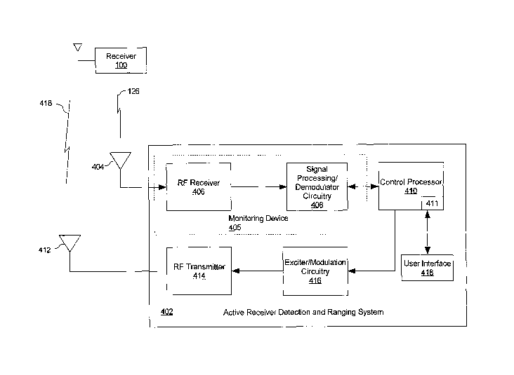
Turning now to FIG. 4, there is shown a block diagram of an active
receiver detection and ranging system (ARDRS) 402 that is useful for
understanding
the invention. The system includes an antenna 404 for acquisition of RF energy
associated with RF emissions 126 from a radio receiver 100. For example, the
antenna 404 can include a directional antenna system capable of focusing
antenna
gain in a selected direction. The RF energy from antenna 404 is communicated
to a
monitoring device 405, which includes RF receiver 406 and signal
processing/demodulator 408.
The RF receiver 406 can be a conventional design that is capable of
receiving RF emissions 126. Those skilled in the art will appreciate that it
can be
desirable to obtain information concerning one or more different types of RF
receivers
100. Accordingly, the RF receiver 100 can have a tuning range that covers RF
emissions known to be associated with the various different types of RF
receivers
100.
According to an embodiment of the invention, the RF receiver 406 has
a relatively narrow receiver bandwidth that is capable of being tuned to one
or more
frequencies associated with known RF emissions 126. Alternatively, the
receiver 406
can be a design that offers a bandwidth that is considerably larger. With a
wider
bandwidth design, the receiver 406 can provide the capability to concurrently
receive
one or more RF emissions 126 at various different RF frequencies. These RF
emissions 126 can be an LO signal and/or other RF emissions, such as harmonics
of
the LO and/or mixing products, all of which originate from a common receiver
100.
-10-
CA 02662562 2009-03-04
WO 2008/036582 PCT/US2007/078609
Depending on the design of RF receiver 406, signal
processing/demodulator circuitry 408 can be designed to process an RF emission
on a
single RF frequency or concurrently process a plurality of RF emissions
existing on
multiple RF frequencies. The signal processing/demodulator circuitry 408 also
includes at least one demodulator. The demodulator is advantageously selected
to be
of a type that is capable of providing a demodulated output in the form of a
signal
which is a representation of a variation associated with the RF emission 126.
For
example, a frequency modulation (FM) discriminator circuit could be used for
this
purpose. FM discriminator circuits are well known in the art and therefore
will not be
discussed here in detail. Similarly, an AM demodulator can be used to detect
variations in the amplitude of the RF emissions 126. Similarly, a phase
modulation
(PM) demodulator can be used to detect variations in the phase of the RF
emissions
126. Similarly, a demodulator may be advantageously devised to demodulate any
combination or one or more of these modulation formats simultaneously.
The ARDRS 402 also includes a transmitter antenna 412 coupled to an
RF transmitter 414. Those skilled in the art will appreciate that RF
transmitter 414
may in some cases be able to share a common antenna with RF receiver 406. For
example, a single antenna can be used if such antenna will provide acceptable
performance for receiving and transmitting signals as hereinafter described.
In that
case, a single antenna can be used in place of antennas 404 and 412, provided
that
appropriate isolation and diplexing or switching circuitry is provided to
isolate RF
receiver 406 from high power signals originating with the RF transmitter 414.
Still,
since a location of a receiver 100 may be unknown, it can be desirable in some
instances for a receiver antenna 404 to have a different antenna gain pattern
as
compared to the antenna gain pattern of a transmit antenna 412. In such cases,
it can
be more advantageous to use separate antennas 404, 412.
The RF transmitter is a conventional design capable of transmitting RF
signals on one or more frequencies that can be received by the RF receiver
100. It
should be understood that RF receiver 100 can be of one or more different
types. As
such, different RF receivers 100 can have different operating frequency
ranges.
-11-
CA 02662562 2009-03-04
WO 2008/036582 PCT/US2007/078609
Accordingly, the transmitter 414 is advantageously designed to provide a
transmit
frequency range which includes frequencies at which one or more RF receivers
100
can receive signals. The RF transmitter 414 is excited by exciter/modulation
circuitry
416. The exciter/modulation circuitry 416 can include an RF signal generator.
The
signal generator can include a phase locked loop (PLL) type RF generator to
provide a
stable source of RF energy for the RF transmitter. The PLL is preferably
designed to
produce RF energy at a selectable frequency within the range of the RF
transmitter
414.
The exciter/demodulation circuitry 416 can also include a modulation
circuit. The modulation circuit can include one or more of a phase modulator,
a
frequency modulator, an amplitude modulator, a modulator matching the type of
signal normally received by the Receiver 100, and a modulator advantageously
designed to maximize the variations in the emission or emissions. If multiple
types of
modulators are used, suitable control circuitry can be provided for
selectively
operating one or more modulators. Those skilled in the art will appreciate
that the
capability to simultaneously separately amplitude modulate and phase modulate
a
signal can reproduce any and all types of modulation. The exciter/modulation
circuitry 416, RF transmitter 414 and antenna 412 as described herein are
generally
known in the art and therefore will not be described in great detail.
The ARDRS 402 also includes a control processor 410. Control
processor 410 can be an ASIC, a microprocessor, a state machine, or a general
purpose computer which has been programmed with a suitable set of instructions
for
implementing the methods described herein. The control processor includes one
or
more devices suitable for storing a set of program instructions and/or data.
For
example, a data store 411 can be provided for this purpose. Data store 411 can
include RAM, ROM, and a bulk data storage device, such as a magnetic disc
drive.
The data store 411 is operatively connected to the control processor 410 by
conventional means such as data busses and or control circuits (not shown).
Note that
although the preferred embodiment of the invention incorporates a control
processor,
the use of a control processor is not necessary to implement the basic
functionality of
-12-
CA 02662562 2009-03-04
WO 2008/036582 PCT/US2007/078609
the invention -to detect a receiver. Purpose-made or general purpose
components
may be assembled to provide the basic detection mechanism with no explicit
control
processing.
The control processor 410 communicates with one or more of the
components of the ARDRS 402 by means of a suitable data bus or control lines.
For
example, the control processor 410 can receive demodulated signals from the
signal
processing/demodulator circuitry 408. It can also communicate command and
control
signals to control the monitoring device 405. Such signals can be used to
control any
functions performed by the RF receiver 406 and signal processing/demodulator
circuitry 408. The control processor 410 also advantageously provides control
signals
to the exciter/modulation circuitry 416 to control the output of RF
transmitter 414. In
general, the control processor 410 controls the operation of the monitoring
device
405, RF transmitter 414, and the exciter/modulation circuitry 416. A plurality
of
monitoring devices 405 can be used to detect signals at different frequencies
or
different sub-bands of frequencies, different modulation types, or any
combination of
these.
The control processor 410 also communicates with a user interface
418. The user interface 418 can communicate information to a user regarding
any RF
receiver 100 detected by the ARDRS 402. For example, the user interface 418
can be
used to identify a distance or range to the receiver 100, whether or not a
receiver 100
is receiving a signal from the ARDRS 402, and the minimum transmit power
necessary for signals to be received by RF receiver 100. The user interface
418 can
also provide means for a user to communicate input commands to control the
operation of the ARDRS 402 as hereinafter described.
The system described in FIG. 4 can be useful for implementing an
active receiver detection and ranging system in accordance with the invention.
Referring now to FIGS. 5A and 513, there is shown a process 500 that is useful
for
understanding the method for obtaining information regarding an RF receiver
100.
The method begins in step 502 with monitoring an RF emission 126 of an RF
receiver
100. For example, this step can be performed by monitoring device 405
operating in
-13-
CA 02662562 2009-03-04
WO 2008/036582 PCT/US2007/078609
conjunction with the control processor 410. In order to perform this step, it
is
preferred to have some preexisting knowledge as to the likely frequency of the
RF
emission 126. This information can be obtained as a result of industry
knowledge,
forensic investigation, or intelligence gathering activities. If an RF
emission 126 is
detected, it can be assumed that an RF receiver 100 of a predetermined type is
present. The information regarding the type of RF receiver 100 that has been
detected
can thereafter be used in step 504. Alternatively, if an RF emission is not
detected,
the process can continue as described below under the assumption that an RF
receiver
100 may be present in the area.
In step 504, the control processor 410 can cause exciter/modulation
circuitry 416, RF transmitter 414 and antenna 412 to generate an RF signa1418
on an
RF frequency that can be detected by the RF receiver 100. The details of this
RF
signal will be discussed in greater detail below. However, it should be
understood
that the RF signa1418 will cause a perturbation or variation in the RF
emission 126 if
it is received by the receiver 100. For example, each time the RF signa1418 is
received by the receiver 100, it will cause a slight shift in the frequency,
phase, and/or
amplitude of the LO 112 and the harmonics of such LO. This behavior is called
local
oscillator modulation or LOM.
In particular, an amplitude modulated RF signa1418 that is modulated
by a square wave waveform will cause power supply voltage variations in the
circuitry of the receiver 100. These variations may be due to overdrive of RF
and IF
circuits, normal current draw variations from the receiver 100's demodulation
circuitry 118 that correspond to the modulation input, normal current draw
variations
in the output driver circuits 120 as it reproduces the waveform, or other
causes. There
can also be other mechanisms that cause amplitude, phase, and/or frequency
modulations depending on the particular design of the receiver. Furthermore,
because
mixers and oscillators are inherently non-linear, emissions at twice, three
times, and
so on, the frequency of the local oscillator (its second, third, etc.
harmonics) can be
generated and radiated, all synchronized with the modulation of the RF
signa1418.
FIG. 3 illustrates the second harmonic of the LO, LO HARM 309. Of course, the
-14-
CA 02662562 2009-03-04
WO 2008/036582 PCT/US2007/078609
invention is not limited to a square wave amplitude modulation format. Any
other
waveform can be used that will cause modulation of the receiver's local
oscillator, its
harmonics, and mixing products. Use of a wide bandwidth modulation signal
(such
as a frequency chirp, square wave, or random or pseudorandom modulation) may
be
preferred since this can result in a wider bandwidth emission, that can be
more easily
detected due to the inherent processing gain advantage for a given detection
time
when using a filter matched to the modulation pattern.
A similar effect will occur with regard to other emissions, such as
mixing products. When the RF signa1418 is processed in mixer 110, it will
produce
various mixing products, including a Sum signa1308. The amplitude of the Sum
signa1308 and other mixing products will vary within some predetermined range
in
response to variations in the amplitude of the RF signa1418. In fact, any RF
signal
418 within the receive bandwidth of receiver 100 can be transmitted to the
receiver
100 and can be re-emitted at the Sum frequency 306. The limitation on such
amplitude variations can correspond to the point at which the front end
circuitry of
receiver 100 becomes saturated. If the RF signa1418 is a particular waveform,
the
waveform is detectable in the Sum signa1308 and any other harmonics of the Sum
signal. In any case, it will be appreciated that in this way the RF signa1418
can be
used to modulate the amplitude, phase, and/or frequency of the RF emission
126.
It has been found that the Sum 308 signal is particularly useful as an
RF emission 126. The usefulness of this particular signal arises from the fact
that it is
often spaced further apart in frequency from the RF signa1306 as compared to
the
frequency of the LO signa1304. Having the received signal 126 be significantly
different from the RF signa1418 in frequency can simplify the design of
circuitry
necessary to isolate the monitoring device 405 from high power output of the
RF
transmitter 414. For example, the filtering requirements for RF receiver 406
can be
less demanding because the Sum signa1308 or LO HARM signa1309 is further away
in frequency from the RF signa1418 which generally corresponds to RF frequency
306.
-15-
CA 02662562 2009-03-04
WO 2008/036582 PCT/US2007/078609
The amplitude, phase, and/or frequency shift in RF emission 126 can
be detected. It should be understood that as used herein, the term "RF
emissions"
include one or more of the LO signa1304, LO harmonics e.g. 309, mixing
products
including Sum 308, and various harmonics of these signals which radiate from
RF
receiver 100. Furthermore, "RF emissions" can include signals generated from
the
RF receiver using design considerations to transmit or re-radiate received
signals.
In step 506, a determination is made as to whether a variation or
perturbation has been detected in RF emission 126 in response to the RF
signa1418.
This determination can be performed by control processor 410. For example,
signal
processing/demodulator circuitry 408 can communicate a signal to control
processor
410 which indicates a variation has occurred in a frequency of RF emission
126. If
the control processor 410 determines that such a variation has occurred in
response to
a transmitted RF signa1418, then this serves as an indication that the RF
receiver 100
is receiving the RF signa1418 transmitted from the ARDRS 402. Consequently,
the
process can continue on to step 507.
In step 507, the control processor 410 can determine an amount of time
that has elapsed between the time that the RF signa1418 is generated in step
504 and
the time when a variation in the RF emission 126 corresponding to RF signa1418
was
detected by the monitoring device 405. This timing data is stored in a memory
location such as data store 411. Thereafter, the process continues on to step
508. The
purpose of the timing data will be described in more detail below.
In step 508, a determination is made by control processor 410 as to
whether the analysis of receiver 100 will include a determination of the
minimum
transmitter RF output power necessary for receiver 100 to receive signals from
ARDRS 402. If the analysis does include a determination of the minimum
required
transmitter RF output power, then the process proceeds to step 602. In step
602, the
control processor stores in a memory location of a data store a value
representative of
the current RF output power setting for the RF transmitter 414. For example,
the
value initially stored can be the maximum transmitter RF output power. In step
604,
the control processor reduces the RF output power from RF transmitter 414 by
some
-16-
CA 02662562 2009-03-04
WO 2008/036582 PCT/US2007/078609
predetermined amount. For example, the RF output power can be reduced by 1 dB,
2
dB, or 3dB. This reduction in RF output power can be accomplished by any one
of
several ways. For example, the RF output power from the exciter/modulation
circuitry 416 can be reduced by some predetermined amount, which will reduce
the
RF output power from the RF transmitter 414.
Following the adjustment to reduce the RF output power in step 604,
the method can continue on to step 606. In step 606, the control processor 410
can
control the exciter/modulation circuitry 416 and/or RF transmitter 414 to
cause them
to transmit an RF signa1418 on an RF frequency that can be received by the RF
receiver 100. The RF signal is transmitted at the power level established in
step 604.
The control processor 410 can then determine in step 610 whether the RF
signa1418
has caused a variation in the RF emission 126. The variation will coincide
with the
presence of the RF signa1418. If such a variation is detected, then that can
be
understood as an indication that the RF signa1418 was of sufficient power to
cause
the receiver 100 to receive the RF signa1418. Accordingly, the process returns
to step
602 and records the current RF output power value. Thereafter, steps 604
through
608 are repeated at progressively lower RF output power levels until little or
no
variation in RF emission 126 is detected in step 610.
When no variation is detected in step 610, this can be understood to
mean that the current RF output power level is too low to be received by
receiver 100.
The process then continues on to step 612 in which the system records that the
RF
output power value stored in the data store in step 602 is used to calculate
the lowest
RF output power level that can be used for establishing a communication link
from
the ARDRS 402 to the receiver 100. Once this value has been determined, the
process can continue to step 614 in which the RF output power level is reset.
This
step can involve setting the RF output power level to the minimum required RF
power
level for communicating with the receiver 100, as determined in steps 602
through
612. Alternatively, this step can involve setting the RF output power level
back to the
maximum power output. Of course, some intermediate value between these two
-17-
CA 02662562 2009-03-04
WO 2008/036582 PCT/US2007/078609
extremes could also be selected, or a control loop can be implemented to
enable
continuous determination of the required power level.
Following step 614, the process continues on to step 510. Similarly, if
it is determined in step 508 that there is no need to determine a minimum
required
power in step 508, then process can proceed directly to step 510 without
executing
steps 602 through 614. In step 510, a determination is made as to whether the
analysis of the receiver 100 should include a range determination. The range
determination is a process for determining a distance from the ARDRS 402 to
the
receiver 100. If such an analysis is to be performed, then the process
continues to step
516. In step 516, the control processor 410 can retrieve the timing data
(discussed in
step 507) from data store 411. Thereafter, the process continues on to step
518 in
which the control processor 410 calculates a distance between the ARDRS 402
and
the receiver 100. The timing data represents the time required for RF
signa1418 to
travel from ARDRS 402 to the RF receiver 100, cause a variation in RF emission
126,
and for RF emission 126 to travel from receiver 100 to the ARDRS 402. Those
skilled in the art will appreciate that this timing data, combined with the
well known
velocity of radio waves in free space, and any known signal processing delays
associated with the monitoring device 402 and propagation delays through the
RF
receiver 100, is sufficient information to calculate a distance between the
ARDRS 402
and the RF receiver 100.
Once this range or distance has been calculated in step 518, the process
continues to step 512. In step 512, the control processor 410 advantageously
generates an output notification to a user to indicate that a receiver 100 has
been
detected. The output notification can optionally include the minimum RF power
required to communicate RF signals to the receiver 100, and the range to the
receiver
100. Further, if the system described herein is combined with a directional
antenna
array or two or more antennas, then the output notification to the user can
also include
a bearing to the receiver 100.
In step 514, the control processor 410 can determine whether the active
receiver detection process is complete. Completion of the process can depend,
for
-18-
CA 02662562 2009-03-04
WO 2008/036582 PCT/US2007/078609
example, on a user input from user interface 418 terminating the process. If
the active
receiver detection process is complete then the process terminates. Otherwise,
the
process can return to step 502. Repeating the process can be advantageous for
increasing the accuracy of the range measurement described above. For example,
the
repetition of the range measurement process can be used to gather additional
data for
interpolation (dithering) of signals. By incrementing the frequencies (from a
list or
range of specified frequencies) of the monitor 405 and the transmitter 414
tuning
frequencies at this point and restarting at Step 502, a scan of a frequency
band or
bands may be effected for the case when the exact channel or frequency on
which the
receiver 100 is tuned is unknown.
It should be understood that the RF signa1418 can take a variety of
different forms, all of which are intended to be included within the scope of
the
present invention. For example, the RF signa1418 can have any combination of
amplitude, phase, or frequency modulation in accordance with a bit sequence.
This
bit sequence can define a predetermined modulation pattern. This predetermined
modulation pattern will cause the variation in RF emission 126 to occur in
accordance
with the modulation pattern. For example, if the RF signa1418 is amplitude
modulated so that it is turned on and off in accordance with a sequence of
data bits,
then the RF emission 126 can be expected to vary in phase, frequency, or
amplitude
each time the RF signa1418 is turned on or off. The frequency of the RF
emission
126 will therefore be modulated in accordance with the bit pattern in a manner
which
is similar to frequency shift keying (FSK), phase shift keying (PSK),
amplitude shift
keying (ASK), or any combination of amplitude and phase modulation.
The predetermined modulation pattern can be any sequence of data
bits. According to one embodiment of the invention, the control processor 410
can
generate a pseudo-random sequence of data bits that is based directly or
indirectly on
a pseudorandom number provided by an algorithm. Techniques for generating
pseudo random numbers are well known in the art.
Alternatively, or in addition to such pseudo random techniques, the RF
signa1418 can vary somewhat in frequency during the time it is transmitted.
For
-19-
CA 02662562 2009-03-04
WO 2008/036582 PCT/US2007/078609
example, the signal can be transmitted in the form of a chirp which increases
or
decreases in frequency over some period of time. For example, each pulse of
transmitted RF energy can be chirped in this way. The variation in the
frequency of
the RF signa1418 can cause a further variation in the frequency of the RF
emission
126. Of course, the invention is not limited in this regard, and any suitable
signal
format can be used for RF signa1418.
The selection of said modulation pattern to include a sequence of data
bits can be convenient for permitting the control processor to determine that
the
variation in RF emission 126 is the result of the RF signa1418, and not some
other
unanticipated effect. However, using a sequence of data bits in this way has
other
advantages as well. For example, the sequence of data bits can be used to
provide
additional processing gain that is useful for recovering weak RF emissions 126
from a
noisy RF environment. Conventional techniques, such as convolution processing
or
correlation, can be used to perform such processing and thereby aid in the
detection of
any variations that occur in the RF emissions 126. Such processing techniques
are
well known in the art and therefore will not be described here in detail.
However, it
should be understood that any suitable signal processing technique can be used
to
provide additional signal processing gain as would be understood by one
skilled in the
art.
-20-