Note : Les descriptions sont présentées dans la langue officielle dans laquelle elles ont été soumises.
CA 02713153 2010-07-23
WO 2009/111187
PCT/US2009/034749
INTEGRATED CIRCUIT WITH MOSFET FUSE ELEMENT
FIELD OF THE INVENTION
This invention relates generally to integrated circuits, and more particularly
to
programming a one-time-programmable logic memory cell having a metal-oxide-
semiconductor ("MOS") fuse.
BACKGROUND OF THE INVENTION
Many integrated circuits ("ICs") are made up of millions of interconnected
devices, such as transistors, resistors, capacitors, and diodes, on a single
chip of
semiconductor substrate. It is generally desirable that ICs operate as fast as
possible, and consume as little power as possible. Semiconductor ICs often
include one or more types of memory, such as CMOS memory, antifuse
memory, and efuse memory.
One-time-programmable ("OTP") memory elements are used in ICs to provide
non-volatile memory ("NVM"). Data in NVM are not lost when the IC is turned
off. NVM allows an IC manufacturer to store lot number and security data on
the IC, for example, and is useful in many other applications. One type of NVM
is commonly called an E-fuse.
E-fuses are usually integrated into semiconductor ICs by using a stripe
(commonly also called a "link") of conducting material (metal, poly-silicon,
etc.)
between two pads, generally referred to as anode and cathode. Applying a fuse
current (IFusE) to the E-fuse destroys the link, thus changing the resistance
of the
E-fuse. This is commonly referred to as "programming" the E-fuse. The fuse
state (i.e., whether it has been programmed) can be read using a sense
circuit,
which is common in the art of electronic memories.
Fig. 1 is a plan view of an E-fuse 100. The E-fuse 100 has a fuse link 102
between an anode 104 and a cathode 106. The anode, fuse link, and cathode
are typically polysilicon or silicided polysilicon formed entirely on
relatively thick
field oxide or isolation oxide. Contacts (not shown) provide electrical
terminals to
the anode and cathode. The fuse link has a relatively small cross section,
which
results in Joule heating of the link during programming to convert the E-fuse
to a
high resistance state. The terms "anode" and "cathode" are used for purposes
of convenient discussion. Whether a terminal of an E-fuse operates as an anode
or a cathode depends upon how the programming current is applied.
1
CA 02713153 2010-07-23
WO 2009/111187
PCT/US2009/034749
Programming of the E-fuse can be facilitated by the physical layout. For
example, the cathode 106 is larger than the fuse link 102, which generates
localized Joule heating in the fuse link during programming.
During programming, a controlled level of current flows through the fuse link
for a
specified period. The programming current heats up the fuse link more than the
adjacent areas due to current crowding and differences in heat dissipation,
creating a temperature gradient. The temperature gradient and the carrier flux
causes electro- and stress-migration to take place and drive material (e.g.,
silicide, dopant, and polysilicon) away from the fuse link.
Programming generally converts the E-fuse from an original resistance to a
programmed resistance. It is desirable for the programmed resistance to be
much higher (typically many orders of magnitude higher) than the original
resistance to allow reliable reading of the E-fuse using a sensing circuit. A
first
logic state (e.g., a logical "0") is typically assigned to an unprogrammed,
low-
resistance (typically about 200 Ohms) fuse state, and a second logic state
(e.g.,
a logical "1") to the programmed, high-resistance (typically greater than
100,000
Ohms) fuse state. The change in resistance is sensed (read) by a sensing
circuit to produce a data bit.
E-fuse elements are particularly useful due to their simplicity, low
manufacturing
cost, and easy integration into CMOS ICs using conventional CMOS fabrication
techniques. However, undesirable problems such as uncontrolled programming
(i.e., overprogramming or underprogramming) or physical damage to adjacent
structures can occur, resulting in leakage currents in nearby FETs. Other
problems arise when ICs are scaled to smaller design geometries (node
spacings) because the programming conditions for one design geometry might
not be optimal for another design geometry, undesirably reducing programming
yield or increasing programming time. It is desirable to provide E-fuse
techniques that overcome the problems of the prior art.
SUMMARY OF THE INVENTION
At least one MOS parameter of a MOS fuse is characterized to provide at least
one reference MOS parameter value. Then, the MOS fuse is programmed by
applying a programming signal to the fuse terminals so that programming
current
flows through the fuse link. The fuse resistance is measured to provide a
2
CA 02713153 2010-07-23
WO 2009/111187
PCT/US2009/034749
measured fuse resistance associated with a first logic value. A MOS parameter
of the programmed MOS fuse is measured to provide a measured MOS
parameter value. The measured MOS parameter value is compared to the
reference MOS parameter value to determine a second logic value of the MOS
fuse, and a bit value is output based on the comparison.
BRIEF DESCRIPTION OF THE DRAWINGS
Fig. 1 is a plan view of a prior art E-fuse.
Fig. 2A is a plan view of a MOS fuse according to an embodiment
Fig. 2B is a cross section of the MOS fuse of Fig. 2A taken along section line
A-
A.
Fig. 2C is a cross section of the MOS fuse of Fig. 2A taken along section line
B-
B.
FIG. 3 is a symbol of a MOS fuse according to an embodiment.
Fig. 4 is a diagram of a sensing circuit for sensing the logic state of a MOS
fuse
according to an embodiment.
FIG. 5 is a flow chart of a method of operating a MOS fuse according to an
embodiment.
FIG. 6 is a plan view of an FPGA according to an embodiment.
DETAILED DESCRIPTION OF THE DRAWINGS
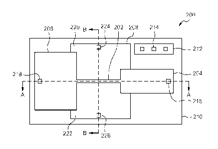
Fig. 2A is a plan view of a MOS fuse 200 according to an embodiment. The
MOS fuse 200 includes a fuse link 202 extending between an anode 204 and a
cathode 206. The fuse link 202 extends across an active region 208 of
semiconductor material (e.g., silicon), unlike conventional E-fuses that are
defined on thick oxide.
In a particular embodiment, the anode, cathode, and fuse link are silicided
polysilicon, and the fuse link is separated from the active region of the
semiconductor material by a thin oxide layer, which in a particular embodiment
is
a gate oxide layer, which is a thin oxide layer formed over active silicon
(e.g., a
channel region of a MOSFET). In a particular embodiment, the thin oxide layer
is less than 50 nm thick, and in a further embodiment is a gate oxide layer
not
more than 10 nm thick. In some embodiments, portions of the anode and
cathode also overlie the active region, and are separated from the active
region
3
CA 02713153 2010-07-23
WO 2009/111187
PCT/US2009/034749
of semiconductor material by the thin oxide layer. Polysilicon deposition,
photolithography, and silicidation are commonly used in conventional CMOS
fabrication techniques to define gate structures of FETs, and embodiments of
the
invention are easily incorporated into CMOS ICs using standard processing. For
purposes of convenient discussion, the anode-link-cathode structure will be
referred to as a "fuse element", which will be used to describe this feature
both
before programming and after programming, when the fuse link is likely
substantially gone, and the term "fuse resistance" will be used for purposes
of
discussion to indicate the resistance of (through) the fuse element.
The active region 208 is formed in a well 210 formed in a semiconductor
substrate, such as a silicon wafer. A well tap 212 provides an electrical
connection to the well 210 through contacts 214, which allow the well to be
biased at a selected potential or allow detection of well potential or
current.
Contacts 216, 218 similarly provide electrical connections to the anode 204
and
cathode 206 for programming the fuse link and sensing the logic state of the
fuse
link.
Source/drain ("SID") regions 220, 222 are also formed in the active region
208.
SID diffusions (see Fig. 20, ref. nums. 221, 223) are formed in the SID
regions.
SID regions and diffusions are well known in the art of MOS FETs; however, the
fuse link 202 of the MOS fuse 200 operates very differently than the gate of a
MOS FET. While the MOS-fuse can be biased and operated in the same
manner as a MOSFET, in which case anode or cathode terminals can act as
gate (which may be tied together or only one of them may be biased), the fuse
link is intended to be programmed. The anode and cathode terminal allow
substantial direct current to flow through the fuse link 202 during
programming.
In a conventional MOSFET, direct current through the gate is generally
undesirable, and conventional gates are biased to a single, common potential,
and often have only a single gate terminal. Contacts 224, 226 provide
electrical
connections to the SID regions 220, 222.
In a particular embodiment, the anode 204, cathode 206, and fuse link 202 are
defined from a polysilicon layer deposited on the silicon wafer using
photolithographic techniques. Gate electrodes of FETs and other polysilicon
features are typically also defined from the polysilicon layer when the MOS
fuse
200 is incorporated in a CMOS IC. Optionally, a layer of silicide-forming
4
CA 02713153 2010-07-23
WO 2009/111187
PCT/US2009/034749
material, of which several are known, is deposited on the substrate and
processed to form silicide on exposed silicon. Silicide forms on the exposed
polysilicon of the anode, link, and cathode, and on the exposed silicon of the
S/D
regions 220, 222.
Fig. 2B is a cross section of the MOS fuse of Fig. 2A taken along section line
A-
A. The well 210 is formed in a silicon substrate 230. The well can be P-type
or
N-type, depending on how the MOS fuse is intended to be operated (biased).
The active area 208 underlies the fuse link 202 and portions 232, 234 of the
anode and cathode. Remaining portions of the anode and cathode (see Fig. 2A,
ref. nums. 204, 206 overlie thick oxide 236, which in a particular embodiment
is
formed from an oxide layer used in a shallow trench isolation application in
other
portions of a CMOS IC. A gate oxide layer 238 separates the polysil icon 240
of
the anode-link-cathode structure from the silicon in the active area 208. A
silicide layer 242 is shown above the remaining polysilicon layer 240, and is
formed by depositing a silicide-forming layer and reacting the silicide-
forming
material with a portion of the polysilicon layer. Alternatively, the
polysilicon is
entirely silicided, and there is no remaining polysilicon layer, or a silicide
layer is
deposited over polysilicon without consuming polysilicon.
Contacts 216, 218 electrically connect metal traces 244, 246 in a patterned
metal layer (commonly referred to as the "Ml layer") in an IC. The metal
traces
244, 246 are not shown in the plan view of Fig. 2A for clarity of illustration
of
underlying features. An oxide layer 248 is deposited on the substrate and
processed to provide holes for the contacts and a surface for the metal
traces,
as is known in the art. Similar techniques are used to connect FETs and other
devices in a CMOS IC. An IC typically has additional patterned metal layers
(M2, M3, etc., not shown) that are interconnected with vias, and provide
electrical connections from external pads to various internal nodes of the IC.
Fig. 2C is a cross section of the MOS fuse of Fig. 2A taken along section line
B-
B. Metal traces 250, 252 are connected to the SID regions 220, 222 through
contacts 224, 226 extending through oxide layer 248. The S/D regions have
been silicided 254, which is shown using a different reference numeral than
silicide 242 in the fuse link because the silicide is formed from silicon in
the
active region 208. The polysilicon 240 and gate oxide 238 between the fuse
link
and active region 208 are also shown. SID diffusions 221, 223 are formed in
the
5
CA 02713153 2010-07-23
WO 2009/111187
PCT/US2009/034749
substrate 230. Other features, such as lightly-doped drain ("LDD") are
optionally
formed. Optional sidewall spacers 260, 262 are formed on the sidewalls of the
fuse link polysilicon 240 prior to deposition of the silicide forming layer as
part of
a conventional CMOS process flow. They may be left on the sidewalls of the
fuse link (poly sidewalls) as shown, or removed.
The SID contacts 224, 226, and well contact (see Fig. 2A, ref. num. 214) in
cooperation with the other contacts of the MOS fuse, allow measurement of
additional MOS fuse characteristics, such as anode or cathode current leakage
to the active region 208, source-drain junction currents, or drain to source
channel current. The MOS fuse is characterized before programming, such as
by measuring the initial values of one or more selected parameters of the MOS
fuse or by determining characteristic values from wafer electrical test, and
the
measured MOS parameter(s) of the MOS fuse is compared against the
specification to determine whether the measured MOS parameter indicates a
programmed or unprogrammed state.
If the measured value(s) is essentially the same as the initial value(s), it
indicates
that the MOS fuse was not programmed. If the measured value(s) is
significantly
different from the initial value(s), it indicates that the MOS fuse was
programmed. If the fuse link was incompletely programmed, or if programming
of the fuse link caused physical damage that reduced the programmed
resistance between the anode and cathode, the programming of that bit is
invalid. In some cases, an improperly programmed bit might have an anode-
cathode resistance sufficiently low that it falls below the resistance
specification
for a programmed bit. The additional measured values of the MOS fuse provide
an indication as to the programming status (i.e., logic value) of the bit. The
additional MOS fuse information can be used to detect and alarm an improperly
programmed fuse, or can be used as a secondary indication of logic value
(i.e.,
in an OR operation with fuse link resistance) to improve overall programming
yield and programming reliability. For example, a MOS parameter(s) may be
used to detect and indicate an improper programming condition applied by en
end user, or to help identify optimized programming parameters.
FIG. 3 is a symbol 300 of a MOS fuse according to an embodiment. The MOS
fuse has five terminals: an anode 302, a cathode 304, a drain 306, a source
308
and a well tap 310. In some embodiments, the SID regions (see Fig. 2A, ref.
6
CA 02713153 2010-07-23
WO 2009/111187
PCT/US2009/034749
nunns. 220, 222) are substantially the same, and whether one of the SID
regions
operates as a source or as a drain depends upon bias conditions, as is known
in
the art of FETs. The fuse link 312 provides a low resistance (typically not
more
than about 200 Ohms) path between the anode 302 and cathode 304. After
programming, it is desirable that the resistance between the anode and cathode
is much greater, in some cases at least 10,000 Ohms. Bits (fuse links) with
lower after-programming resistance are often referred to as "tail bits," and
are
often not used, their data being programmed into redundant bits. It is
generally
desirable to reduce the number of tail bits in a programmed fuse array. Gate
oxide thickness is preferably thick enough so that proper programming
conditions (i.e., controlled fuse link blowing) does not substantially
increase
leakage. For purposes of convenient discussion, the S, D, and B terminals of
the MOS fuse 300 will be referred to as "MOS terminals" and the A and C
terminals will be referred to as "fuse terminals".
Fig. 4 is a diagram of a sensing circuit 400 for sensing the logic state of a
MOS
fuse 300 according to an embodiment. During programming, Read_A and
Read_B are disabled. A high voltage (typically about 3 to 4 Volts) is applied
to
Vfs and M1 is turned on for a selected period commonly called a programming
pulse Pgm, which in a particular embodiment is about 100 to 1000 micro
seconds. The Pgm pulse allows programming current to flow from Vfs to the
anode, through the fuse link, to the cathode, and through M1 to ground. Sense
Block B is disabled during programming, and the MOS terminals S, B, D of the
MOS fuse 300 are floating.
For a READ operation, either a one-step or two-step READ is performed. If the
MOS fuse 300 has been verified to have suitably high anode-cathode resistance,
the Sense Block A is used to latch Dout_A by measuring the poly fuse link
resistance, as in a conventional E-fuse. Pgm is OFF and Vfs is switched to
ground or left floating. A Read _A signal turns on M2, which allows sensing
current lread to flow through M2, through the cathode-anode of the MOS fuse
300, and through M3 to ground. If the fuse resistance is high (i.e., the fuse
link
has been successfully programmed), the programmed bit causes the Sense
Block A input (from !read) to be higher than if the bit was unprogrammed
(i.e., if
the fuse resistance was in a low, unprogrammed value (also referred to as
pristine or as-fabricated fuse resistance). The Sense Block A detects whether
7
CA 02713153 2010-07-23
WO 2009/111187
PCT/US2009/034749
the input value indicates high or low fuse resistance, and produces the
corresponding digital logic output value Dout_A.
The MOS fuse programming state (stored digital logic value) can also be read
(sensed) using the MOS terminals S, B, D along with corresponding bias
condition for C and A. Read_A is disabled, and Vfs is floated, and Read_B is
asserted to activate Sense Block B. Sense Block B measures one or several
MOS fuse parameters, such as fuse element-to-active silicon leakage current,
source-to-well leakage, drain-to-well leakage current, source-to-drain leakage
current (with C and A grounded), drain-to source channel on-current (with C
and
A biased), and compares the measured value(s) with stored initial values
(e.g.,
measured values of the unprogrammed (pristine) MOS fuse or characteristic or
expected pristine values). If the READ measured value(s) is within the
expected
range for the unprogrammed MOS fuse, a first logical data value (e.g., a data
"0") is generated and latched at Dout_B. If the READ measured value indicates
that the MOS fuse has been programmed (i.e., a sufficient change in one or
more MOS fuse parameters measured at the one or more MOS terminals S, B,
D has occurred), a second logical data value (e.g., a data "1") is generated
and
latched at Dout_B.
The first or second READ techniques can be used alone in a READ operation, or
both can be used in a dual-READ operation. In other words, the first READ
technique is used to sense the fuse resistance, and a second READ technique is
used to sense the programming state (stored digital logic value) of the MOS
fuse
using the MOS terminals S, B, D. The Dout_A value is compared to the Dout_ B
value at a Bit Data Comparator. In a particular embodiment, if either Dout_A
or
Dout_B indicates that the MOS fuse 300 has been programmed, the Bit Data
Comparator generates a digital logic value (e.g., digital "1") corresponding
to a
programmed bit. In other words, the single MOS fuse 300 has redundant
storage.
In a further embodiment, the Bit Data Comparator generates a Sense_flag
output if Dout_A is a different digital data value than Dout_B. For example,
if a
MOS fuse programming step fails to provide a sufficiently high fuse resistance
to
set Dout_A to a programmed value, but sensing the MOS terminals indicates
that a programming step had been applied to the MOS fuse, then the Sense_flag
would be asserted to indicate a discrepant programming step; however, the
logic
8
CA 02713153 2010-07-23
WO 2009/111187
PCT/US2009/034749
state of the MOS fuse would still be correctly indicated by Dout_B and the OR
operation provided by the Bit Data Comparator. This reduces the number of fail
bits, and also provides an indication of the efficiency of the programming
operation. In other embodiments, other logic gates or functions, such as an
AND
operation, may be used in the Bit Data Comparator.
FIG. 5 is a flow chart of a method 500 of operating a MOS fuse according to an
embodiment. A MOS fuse having fuse terminals and MOS terminals is provided
(step 502). At least one MOS parameter is characterized before programming
(step 504). In a particular embodiment, one or more MOS parameters of the
MOS fuse are measured, and the initial MOS parameter values are stored for
future comparison. Examples of MOS parameters include fuse element-to-active
silicon leakage current, source-to-well leakage, drain-to-well leakage
current,
source-to-drain leakage current, drain-to-source, and channel ON current. The
MOS fuse is programmed (step 506) by applying a programming signal through
the fuse terminals. Generally, the programming signal is a selected amount of
current applied through the fuse element for a selected period of time
sufficient
to significantly increase the resistance between the fuse terminals after
programming, typically by fusing the fuse link. In a particular embodiment,
the
programming signal is a three to four volt signal applied for about 0.1msec to
about 10 ms to a fuse element having an initial (as-fabricated) resistance of
about 200 Ohms. After programming, the fuse element is desired to have a
programmed resistance of at least 10,000 Ohms.
After programming, the resistance between the fuse terminals is measured (step
508) and compared against a fuse resistance reference value to determine a
first
digital logic value (step 510) of the MOS fuse, i.e., to determine whether the
fuse
resistance indicates that the MOS fuse has been programmed. After
programming, one or more MOS parameters of the MOS fuse are measured to
provide at least one measured MOS parameter value (step 512), and the
measured value(s) is compared against the MOS parameter reference value(s)
to determine a second digital logic value (step 514) of the MOS fuse. It is
generally expected that the first and second digital logic values are the same
value (i.e., both are 0 or both are 1); however, in some cases the first
digital logic
value might be different than the second digital logic value. Alternatively,
the
MOS parameter(s) is read before the fuse resistance.
9
CA 02713153 2010-07-23
WO 2009/111187
PCT/US2009/034749
The first digital logic value is compared to the second digital logic value
(step
516). If either the first digital logic value or the second digital logic
value is
consistent with a programmed value (i.e., if either the fuse resistance or MOS
parameter(s) indicate that the MOS fuse was subjected to a programming pulse),
a programmed bit value (see Fig. 4, Dout) is output (step 518). In a further
embodiment, if the first digital logic value is different than the second
digital logic
value, a sense flag is output (step 520), indicating that the fuse element
might
have been improperly programmed. In a particular embodiment, the sense flag
is enabled if the first digital logic value is an invalid programmed value and
the
second digital logic value is a valid programmed value.
FIG. 6 is a plan view of a field programmable gate array (FPGA) according to
an
embodiment. The FPGA includes CMOS portions in several of the functional
blocks, such as in RAM and logic, and is fabricated using a CMOS fabrication
process. MOS fuses programmed according to one or more embodiments of the
invention are incorporated in any of several functional blocks of the IC, such
as a
memory block, logic block, I/O block, clock circuit, transceiver, or other
functional
block; within many functional blocks; or within a physical section or segment
of
the FPGA 600. MOS fuses programmed according to one or more embodiments
of the invention are particularly desirable for non-reconfigurable, NV memory
applications, such as serial numbers, storing security bits that disable
selected
internal functions of the FPGA, bit-stream encryption key storage, or to
provide a
user general-purpose one-time programmable NV user-defined bit storage.
The FPGA architecture includes a large number of different programmable tiles
including multi-gigabit transceivers (MGTs 601), configurable logic blocks
(CLBs
602), random access memory blocks (BRAMs 603), input/output blocks (I0Bs
604), configuration and clocking logic (CONFIG/CLOCKS 605), digital signal
processing blocks (DSPs 606), specialized input/output blocks (I/O 607) (e.g.,
configuration ports and clock ports), and other programmable logic 608 such as
digital clock managers, analog-to-digital converters, system monitoring logic,
and
so forth. Some FPGAs also include dedicated processor blocks (PROC 610).
In some FPGAs, each programmable tile includes a programmable interconnect
element (INT 611) having standardized connections to and from a corresponding
interconnect element in each adjacent tile. Therefore, the programmable
interconnect elements taken together implement the programmable interconnect
CA 02713153 2010-07-23
WO 2009/111187
PCT/US2009/034749
structure for the illustrated FPGA. The programmable interconnect element (INT
611) also includes the connections to and from the programmable logic element
within the same tile, as shown by the examples included at the top of Fig. 6.
For example, a CLB 602 can include a configurable logic element (CLE 612) that
can be programmed to implement user logic plus a single programmable
interconnect element (INT 611). A BRAM 603 can include a BRAM logic
element (BRL 613) in addition to one or more programmable interconnect
elements. Typically, the number of interconnect elements included in a tile
depends on the height of the tile. In the pictured embodiment, a BRAM tile has
the same height as four CLBs, but other numbers (e.g., five) can also be used.
A DSP tile 606 can include a DSP logic element (DSPL 614) in addition to an
appropriate number of programmable interconnect elements. An 10B 604 can
include, for example, two instances of an input/output logic element (10L 615)
in
addition to one instance of the programmable interconnect element (INT 611).
As will be clear to those of skill in the art, the actual I/O pads connected,
for
example, to the I/O logic element 615 are manufactured using metal layered
above the various illustrated logic blocks, and typically are not confined to
the
area of the input/output logic element 615. In the pictured embodiment, a
columnar area near the center of the die (shown shaded in Fig. 6) is used for
configuration, clock, and other control logic.
Some FPGAs utilizing the architecture illustrated in Fig. 6 include additional
logic
blocks that disrupt the regular columnar structure making up a large part of
the
FPGA. The additional logic blocks can be programmable blocks and/or
dedicated logic. For example, the processor block PROC 610 shown in Fig. 6
spans several columns of CLBs and BRAMs.
Note that Fig. 6 is intended to illustrate only an exemplary FPGA
architecture.
The numbers of logic blocks in a column, the relative widths of the columns,
the
number and order of columns, the types of logic blocks included in the
columns,
the relative sizes of the logic blocks, and the interconnect/logic
implementations
included at the top of Fig. 6 are purely exemplary. For example, in an actual
FPGA more than one adjacent column of CLBs is typically included wherever the
CLBs appear, to facilitate the efficient implementation of user logic.
While the present invention has been described in connection with specific
embodiments, variations of these embodiments will be obvious to those of
11
CA 02713153 2013-05-29
ordinary skill in the art. For example, alternative layouts and cross-sections
of
MOS fuses could be alternatively used, and alternative sensing circuitry can
be
used.
In the foregoing specification, the invention has been described with
reference to
specific embodiments thereof. However, the scope of the claims should not be
limited by the preferred embodiments set forth in the examples, but should be
given the broadest interpretation consistent with the description as a whole.
The
specification and drawings are, accordingly, to be regarded in an illustrative
rather than a restrictive sense.
12