Note : Les descriptions sont présentées dans la langue officielle dans laquelle elles ont été soumises.
CA 02726167 2010-11-26
Description
Title of Invention: DRIVE CONTROL DEVICE FOR OSCILLATOR, DRIVE
CONTROL METHOD FOR OSCILLATOR, AND MANUFACTURING METHOD FOR
OSCILLATOR
Technical Field
[0001] The present invention relates to a drive control device
for an oscillator, a drive control method for an oscillator, and
a manufacturing method for an oscillator. An oscillator is generally
configured to obtain an oscillation by means of an electromagnetic
coil or a piezoelectric element, and the obtained oscillation needs
to be set to proper oscillation characteristics according to
applications, namely proper oscillation frequency and amplitude.
Moreover, the oscillation obtained in this way is used in various
devices for providing oscillations.
[0002] Those various devices include a part feeder for feeding
parts stored in a circular bowl, a vibratory hopper for supplying
the bowl of the part feeder with the parts by vibrating a part feeder
plate provided in a tilted manner to a part container in a rectangular
box shape, a linear feeder for linearly feeding parts, and a device
for grinding a part by oscillating a container containing a large
number of parts.
Background Art
[0003] Typical examples of the applications of the oscillator
1
CA 02726167 2010-11-26
as mentioned above include an electromagnetic vibratory part feeder
using oscillations generated by an electromagnetic coil, for example.
The part feeders of this kind include a part feeder provided with
a circular bowl in which a part-transport path in a spiral shape
is formed, and which stores parts such as projection nuts (refer
to Patent Literature 1, for example).
[ 0004 ] The circular bowl of the vibratory part feeder of this
kind has a part-transport path in a spiral shape formed along an
internal wall surface. An attracted portion fixed on a back surface
of a bottom portion of the bowl is supported by top ends of a plurality
of spring members, and bottom ends of the plurality of spring members
are fixed at a predetermined inclined angle to a base member in
a stationary state. An electromagnetic coil is provided on the base
member, and the attracted portion is intermittently attracted by
turning ON/OFF of power supply to the electromagnetic coil, thereby
imparting a composed oscillation in a circumferential direction
and a vertical direction to the bowl. As a result, a large number
of parts fed to the bottom portion of the bowl are sequentially
transported in an aligned state along the part-transport path, and
are fed out from a feed-out tube on a top end portion of the bowl.
[0005] The vibratory part feeder disclosed in Patent Literature
1 provides control of always maintaining a constant amplitude of
the part feeder within a drive circuit without providing a special
detector for detecting an oscillation state to a main unit of the
part feeder in response to a change in weight of the parts in the
2
CA 02726167 2010-11-26
bowl caused by the feed-out of the parts, or a slight variation
in power supply voltage caused by electric power used in a plant.
[0006] In other words, the vibratory part feeder is configured
to detect, by current detection means, a current flowing through
the electromagnetic coil, decompose, by higher harmonic analysis
means, the detected current into higher harmonic components, compare
and calculate, by oscillation calculation means, a high-order
current signal based on an oscillation of a mechanical system out
of the higher harmonic components and a set current signal set in
advance for generating a predetermined amplitude, and control a
drive current of a drive power supply according to the calculated
result so that a detected current value and a set current value
coincide with each other.
[0007] The vibratory part feeder disclosed in Patent Literature
1 uses the current, particularly, a correlation between the current
component of the higher harmonic based on the mechanical system
of the part feeder and the amplitude. Therefore, the entire
processing is carried out by the electronic circuit in a control
device without providing a special detector to the main unit of
the part feeder, thereby providing an appropriate feedback control
of the amplitude following a variation in the part weight or the
like.
Citation List
Patent Literature 1: JP 07-60187 A
3
CA 02726167 2010-11-26
Summary of Invention
Technical Problem
[0008] However, it is necessary for each vibratory part feeder
of this kind to be adjusted for generating a stable constant
oscillation in response not only to a change in weight of the parts
in the bowl caused by the feed-out of the parts, and a slight variation
in power supply voltage caused by electric power used in a plant
mentioned above, but also to changes in frequency and amplitude
of the power supply voltage which are different depending on a delivery
destination of the vibratory part feeder (location where the
vibratory part feeder is installed) which has unique frequency and
amplitude of the power supply.
[0009] If the constant oscillation cannot be maintained, the
number of fed parts per predetermined period varies, and normal
continuity to a subsequent electric resistance welding process and
the like cannot be secured, resulting in a trouble in a production
management.
[00101 As an AC power supply unique to the delivery destination
mentioned above, while an electric power supply having two types
of frequency, 50 Hz and 60 Hz, and two types of amplitude, 100 V
and 200 V, are used in Japan, for example, an electric power supply
having a frequency of 50 Hz and two types of amplitude, 115 V and
230 V is used in Europe or other part of the world, for example.
The actual condition is that the frequency and the amplitude of
4
CA 02726167 2010-11-26
the power supply used for driving the vibratory part feeder vary
depending on domestic and overseas delivery destinations as
described above.
[0011] As described above, those delivery destinations are
different in frequency and amplitude of the power supply, and hence
if the vibratory part feeder which has been adjusted upon the factory
delivery or the like is installed in the delivery destination, it
is necessary to readjust the frequency (oscillation frequency) and
the amplitude of the output voltage of a drive control device so
that a drive system of the vibratory part feeder is driven at a
stable and constant oscillation according to the unique power supply
voltage used at the delivery destination.
[0012] In response to a change in weight of the parts in the
bowl caused by the feed-out of the parts, or a slight variation
in power supply voltage caused by the electric power used in the
plant as mentioned above, the part feeder may be adjusted by using
the correlation between the current component of the higher harmonic
based on the mechanical system of the part feeder and the amplitude
as disclosed in Patent Literature 1. In other words, the frequency
and the amplitude of the output voltage of the drive control device
need to be finely adjusted in response to the change in weight of
the parts in the bowl, and the slight variation in power supply
voltage caused by the electric power used in the plant.
[0013] However, it is difficult to adapt to a situation of the
power supply voltage unique to the delivery destination of the
CA 02726167 2010-11-26
vibratory part feeder, which widely ranges from 100 V to 230 V,
for example, only by finely adjusting the frequency and the amplitude
of the output voltage of the drive control device as the vibratory
part feeder disclosed in Patent Literature 1, and it is necessary
to largely adjust the frequency and the amplitude of the output
voltage of the drive control device.
[0014] Moreover, if the adaptation is difficult to be achieved
only by adjusting the frequency and the amplitude of the output
voltage of the drive control device, the electromagnetic coil and
the spring members need to be replaced, but the replacement of the
electromagnetic coil and spring members requires experience and
time, which causes a decrease in work efficiency, resulting in
difficulty in quick adaptation.
[0015] The present invention is made in view of the
above-mentioned problems, and has an object of providing a drive
control device for an oscillator, a drive control method for an
oscillator, and a manufacturing method for an oscillator capable
of adapting to unique power supply voltages having different
frequencies and amplitudes so as to drive an oscillator always at
a stable and constant oscillation even if the frequency and the
amplitude of the power supply voltage differ depending on the delivery
destination of the oscillator and the range of change in the power
supply voltage in the delivery destination is wide.
[0016] Moreover, there are examples in which the oscillation
frequency of the vibratory part feeder is set to 50 times or 60
6
CA 02726167 2011-10-26
times per second based on the frequency of the commercial power
supply (50 Hz and 60 Hz in Japan) , which are not mentioned in Patent
Literature 1. However, if there are fixed two types of frequency,
it is impossible to flexibly adapt to changes in mass of an oscillating
portion (bowl) of the vibratory part feeder and parts. In other
words, the vibratory part feeder needs to have a specification proper
for 50 or 60 times of oscillations per second, and there thus poses
a problem of a decreased degree of freedom in terms of design.
Solution to Problem
[0017] As an aspect of the present invention to attain the
above-mentioned object, according toclaim lofthe present invention,
there is provided a drive control device for an oscillator, which
generates a predetermined switching pattern by operating a switching
element, and supplies an oscillation generation unit of an oscillator
with drive electric power for generating predetermined oscillation
frequency and amplitude according to the switching pattern, the
oscillator drive control device at least including: a voltage
detection circuit for detecting a power supply voltage unique to
a delivery destination of the oscillator; a memory circuit storing,
in advance, a basic switching pattern adapted to an arbitrarily
set reference voltage, and used for driving the oscillation
generation unit at proper oscillation frequency and amplitude; and
an arithmetic processing circuit for calculating a ratio of the
detected voltage unique to the delivery destination detected by
7
CA 02726167 2010-11-26
the voltage detection circuit to the reference voltage, and
calculating, based on the ratio, a switching pattern substantially
the same as the basic switching pattern under an environment of
the power supply voltage unique to the delivery destination. It
should be noted that "delivery destination" refers to a region in
which the oscillator is to be installed. It should be noted that
"power supply voltage unique to the delivery destination" refers
to power supply voltage unique to the plant in which the oscillator
is to be installed.
[0018] The drive control device for the oscillator according
to the present invention includes, as a main portion, the voltage
detection circuit, the memory circuit, and the arithmetic processing
circuit that are described above, and hence a constant oscillation
can always be generated by the oscillation generation unit of the
oscillator according to the power supply voltage having the amplitude
unique to the delivery destination at which the oscillator is to
be installed.
[0019] In other words, the power supply voltage unique to the
delivery destination at which the oscillator is to be installed
is detected by the voltage detection circuit, the ratio of the detected
voltage output from the voltage detection circuit to the reference
voltage set arbitrarily is calculated by the arithmetic processing
circuit, the basic switching pattern proper for the oscillator in
a case where the switching element is driven at the reference voltage
is read out from the memory circuit, and the switching pattern
8
CA 02726167 2010-11-26
substantially the same as the basic switching pattern under the
environment of the power supply voltage unique to the delivery
destination is calculated based on the ratio described above by
the arithmetic processing circuit.
[0020] Asa result, an output voltage of the drive control device
generated by a switching operation of the switching element is made
coincident with an output voltage in the case where the switching
element is driven at the reference voltage, even under the environment
of the power supply voltage at the delivery destination. In other
words, the mechanical oscillation frequency and amplitude of the
oscillator are always set to predetermined constant values even
for the power supply voltage varying depending on the delivery
destination, a uniform operation is automatically obtained in a
vibratory part feeder, a vibratory linear part feeder, or a vibratory
part grinding device without special adjustments at the delivery
destination.
[0021] As a result, even if the voltage range of a plurality
of types of power supply voltage different in frequency and amplitude
depending on the delivery destination at which the oscillator is
to be installed is a range with a wide variation such as 100 V,
115 V, 200 V, and 230 V, the output voltage of the drive control
device can always be constant, thereby causing the oscillation
generation unit of the oscillator to always generate a constant
oscillation, and an optimal oscillation can be imparted in a case
where the oscillator is applied to a part-transport unit or the
9
CA 02726167 2011-10-26
like. A proper adaptation through the arithmetic processing is
performed for a slight variation in power supply voltage caused
depending on the electric power usage in a plant, and the constant
oscillation can always be generated.
[0022] The present application provides the drive control
device for the oscillator according to the above, in which the
reference voltage is selected from a plurality of the power supply
voltages unique to the delivery destination. In this way, the
reference voltage can be arbitrarily selected from the plurality
of the power supply voltages unique to the delivery destination.
[0023] As well, the present application provides the drive
control device for the oscillator according to the above, in which
the basic switching pattern is set in a production process of the
oscillator drive control device. In this way, the basic switching
pattern can be set by storing the basic switching pattern in the
memory circuit in advance in the production process of the drive
control device.
[0024] Also, the present application provides the drive control
device for the oscillator according to the above, in which the
calculation of the switching pattern by the arithmetic processing
circuit is carried out by multiplying a pulse width, which represents
ON/OFF timings of the basic switching pattern, by an inverse of
the ratio of the detected voltage to the reference voltage. As a
result of the calculation of the switching pattern, the output voltage
of the drive control device generated by the switching operation
CA 02726167 2011-10-26
of the switching element can be coincident with the output voltage
in the case where the switching element is driven at the reference
voltage even under the environment of the power supply voltage of
the delivery destination.
[0025] The present application further provides the drive
control device for the oscillator according to the above, in which
the oscillation generation unit of the oscillator includes an
electromagnetic coil. In this case, the oscillation is to be
generated by the oscillator by supplying the electromagnetic coil
with the electric power.
[0026] The present application provides the drive control
device for the oscillator according to the above, in which the
electromagnetic coil is intermittently driven by repeating an
applied wave generated by applying a half-wave voltage and a counter
electromotive wave generated by releasing a counter electromotive
force generated on the electromagnetic coil. This intermittent
drive enables generation of a strong oscillation on the
electromagnetic coil while the largest power saving effect is
provided. This may be applied to a case where an oscillation
generated by a piezoelectric element is used in addition to the
case where the oscillation generated by the electromagnetic coil
is used. Moreover, according to the present invention, the power
supply voltage may be controlled according to any one of half-wave
rectification and full-wave rectification.
[0027] If the power supply voltage is controlled particularly
11
CA 02726167 2011-10-26
by the half-wave rectification, the electromagnetic coil is
preferably intermittently driven by repeating the applied wave
generated by applying the half-wave voltage and the counter
electromotive wave generated by releasing the counter electromotive
force generated on the electromagnetic coil. This can impart a
stronger oscillation than oscillation in a case where the power
supply voltage is controlled according to the full-wave
rectification to the part-transport unit, which is effective in
saving power.
[0028] The present application provides the drive control
device for the oscillator according to the above, in which the
oscillator is a part feeding device. The constant oscillation
characteristics are always secured by the drive control device in
this way, and hence a uniform oscillation transport is enabled in
the part feeding device. In other words, the maintenance of the
constant oscillation provides the always constant number of parts
fed per predetermined unit period even if the power supply voltage
changes largely as a value unique to the delivery destination, and
the continuity to a subsequent electric resistance welding process
or the like can be normally secured, which is preferred in terms
of production management.
[0029] Also, the present application provides the dri.ve control
device for the oscillator according to the above, in which the part
feeding device includes a part-transport path for transporting a
part. The transport oscillation is imparted to the part-transport
12
CA 02726167 2011-10-26
path, and the oscillation frequency and amplitude of the oscillation
are always maintained constant. Even if the power supply voltage
largely changes as the value unique to the delivery destination,
the oscillation frequency and amplitude of the oscillation are always
maintained constant, and the continuity to the subsequent electric
resistance welding process or the like can be normally secured,
which is preferred in terms of the production management.
[0030] As well, the present application provides the drive
control device for the oscillator according to the above, in which
the part-transport path is formed in a spiral form along an inner
wall surface of a circular oscillating bowl storing the part. The
proper constant transport oscillation can always be secured even
if the part-transport path is formed in the spiral form.
[0031] In order to attain the above-mentioned object, as another
aspect of the present invention, the present application provides
a manufacturing method for an oscillator drive control device for
operating a switching element, thereby generating a predetermined
switching pattern, and supplying an oscillation generation unit
of an oscillator with drive electric power for generating
predetermined oscillation frequency and amplitude according to the
switching pattern, the oscillator drive control device at least
including: a voltage detection circuit for detecting a power supply
voltage unique to a delivery destination of the oscillator; a memory
circuit storing, in advance, a basic switching pattern adapted to
an arbitrarily set reference voltage, and used for driving the
13
CA 02726167 2011-10-26
oscillation generation unit at proper oscillation frequency and
amplitude; and an arithmetic processing circuit for calculating
a ratio of the detected voltage unique to the delivery destination
detected by the voltage detection circuit to the reference voltage,
and calculating, based on the ratio, a switching pattern
substantially the same as the basic switching pattern under an
environment of the power supply voltage unique to the delivery
destination, the basic switching pattern being stored in the memory
circuit in a production process of the drive control device for
the oscillator by basic-switching-pattern setting means. The drive
control device in which the mechanical oscillation frequency and
amplitude of the oscillator are always set to the predetermined
constant values can be manufactured in this way even for the power
supply voltage varying depending on the each delivery destination.
[0032] In order to attain the above-mentioned object, as a
further aspect of the present invention, the present application
provides a drive control method for an oscillator of operating a
switching element, thereby generating a predetermined switching
pattern, and supplying an oscillation generation unit of an
oscillator with drive electric power for
14
CA 02726167 2010-11-26
generating predetermined oscillation frequency and amplitude
according to the switching pattern, including: always monitoring,
by a voltage detection circuit, a power supply voltage unique to
a delivery destination of the oscillator; storing, in a memory circuit,
in advance, a basic switching pattern adapted to an arbitrarily
set reference voltage, and used for driving the oscillation
generation unit at proper oscillation frequency and amplitude; and
calculating, by an arithmetic processing circuit, a ratio of the
detected voltage unique to the delivery destination detected by
the voltage detection circuit to the reference voltage, and
calculating, based on the ratio, a switching pattern substantially
the same as the basic switching pattern under an environment of
the power supply voltage unique to the delivery destination, in
which the calculating, by the arithmetic processing circuit, the
switching pattern includes multiplying a pulse width, which
represents ON/OFF timings of the basic switching pattern, by an
inverse of the ratio of the detected voltage to the reference voltage.
The real time monitoring of the power supply voltage in this way
secures the generation of the always constant oscillation in the
oscillation generation unit of the oscillator, and thus enables
quick adaptation to the variation of the power supply voltage unique
to the delivery destination. The proper adaptation through the
arithmetic processing is performed for the slight variation in power
supply voltage caused depending on the electric power usage in a
plant, and the constant oscillation can always be generated.
CA 02726167 2010-11-26
Advantageous Effects of Invention
[0033] According to the present invention, the drive control
device includes, as the main portion, the voltage detection circuit,
the memory circuit, and the arithmetic processing circuit that are
described above, and hence a constant oscillation can always be
generated by the oscillation generation unit of the oscillator
according to a plurality of types of the power supplyvoltagedifferent
in the oscillation frequency or amplitude depending on the delivery
destination at which the oscillator is to be installed. In other
words, at whatever delivery destination the oscillator is installed,
the oscillator can always be driven at the stable constant oscillation
without an adjustment operation at the delivery destination, and
a highly reliable and high quality oscillator can be provided.
[ 0034 ] As a result, in a case where the oscillator is installed
at the delivery destination, an operation of adjusting the frequency
and the amplitude of the output voltage of the control device is
no longer necessary. Moreover, a replacement of parts in the
oscillation generation unit is not necessary, and hence the workers
are no longer required to be skilled highly. Further, the oscillator
can be quickly and easily installed, resulting in a drastic increase
in operation efficiency.
[0035] While the present invention is provided as the drive
control device for the oscillator as described above, the present
invention may be applied as a drive control method for an oscillator.
16
CA 02726167 2010-11-26
The control method is "a drive control method for an oscillator,
which generates a predetermined switching pattern by operating a
switching element, and supplies an oscillation generation unit of
an oscillator with drive electric power for generating predetermined
oscillation frequency and amplitude according to the switching
pattern, the drive control method for the oscillator including:
always monitoring, by a voltage detection circuit, a power supply
voltage unique to a delivery destination of the oscillator; storing,
in a memory circuit, in advance, a basic switching pattern adapted
to an arbitrarily set reference voltage, and used for driving the
oscillation generation unit at proper oscillation frequency and
amplitude; and calculating, by an arithmetic processing circuit,
a ratio of the detected voltage unique to the delivery destination
detected by the voltage detection circuit to the reference voltage,
and calculating, based on the ratio, a switching pattern
substantially the same as the basic switching pattern under an
environment of the power supply voltage unique to the delivery
destination, in which the calculating, by the arithmetic processing
circuit, the switching pattern includes multiplying a pulse width,
which represents ON/OFF timings of the basic switching pattern,
by an inverse of the ratio of the detected voltage to the reference
voltage."
[0036] Further, the present invention may be provided as a
manufacturing method of a drive control device for an oscillator.
The manufacturing method is "a manufacturing method of a drive control
17
CA 02726167 2011-10-26
device for an oscillator for operating a switching element, thereby
generating a predetermined switching pattern, and supplying an
oscillation generation unit of an oscillator with drive electric
power for generating predetermined oscillation frequency and
amplitude according to the switching pattern, the oscillator drive
control device at least including: a voltage detection circuit for
detecting a power supply voltage unique to a delivery destination
of the oscillator; a memory circuit storing, in advance, a basic
switching pattern adapted to an arbitrarily set reference voltage,
and used for driving the oscillation generation unit at proper
oscillation frequency and amplitude; and an arithmetic processing
circuit for calculating a ratio of the detected voltage unique to
the delivery destination detected by the voltage detection circuit
to the reference voltage, and calculating, based on the ratio, a
switching pattern substantially the same as the basic switching
pattern under an environment of the power supply voltage unique
to the delivery destination, the basic switching pattern being stored
in the memory circuit in a production process of the drive control
device for the oscillator by basic-switching-pattern setting means."
Brief Description of Drawings
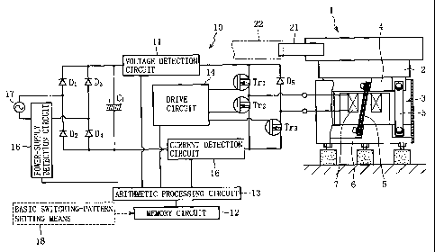
[0036A] [Fig. la] A circuit configuration diagram illustrating
a schematic configuration of a vibratory part feeder and a drive
control device thereof.
[Fig. lb] A plan view illustrating a part-transport path of a bowl
18
CA 02726167 2011-10-26
of the vibratory part feeder of Fig. la.
[Fig. lc] A schematic configuration diagram illustrating an
electromagnetic vibratory linear feeder.
[Fig. ld] A perspective view illustrating a projection nut which
is a part.
[Fig. 2] A flowchart illustrating steps of driving the vibratory
part feeder.
[Fig. 3] A flowchart illustrating processing steps by an arithmetic
processing circuit of the drive control device.
[Fig. 4] A waveform diagram illustrating an applied wave generated
by applying a half-wave voltage and a counter electromotive wave
generated by releasing a counter electromotive force generated on
an electromagnetic coil as a result of control of a power supply
voltage according to half-wave rectification.
[Fig. 5a] A waveform diagram illustrating a power supply voltage
serving as a reference.
[Fig. 5b] A waveform diagram illustrating a switching pattern based
on the reference voltage illustrated in Fig. 5a.
[Fig. 6a] A waveform diagram illustrating a power supply voltage
at a delivery destination.
[Fig. 6b] A waveform diagram illustrating a switching pattern based
on the power supply voltage illustrated in Fig. 6a.
Description of Embodiment
[00371 Detailed description is now given of the best mode for
19
CA 02726167 2011-10-26
embodying a drive control device for an oscillator according to
the present invention. Though a case of an application to an
electromagnetic vibratory part feeder using an oscillation generated
by an electromagnetic coil is exemplified in the following embodiment,
the present invention may be applied to a vibratory part feeder
using an oscillation generated by a piezoelectric element, an
electromagnetic vibratory linear feeder, an electromagnetic
vibratory part grinding device, and the like.
[0038] Fig. la illustrates a schematic configuration of a
vibratory part feeder 1 and a drive control device 10 therefor
according to the embodiment. Parts stored in the vibratory part
feeder 1 are iron projection nuts 19 as illustrated in Fig. ld,
and the projection nut is an ordinary one which has dimensions of
12 mm in length, 12 mm in width, and 5 mm in height, for example,
and which includes a threaded hole 19a formed at the center, and
projections for welding 19b formed at four corners on one side.
[0039] The vibratory part f eeder 1 according to this embodiment
includes a bowl 2 made of a steel plate. An oscillation generation
unit 3 is provided on a bottom side of the circular bowl 2 on which
a spiral part-transport path is formed. A spiral part-transport
path 20 (refer to Fig. lb) is formed along an inner wall surface
of the bowl 2. An attracted portion 4 which is made of a magnetic
material and fixed on a back surface of a bottom portion of this
bowl 2 is supported by top ends of a plurality of spring members
5, and bottom ends of the plurality of spring members 5 are fixed
CA 02726167 2011-10-26
at a predetermined inclined angle to a base member 6 in a stationary
state.
[0040] An electromagnetic coil 7 is provided on the base member
6, and the attracted portion 4 is intermittently attracted by turning
ON/OFF an electric power supplied to the electromagnetic coil 7,
thereby imparting a composed oscillation to the bowl 2 in a
circumferential direction and a vertical direction, and a large
number of the parts fed to the bottom portion of the bowl 2 are
sequentially transported along the part-transport path 20 in an
aligned form, and are fed out from a feed-out tube 21 on a top end
portion of the bowl 2. It should be noted that a gap at a predetermined
interval is provided between an electromagnetic iron core of the
electromagnetic coil 7 and the attracted portion 4, which is generally
provided and is thus not illustrated, resulting in the
above-mentioned composed oscillation.
[0041] The oscillation generation unit 3 of the vibratory part
feeder 1 is thus constructed by including the base member 6, the
spring members 5, the electromagnetic coil 7, and the attracted
portion 4 as a unit, and is locally the electromagnetic coil 7.
It should be noted that a transport slide surface of the part-transport
path 20 is connected to a transport slide surface of the feed-out
tube 21 as illustrated in Fig. lb.
[0042] A flexible feed tube 22 made of a urethane resin or a
polypropylene resin is connected to the feed-out tube 21 as
illustrated by long dashed double-short dashed lines in Figs. la
21
CA 02726167 2011-10-26
and lb, thereby feeding the projection nuts 19 to an electric
resistance welding machine, which is a consuming device for the
projection nuts 19, via a nut feeder device.
[0043] There is an electromagnetic vibratory linear feeder 23
as a device similar to the vibratory part feeder 1 as illustrated
in Fig. lc, and this feeder also has the problem relating to the
power supply voltage as mentioned above. The part-transport path
20 is formed on a linear part-transport member 24, and parts such
as bolts are transported along the part-transport path 20. This
transport is carried out by an oscillation as that provided by the
vibratory part feeder 1. If the parts are bolts, the bolts are
transported while the bolts are hanged from a head thereof . It should
be noted that like components are denoted by the same numerals as
those of Figs. la and 1b, and are not further described.
[0044] A main portion of the drive control device 10, which
controls the power supply to the electromagnetic coil 7 constituting
the oscillation generation unit 3 in the vibratory part feeder 1,
includes a voltage detection circuit 11, a memory circuit 12, an
arithmetic processing circuit 13, a drive circuit 14, a power-supply
detection circuit 15, and a current detection circuit 16. This drive
control device 10 converts the power supply voltage into a DC voltage
by rectifier diodes D1 to D4, which are connected to an AC power
supply 17 in a bridge configuration, and a smoothing capacitor C1,
converts the DC voltage into an output voltage by transistors Trl
to Tr3 serving as switching elements caused to carry out a switching
22
CA 02726167 2011-10-26
operation by the drive circuit 14, and drives the electromagnetic
coil 7 of the vibratory part feeder 1 by the output voltage thereof.
[0045] The voltage detection circuit 11 in the drive control
device 10 is provided on a subsequent stage of the rectifier diodes
D1 to D4 and the smoothing capacitor C1, and detects the DC voltage
obtained by the rectifier diodes D1 to D4 and the smoothing capacitor
C1 converting the power supply voltage input from the AC power supply
17, for example, a voltage value having a frequency of 60 Hz and
an amplitude of 200 V, as a power supply voltage at a delivery
destination.
[ 0046] A basic switching pattern in a case where the transistors
Tr1 to Tr3 are driven at a reference voltage with respect to the
power supply voltage at the delivery destination, for example, a
voltage value having a frequency of 60 Hz and an amplitude of 100
V, is stored in the memory circuit 12 in advance by
basic-switching-pattern setting means 18 in a production process
of the vibratory part feeder 1. This basic switching pattern is
a pattern in a good state or preferably an optimal state taking
into account the size and the mass of the projection nut 19, the
mass of the bowl 2, output characteristics of the electromagnetic
coil 7, and the like according to this embodiment, and is set in
the manufacturing stage so that the bowl 2 has an oscillation frequency
of 75 times per second at a voltage of 95 V for an optimal feeding
of approximately 200 pieces per minute in this embodiment.
[0047] The basic-switching-pattern setting means 18 provides
23
CA 02726167 2011-10-26
the function of setting the oscillation frequency of 75 times per
second and the voltage of 95 V for setting the amplitude as mentioned
above, for example, and various forms can be employed for the
basic-switching-pattern setting means 18. The following is an
example thereof. A device for setting the basic switching pattern
includes DC conversion means for converting the AC power supply
to a DC, waveform forming means for forming a predetermined waveform
from the DC, and means for setting this waveform to predetermined
frequency (oscillation frequency) andamplitude. Then, oscillation
frequency setting means for setting the frequency (oscillation
frequency) to the predetermined value is provided so as to be
adjustable, and amplitude setting means for setting the amplitude
to the predetermined value is provided so as to be adjustable.
[0048] The AC power supply is AC 100 V and 60 Hz, for example,
and is converted into the DC current, and is then set to proper
oscillation frequency and voltage (amplitude) by the oscillation
frequency setting means and the amplitude setting means. This
setting is the setting of optimal values through an operation on
adjustment dials or the like by an operator observing the number
of fed projection nuts, and the optimal values are the oscillation
frequency of 75 times per second and the voltage of AC 95 V for
this part feeder as mentioned before. The values obtained in this
way are stored in the memory circuit 12. This storage is carried
out according to an ordinary method using a computer device or the
like.
24
CA 02726167 2011-10-26
[0049] The arithmetic processing circuit 13 calculates a ratio
of the detected voltage output from the voltage detection circuit
11 to the reference voltage, and then calculates, based on the ratio,
a switching pattern substantially the same as the basic switching
pattern under an environment of the power supply voltage unique
to the delivery destination. In other words, ON/OFF timings are
calculated for a switching pattern substantially the same as the
basic switching pattern (oscillation frequency of 75 times per second
and voltage of 95 V) in a case where the transistors Tr1 to Tr3 are
driven at the reference voltage (voltage value having the frequency
of 60 Hz and the amplitude of 100 V) by multiplying a pulse width,
which represents ON/OFF timings of the basic switching pattern,
by the inverse of the ratio of the detected voltage to the reference
voltage as a switching pattern in a case where the transistors Tr1
to Tr3 are driven at the power supply voltage (voltage value having
the frequency of 60 Hz and the amplitude of 200 V) at the delivery
destination.
[0050] The drive circuit 14 converts the DC voltage converted
by the rectifier diodes D1 to D4 and the smoothing capacitor C1 to
the output voltage by the switching of the transistors Tr1 to Tr3
according to a control signal based on the calculation result by
the arithmetic processing circuit 13, and drives the electromagnetic
coil 7 of the vibratory part feeder 1 by using the output voltage.
[0051] It should be noted that the drive control device 10
includes the power-supply detection circuit 15 provided on the input
CA 02726167 2011-10-26
side of the AC power supply 17, and the current detection circuit
16 provided on the previous stage of the transistors Trl to Tr3.
[0052] The power-supply detection circuit 15 detects
presence/absence of the power supply by the AC power supply 17 in
order to restrain an inrush over current to the electromagnetic
coil 7 due to the start of the power supply after a short disconnection
of the power supply voltage. Moreover, the current detection circuit
16 detects the current flowing through the electromagnetic coil
7 in order to restrain an over current due to a damage or an overheat
of the electromagnetic coil 7.
[0053] Description is now given of an operation of the drive
control device 10 including the above-mentioned circuit
configuration based on flowcharts illustrated in Figs. 2 and 3 as
an example. Fig. 2 illustrates steps of driving the vibratory part
feeder 1, and Fig. 3 illustrates processing steps in the arithmetic
processing circuit 13 of the drive control device 10.
[0054] As illustrated in Fig. 2, first, the reference voltage
for driving the electromagnetic coil 7 of the vibratory part feeder
1 at a stable, constant oscillation is arbitrarily set, and the
basic switching pattern of the transistors Trl to Tr3 (ON/OFF timings
of the transistors Trl to Tr3) by the drive circuit 14 in a case
where the electromagnetic coil 7 is driven at the frequency of 60
Hz and the amplitude of 100 V, for example, is set by the
basic-switching-pattern setting means 18 in the production process
of the vibratory part feeder 1(STEP 1), and the basic switching
26
CA 02726167 2011-10-26
pattern is stored in the memory circuit 12 in advance (STEP 2).
The values stored in this way are AC 95 V and 75 Hz as illustrated
in Fig. 5b. The reference voltage set arbitrarily is selected from
a plurality of power supply voltages unique to delivery destinations.
[0055] On this occasion, in order to restrain the inrush over
current flowing to the electromagnetic coil 7 due to the start of
the power supply after the short disconnection of the power supply
voltage supplied by the AC power supply 17, the presence/absence
of the power supply by the AC power supply 17 is detected by the
power-supply detection circuit 15 (STEP 3) The arithmetic
processing circuit 13 makes a determination as described below based
on the output from the power-supply detection circuit 15. If the
power supply by the AC power supply 17 is present (power supply
is turned ON) , the power supply to the electromagnetic coil 7 continues
(STEP 4) , and if the power supply by the AC power supply 17 is not
present (power supply is turned OFF) , the power supply to the
electromagnetic coil 7 is disconnected, thereby stopping the drive
of the vibratory part feeder 1 (STEP 5) . In this way, the vibratory
part feeder 1 is protected against the inrush over current to the
electromagnetic coil 7.
[0056] Moreover, the current detection circuit 16 detects the
current flowing through the electromagnetic coil 7 in order to
restrain the over current due to the damage and the overheat of
the electromagnetic coil 7 (STEP 6). The arithmetic processing
circuit 13 makes a determination as described below based on the
27
CA 02726167 2011-10-26
output from the current detection circuit 16. If the over current
to the electromagnetic coil 7 is not generated, the power supply
to the electromagnetic coil 7 continues (STEP 7), and if the over
current to the electromagnetic coil 7 is generated, the power supply
to the electromagnetic coil 7 is disconnected, thereby stopping
the drive of the vibratory part feeder 1 (STEP 8), and reporting
the abnormal state by a lamp, a buzzer, or the like (STEP 9). In
this way, the vibratory part feeder 1 is protected against the over
current caused by the damage or the overheat of the electromagnetic
coil 7.
[0057] After it is confirmed whether or not the power supply
state of the electromagnetic coil 7 is normal as described above,
the drive circuit 14 causes the transistors Trl to Tr3 to carry out
the switching operation, thereby driving the electromagnetic coil
7 to impart the oscillation to the part-transport unit. On this
occasion, the arithmetic processing circuit 13 applies the control
according to half-wave rectification to the power supply voltage
from the AC power supply 17 as illustrated in Fig. 4, thereby
intermittently driving the electromagnetic coil 7 by repeating an
applied wave X generated by applying a half-wave voltage and a counter
electromotive wave Y generated by releasing a counter electromotive
force generated on the electromagnetic coil 7.
[0058] In other words, the arithmetic processing circuit 13
calculates a switching pattern which represents ON/OFF timings of
the transistors Trl to Tr3 by dividing a half wave of the DC voltage
28
CA 02726167 2011-10-26
rectified by the rectifier diodes D1 to D4 and the smoothing capacitor
C1 into fifteen divisions (equal divisions) (t1=t2=...=t14=t15) , for
example (STEP 10) , and the transistors Tr1 to Tr3 are caused to carry
out the switching operation as described below (STEP 11).
[0059] As illustrated in an enlarged view of a portion A of
Fig. 4, the transistors Tr1 and Tr3 (refer to Fig. la) are turned
ON in a period b of the applied wave X for applying the voltage,
and the transistors Tr2 and Tr3 are turned ON in a period a of the
applied wave X for not applying the voltage. The period a and the
period b of the applied wave X are adjusted in terms of time on
this occasion. In other words, an effective sine wave (thin line
of Fig. 4) is generated based on a switching pattern in which ON
time (period b) or OFF time (period a) is gradually decreased or
increased so that the ON time (period b) is maximum and the OFF
time (period a) is minimum at the center of the fifteen divisions
(tl=t2= . . . =t14=t15) , and the ON time (period b) is minimum and the
OFF time (period a) is maximum on both end portions thereof.
[0060] In this case, the each period of the fifteen divisions
(t1=t2=...=t14=t15) may be set constant, and the ON time (period b)
may be increased/decreased. It should be note that the each period
of the fifteen divisions (t1=t2=...=t14=t15) may be set constant,
and the OFF time (period a) may also be increased/decreased.
[0061] As illustrated in an enlarged view of a portion B of
Fig. 4, only the transistor Tr2 is turned ON in a period b' of the
counter electromotive wave Y for releasing the counter electromotive
29
CA 02726167 2011-10-26
force, and the transistors Tr2 and Tr3 are turned ON in a period
a' of the counter electromotive wave Y for not releasing the counter
electromotive force. The period a' and the period b' of the counter
electromotive wave Y are adjusted in terms of time on this occasion.
In other words, the effective sine wave (thin line of Fig. 4) is
generated based on a switching pattern in which the ON time (period
b' ) or the OFF time (period a' ) is gradually decreased or increased
so that the ON time (period b' ) is maximum and the OFF time (period
a') is minimum at the center of the fifteen divisions
(t' 1=t' 2=... =t' 14=t' 15) , and the ON time (period b' ) is minimum and
the OFF time (period a') is maximum on both end portions thereof.
[0062] In this case, the each period of the fifteen divisions
(t1' =t2' _ . . . =t14' =t15' ) may be set constant, and the ON time (period
b') may be increased/decreased. It should be noted that the each
period of the fifteen divisions (t1' =t2' =... =t14' =t15' ) may be set
constant, and the OFF time (period a') may also be
increased/decreased.
[0063] In this way, the control according to the half-wave
rectification is applied to the power supply voltage from the AC
power supply 17, thereby supplying the electromagnetic coil 7 with,
as the output voltage of the drive control device 10, the effective
sine wave generated based on the switching pattern repeating the
applied wave X generated by applying the half-wave voltage and the
counter electromotive wave Y generated by releasing the counter
electromotive force generated on the electromagnetic coil 7. As
CA 02726167 2011-10-26
a result, the electromagnetic coil 7 is intermittently driven using
the output voltage. The half-wave rectification of the power supply
voltage can impart a stronger oscillation to the part-transport
unit than control according to full-wave rectification applied to
the power supply voltage, and hence power can be saved.
[0064] The drive control device 10 can cause the electromagnetic
coil 7 of the vibratory part feeder 1 to always generate a constant
oscillation for the predetermined voltage range (such as 90 V to
260 V) including a plurality of types of power supply voltages
different in frequency and amplitude from the reference voltage
(frequency of 60 Hz and amplitude of 100 V, for example) depending
on the delivery destination which is the location at which the
vibratory part feeder 1 is to be installed.
[0065] For example, Fig. 5a illustrates a reference voltage
having a frequency of 60 Hz and an amplitude of 100 V as an example,
and Fig. 6a illustrates a power supply voltage unique to a delivery
destination having a frequency of 60 Hz, and an amplitude of 200
V as an example. In this case, the drive control device 10 detects
the power supply voltage (in a case of frequency of 60 Hz and amplitude
of 200 V illustrated in Fig. 6a) unique to the delivery destination
of the vibratory part feeder 1 by the voltage detection circuit
11 (refer to Fig. la) as illustrated in Fig. 3 (STEP 1), and the
arithmetic processing circuit 13 calculates the ratio of the
detection voltage (power supply voltage unique to the delivery
destination) output from the voltage detection circuit 11 to the
31
CA 02726167 2011-10-26
reference voltage (in a case of frequency of 60 Hz and amplitude
of 100 V illustrated in Fig. 5a) (the detection voltage is twice
as high in amplitude as the reference voltage in this case) (STEP
2).
[0066] On this occasion, in the arithmetic processing circuit
13, as described above, the effective sine wave (thin line of Fig.
5b) is generated based on the switching pattern which represents
the ON/OFF timings of the transistors Tr1 to Tr3, in which the half
wave of the DC voltage rectified by the rectifier diodes D1 to D4
and the smoothing capacitor C1 is divided into the fifteen divisions
(equal divisions), for example, and then the ON time (period b)
or the OFF time (period a) is gradually decreased or increased so
that the ON time (period b) is maximum and the OFF time (period
a) is minimum at the center of the fifteendivisions (t1=t2=. = .=t14=t15) ,
and the ON time (period b) is minimum and the OFF time (period a)
is maximum on both end portions thereof. In this case, the each
period of the fifteen divisions (tl=t2=...=t14=t15) is set constant,
and the ON time (period b) is increased/decreased.
[0067] Then, the basic switching pattern (corresponding to the
reference voltage) of the transistors Tr1 to Tr3 stored in advance
in the memory circuit 12 is read from the memory circuit 12 (STEP3)
and the ON/OFF timings are calculated, based on the above-mentioned
ratio, for the switching pattern substantially the same as the basic
switching pattern (oscillation frequency of 75 times per second
and voltage of 95 V) for driving the transistors Tr1 to Tr3 at the
32
CA 02726167 2011-10-26
reference voltage (voltage value having the frequency of 60 Hz and
the amplitude of 100 V) by multiplying the pulse width (on period
(period b)), which represents the ON/OFF timings of the basic
switching pattern, by the inverse of the ratio of the detected voltage
to the reference voltage as a switching pattern in a case where
the transistors Trl to Tr3 are driven at the power supply voltage
(voltage value having the frequency of 60 Hz and the amplitude of
200 V) at the delivery destination.
[0068] Specifically, the frequency and the amplitude of the
reference voltage are 60 Hz and 100 V while the frequency and the
amplitude of the power supply voltage at the delivery destination
are 60 Hz and 200 V, and hence the amplitude of the power supply
voltage, which is the detection voltage, is twice as high as the
amplitude of the reference voltage (ratio is 2) . Accordingly, the
ON time obtained by dividing the half wave (refer to Fig. 5b) of
the reference voltage by fifteen is multiplied by 1/2, which is
the inverse of the ratio (STEP 4), and the OFF time is multiplied
by two, which is the ratio (STEP 5). It should be noted that if
the half wave is not finished (STEP 6), the above-mentioned ratio
calculation is to be repeated.
[0069] This results in a half wave of the power supply voltage
in which the ON times of the half wave of the reference voltage
are halved and the OFF times are doubled. In other words, the
switching pattern at the delivery destination illustrated in Fig.
6b is obtained by halving the ON times of the basic switching pattern
33
CA 02726167 2011-10-26
illustrated in Fig. 5b and doubling the OFF times. As a result,
the effective sine wave (frequency of 75 Hz and amplitude of 95
V) based on the switching pattern for the power supply voltage at
the delivery destination as illustrated by a thin line of Fig. 6b
is substantially the same as the effective sine wave (frequency
of 75 Hz and amplitude of 95 V) based on the basic switching pattern
for the reference voltage as illustrated by the thin line of Fig.
5b.
[0070] As described above, the ON times and the OFF times
obtained by diving by fifteen are changed according to the ratio
of the power supply voltage to the reference voltage, thereby making
the effective sine wave based on the switching pattern for the power
supply voltage at the delivery destination and the effective sine
wave based on the basic switching pattern for the reference voltage
substantially the same. Then, the effective sine wave is supplied
as the output voltage of the drive control circuit 10 to the
electromagnetic coil 7 of the vibratory part feeder 1, therebydriving
the electromagnetic coil 7 using the output voltage. A good or
optimal, constant oscillation can always be generated by the
electromagnetic coil 7 of the vibratory part feeder 1 in this way.
[0071] It should be noted that the transistors Trl to Tr3 are
driven by the drive circuit 14 according to the control signal output
from the arithmetic processing circuit 13 based on the output from
the voltage detection circuit 11 always monitoring and detecting
the power supply voltage at the delivery destination. Thereal-time
34
CA 02726167 2011-10-26
monitoring as described above of the power supply voltage secures
the generation of the always constant oscillation by the
electromagnetic coil 7 of the vibratory part feeder 1, and thus
enables quick adaptation to a change in power supply voltage. A
proper reaction by the arithmetic processing is further provided
for a slight variation in power supply voltage caused by the electric
power used in a plant, and the constant oscillation can always be
generated.
[0072] Further, if the vibratory part feeder 1 is put into
practical use as a part feeding device, the number of projection
nuts to be fed can be adapted to the number thereof to be consumed
by an electrical resistance welder or the like, and a proper
relationship with a subsequent process can be established, resulting
in stable production management.
Example 1
[0073] The applicant carried out an experiment on the number
of fed parts in response to a variation in power supply voltage,
on the vibratory part feeder 1 having the following specifications.
[ 0074 ] The diameter of the bowl 2 of the vibratory part feeder
1 is 28 cm, the mass thereof is 2 kg, and the part is the projection
nut 19 dimensioned as mentioned before. The above-mentioned
reference voltage is AC 100 V, the frequency is 60 Hz, and the basic
switching pattern stored in the memory circuit 12 is AC 95 V and
75 Hz as effective values.
[0075] The power supply voltage was increased from AC 90 V
CA 02726167 2011-10-26
successively by 10 V each time under this condition, and the number
of nuts fed from the feed-out tube 21 was measured at each of the
voltages. Results thereof are as follows.
155 to 160 per minute at AC 90 V
194 to 204 per minute at AC 100 V
204 to 218 per minute at AC 110 V
200 to 202 per minute at AC 120 V
194 to 214 per minute at AC 130 V
188 to 202 per minute at AC 140 V
180 to 184 per minute at AC 180 V
170 to 206 per minute at AC 230 V
174 to 194 per minute at AC 260 V
[0076] It was confirmed that those fed numbers are sufficient
for a subsequent operation cycle of an electric resistance welder.
It should be noted that the numbers are shown by an increment of
V up to AC 140 V, but subsequent numbers are close to each other
and are thus shown by an increment of 30 V or more. Moreover, the
projection nut 19 has the form having the projections for welding
19b formed at the four corners on one side as illustrated in Fig.
id, thus has a front side and a rear side, and is normally transported
on the part-transport path 20 in the bowl 2 while the front side
is facing upward, but a situation in which the projection nut 19
is in a state in which the rear side is facing upward as a result
of an oscillation and is not transported on the part-transport path
may occur, which causes a variation in the fed number. In other
36
CA 02726167 2011-10-26
words, the variation in the fed number occurs in a case where the
number of the projection nuts 19 with the front side facing upward
is larger than the number of the projection nuts 19 with the rear
side facing upward on the part-transport path 20, or in an opposite
case thereof.
[ 0077 ] On the other hand, as a comparative example, a bowl having
the same dimensions and the mass was used, the same projection nuts
were used as parts, and a vibratory part feeder without the drive
control circuit according to the present invention was operated.
In this case, the power supply voltage is AC 100 V and 60 Hz. Results
thereof are as follows.
164 to 194 per minute at AC 100 V
82 to 102 per minute at AC 90 V
100 to 120 per minute at AC 110 V
[0078] The case of AC 100 V was within a proper range in terms
of the fed number as shown above. However, the transport speed of
the nuts was too slow at AC 90 V, resulting in an extremely decreased
fed number, and the oscillation state was too strong and thus the
nuts fell off from the part-transport path 20 at AC 110 V, resulting
in an extremely decreased fed number. Observation of this
comparative example reveals that the change in power supply voltage
to AC 90 V or AC 110 V immediately causes a drastic reduction in
fed number, and the vibratory part feeder fails in terms of the
nut-feeding capability to the electric resistance welder due to
an absence of an automatic response feature to the change in power
37
CA 02726167 2011-10-26
supply voltage.
[0079] The amplitude and the frequency of the reference voltage
are AC 100 V and 60 Hz. However, if the vibratory part feeder 1
was operated while connected to a power supply of AC 10O V and frequency
of 50 Hz, that is, if a test was carried out assuming a case where
only the frequency is different such as a difference in frequency
between the Kansai area and the Kanto area in Japan, the number
of nuts fed from the feed-out tube 21 was 190 to 205 per minute,
which is sufficient number for the electric resistance welder in
the subsequent process.
[0080] On the other hand, if the vibratory part feeder without
the drive control circuit according to the present invention was
operated, the number of nuts fed from the feed-out tube 21 drastically
decreased to 40 to 50 per minute, which revealed an insufficient
feeding capability to the electric resistance welder. Thereference
voltage and the power supply voltage at the delivery destination
are the same in a case where the amplitude of the power supply voltage
does not change and only the frequency changes as described above
in the example, and hence a ratio of the reference voltage to the
power supply voltage at the delivery destination is 1, and the basic
switching pattern is reproduced.
[0081] The basic-switching-pattern setting means 18 is
provided as a production device or a production facility for storing
the basic switching pattern in the memory circuit 12 in the embodiment
illustrated in Fig. la and the like. However, the
38
CA 02726167 2011-10-26
basic-switching-pattern setting means 18 and a circuit required
for the storage (such as a simplified computer device) may be built
into the drive control device 10 of a vibratory part feeder or the
like, which is an oscillator, the proper oscillation frequency and
amplitude may be set by the built-in means 18, and then the means
18 may be made into a black box or the adjusting dial may be locked
(by caulking, for example) so that the customer cannot convert those
set values, thereby utilizing the purport of the present invention.
The employment of this method enables maintaining a large number
of vibratory part feeders along with the drive control device 10
in stock, and setting a proper basic switching pattern according
to the part mass and the size of the bowl requested by the customer
immediately before the delivery in an adjustment process on a
delivering factory. In other words, the oscillation frequency and
the amplitude can be properly set according to the request from
the customer in the logistics process of the production and the
delivery.
[0082] The present invention is not limited to the
above-mentioned embodiment, and it is understood that the present
invention may be embodied in further various forms without departing
from the gist of the present invention, and the scope of the present
invention is defined by claims, and includes all equivalents
mentioned in the claims and all modifications within the scope.
Industrial Applicability
39
CA 02726167 2011-10-26
[0083] As described above, according to the present invention,
predetermined frequency and amplitude proper for the oscillator
are automatically secured only by connecting the oscillator to the
power supply even if the power supply voltage varies at the delivery
destination of the oscillator, and hence it is not necessary for
a customer to carry out a special adjustment operation or the like,
and it is expected that the oscillator be widely used in a process
for electric resistance welding of an automobile body and the like.
Reference Signs List
[0084] 1 vibratory part feeder
7 oscillation generation unit (electromagnetic coil)
drive control device
11 voltage detection circuit
12 memory circuit
13 arithmetic processing circuit