Note : Les descriptions sont présentées dans la langue officielle dans laquelle elles ont été soumises.
CA 02754098 2011-09-27
P6332CA00 30
August 2011
1/
DETECTION OF A CONTACTLESS DATA STORAGE DEVICE
Field of the Invention
The present invention relates to a detection circuit and a method for
detecting a
contactless data storage device within a communication range of an antenna.
Specifically, the present invention relates to a detection circuit and a
method for
detecting within a communication range of an antenna for emitting an
electromagnetic
field a contactless data storage device which is configured for inductive
coupling with
the electromagnetic field.
Background of the Invention
Data storage devices such as smart cards or identification tags which can be
accessed
without any electrical contact for reading and/or writing purpose have become
increasingly popular. Particularly, for person or product identification
applications radio
frequency identification (RFID) systems are in widespread use. In RFID
systems,
contactless communication between a contactless data storage device and a
reader or
read/write device is based on inductive coupling of a RF field, i.e. an
electromagnetic
field which is emitted by an antenna of the read/write device, and a
conductive object,
typically a coil integrated in the data storage device. Inductive coupling
occurs within
the communication range of the reader device, i.e. in the vicinity of the
antenna, as
soon as the RF field is switched on. Accordingly, for detecting, identifying
and/or
authenticating a passive contactless data storage device within the
communication
range of the read/write device, the RF field is switched on periodically, e.g.
every 250
milliseconds, a modulated identification/authentication signal with a duration
of a few
milliseconds is emitted, and a response from the data storage device is
detected. In
setups where the read/write device is not connected to electrical power lines
but relies
on batteries, the periodic emission of the identification/authentication
signal is
inefficient because it consumes too much electrical power, particularly, when
no data
storage device is present. Ideally, the identification/authentication signal
would only be
CA 02754098 2011-09-27
P6332CA00 30
August 2011
2/
emitted, if a contactless data storage device is present within the
communication range
of the read/write device.
WO 03/052672 describes a contactless integrated circuit reader comprising a
tuned
antenna for emitting a magnetic field and means for detecting the presence of
a
contactless integrated circuit, comprising a coil, within a communication
perimeter of
the reader. According to WO 03/052672, short magnetic field pulses having a
duration
of 10-50ps are emitted and by way of a data receiving circuit, which comprises
a
rectifying diode and a low pass filter, an envelope signal having envelope
pulses
corresponding to the magnetic field pulses is extracted at the antenna. The
amplitude
of the envelope pulses is monitored and, if at least one envelope pulse has an
amplitude below a detection threshold, an object is assumed to have been
introduced
into the communication perimeter. Subsequently, a normal
identification/authentication
request signal is emitted so as to determine whether the object that has
entered the
communication perimeter is a contactless device or not. The method of WO
03/052672
requires a receiving circuit to generate the envelope pulses, before the
presence of a
contactless device can be detected.
US 7,598,872 describes a method for detecting identification media within the
communication range of an antenna for transmitting and receiving RF signals of
a
read/write unit which operates in accordance with the principle of inductive
coupling of
an RF field in the MHz frequency band, e.g. 10 MHz. According to US 7,598,872
a
short polling signal, e.g. 5ps, which is much shorter than the normal
identification/authentication signal and contains a number of fundamental
(carrier)
oscillations of the RF field, is periodically emitted via the antenna. In
order to avoid the
transient phase of amplitude build-up of the carrier oscillation at the
beginning of the
polling signal, a return signal with a number of stable fundamental
oscillations of the RF
field is detected at the antenna at a defined time delay, after the beginning
of the
emission of the polling signal, for example, in the second half of the polling
signal, e.g.
after a time delay of 3ps. Subsequently, the detected return signal is
compared to a
CA 02754098 2011-09-27
P6332CA00 30
August 2011
3/
reference signal, and if the return signal differs from the reference signal,
an
identification medium is assumed to be within the communication range of the
antenna,
and a normal identification/authentication request signal is emitted for
detecting,
identifying and/or authenticating the identification medium. Within the delay
time,
settling processes can take place so that in the detected measurement range
the
detected return signal includes only stable fundamental oscillations. On one
hand,
limiting the return signal to stable oscillations requires a time delay in the
detection
process; while on the other hand, the return signal can be compared to the
reference
signal, before the end of the polling signal.
Summary of the Invention
It is an object of this invention to provide a detection circuit and a method
for detecting
within a communication range of an antenna, for emitting an electromagnetic
field, a
contactless data storage device, configured for inductive coupling with the
electromagnetic field, which detection circuit and detection method do not
have at least
some of the shortcomings of the prior art. In particular, it is an object of
the present
invention to provide a detection circuit and a detection method which do not
necessarily
require receiving circuits to generate envelope pulses, before the presence of
a
contactless device can be detected. In particular, it is another object of the
present
invention to provide a detection circuit and a detection method which do not
require a
time delay for limiting the detection to stable carrier oscillations.
According to the present invention, these objects are achieved through the
features of
the independent claims. In addition, further advantageous embodiments follow
from the
dependent claims and the description.
A contactless data storage device, e.g. an identification medium, is
configured for
inductive coupling with an electromagnetic field emitted by an antenna, e.g.
an antenna
of a reader or read/write device. For detecting the contactless data storage
device
within a communication range of the antenna, a detection circuit has a
connector for
CA 02754098 2011-09-27
P6332CA00 30
August 2011
4/
connecting to the antenna and for detecting a return signal at the antenna
during
emission of an electromagnetic field pulse. In the present context, the term
"return
signal" refers to a signal which is the sum of forward and reflected wave (at
the
antenna).
According to the present invention, the above-mentioned objects are
particularly
achieved in that the detection circuit for detecting the contactless data
storage device
within the communication range of the antenna is further configured to
generate, during
amplitude build-up of carrier oscillation at the beginning of the
electromagnetic field
pulse, an evaluation signal based on the return signal, and to detect the data
storage
device within the communication range based on a threshold value and the
evaluation
signal generated during the amplitude build-up. By detecting the presence of
the data
storage device based on an evaluation signal generated in the transient phase
of
amplitude build-up of the carrier oscillation at the beginning of the
electromagnetic field
pulse, the detection of the data storage device can be initiated before
carrier oscillation
of the electromagnetic field pulse is stable. Consequently, the width of the
electromagnetic field pulse can be shortened and, therefore, energy
consumption for
detecting the presence of the data storage device can be reduced.
In a preferred embodiment, the detection circuit is configured to determine
based on
the evaluation signal the slope of the amplitude build-up, and to detect the
data storage
device within the communication range based on the threshold value and the
slope of
the amplitude build-up. Specifically, the data storage device is detected when
the slope
of the amplitude build-up significantly changes (decreases or increases)
between
consecutive electromagnetic field pulses.
In a further preferred embodiment, the detection circuit is configured to
generate the
evaluation signal as a comparative signal, during amplitude build-up of the
carrier
oscillation at the beginning of the electromagnetic field pulse, based on a
comparison
of the return signal and a comparative value, and to detect the presence of
the data
CA 02754098 2011-09-27
P6332CA00 30
August 2011
5/
storage device based on the comparative signal generated during the amplitude
build-
up and the threshold value.
In an embodiment, the detection circuit is configured to generate the
comparative
signal to indicate exceeding oscillations of the return signal, exceeding
oscillations
having in each case an amplitude greater than the comparative value, and to
detect the
presence of the data storage device based on the number of exceeding
oscillations
within a defined time interval during the amplitude build-up. Essentially, the
number of
exceeding oscillations within the defined time interval during the amplitude
build-up is a
measure of the slope of the amplitude build-up.
In a further embodiment, the detection circuit comprises an Analog-Digital-
converter
and a Villard circuit for connecting the antenna to an input of the Analog-
Digital-
converter. The Villard circuit is configured to generate the evaluation
signal, during
amplitude build-up of carrier oscillation at the beginning of the
electromagnetic field
pulse, through transposition of the return signal from the antenna to a
defined operating
range of the Analog-Digital-converter. The detection circuit is configured to
detect the
presence of the data storage device based on a digital value generated by the
Analog-
Digital-converter from the evaluation signal provided at a defined point in
time during
amplitude build-up. Accordingly, the Villard circuit provides a measure of the
return
signal by building up a respective charge in a capacitor, and the value of the
built-up
charge at a defined point in time during amplitude build-up is a measure of
the slope of
the amplitude build-up.
In another embodiment, the detection circuit is configured to generate the
comparative
signal to indicate the phasing of the return signal, to determine a phase
shift between
the comparative signal and carrier oscillations of the electromagnetic field
pulses, and
to detect the presence of the data storage device based on the phase shift and
the
threshold value.
CA 02754098 2011-09-27
P6332CA00 30
August 2011
6/
In a variant, the detection circuit comprises an Exclusive-Or element for
generating
from the comparative signal and the carrier oscillation of the electromagnetic
field
pulses a phase signal indicative of the phase shift between the comparative
signal and
the carrier oscillation of the electromagnetic field pulses, and the detection
circuit is
configured to determine for an electromagnetic field pulse an average phase
shift from
the phase signal, and to detect the presence of the data storage device based
on the
average phase shift of electromagnetic field pulses and the threshold value.
Preferably, the detection circuit is configured to detect the data storage
device based
on an upper threshold value, indicative of a reinforcing effect of an object
in the
communication range, and a lower threshold value, indicative of an attenuating
effect of
an object in the communication range. For example, a slope of the amplitude
build-up
greater than the upper threshold value indicates the reinforcing effect of an
object in
the communication range, whereas a slope of the amplitude build-up smaller
than the
lower threshold value indicates the attenuating effect of an object in the
communication
range. Specifically, a number of exceeding oscillations above the upper
threshold value
indicates the reinforcing effect of a present object, whereas a number of
exceeding
oscillations below the lower threshold value indicates the attenuating effect
of a present
object. Accordingly, a phase shift above the upper threshold value indicates
the
reinforcing effect of a present object, whereas a phase shift below the lower
threshold
value indicates the attenuating effect of a present object.
Preferably, the detection circuit is configured to define dynamically
threshold values
depending on the evaluation signal generated during the amplitude build-up of
a
previously emitted electromagnetic field pulse.
In addition to the detection circuit for detecting the contactless data
storage device
within the communication range of the antenna, the present invention further
relates to
a method of detecting within the communication range of an antenna for
emitting an
electromagnetic field a contactless data storage device which is configured
for
CA 02754098 2011-12-23
- .
7/
inductive coupling with the electromagnetic field. During emission of an
electromagnetic field pulse, a return signal is detected at the antenna.
During
amplitude build-up of the carrier oscillation at the beginning of the
electromagnetic field
pulse, an evaluation signal is generated based on the return signal. The data
storage
device is detected within the communication range based on a threshold value
and the
evaluation signal generated during the amplitude build-up.
Preferably, the slope of the amplitude build-up is determined based on the
evaluation
signal, and the data storage device is detected within the communication range
based
on the threshold value and the slope of the amplitude build-up.
In an embodiment, the evaluation signal is generated as a comparative signal,
during
amplitude build-up of the carrier oscillation at the beginning of the
electromagnetic field
pulse, based on a comparison of the return signal and a comparative value. In
a
variant, the comparative signal indicates exceeding oscillations of the return
signal
having an amplitude greater than the comparative value, and the presence of
the data
storage device is detected based on the number of exceeding oscillations
within a
defined time interval during the amplitude build-up. In another variant, the
comparative
signal indicates the phasing of the return signal. The phase shift between the
comparative signal and carrier oscillations of the electromagnetic field
pulses are
determined, and the presence of the data storage device is detected based on
the
phase shift and the threshold value.
In another embodiment, the antenna is connected via a Villard circuit to an
input of an
Analog-Digital-converter, and the evaluation signal is generated, during
amplitude
build-up of the carrier oscillation at the beginning of the electromagnetic
field pulse, by
the Villard circuit performing current integration and transposition of the
return signal
from the antenna to a defined operating range of the Analog-Digital-converter.
The
presence of the data storage device is detected based on a digital value
generated by
CA 02754098 2011-12-23
7a/
the Analog-Digital-converter from the evaluation signal provided at a defined
point in
time during amplitude build-up.
CA 02754098 2011-09-27
P6332CA00 30
August 2011
8/
Brief Description of the Drawings
The present invention will be explained in more detail, by way of example,
with
reference to the drawings in which:
Figure 1: shows a block diagram illustrating schematically a read/write device
with a
detection circuit for detecting a contactless data storage device within the
communication range of an antenna of the read/write device.
Figure 2a: shows a graph of a return signal detected at the antenna, during
amplitude
build-up of the carrier oscillation at the beginning of an electromagnetic
field
pulse, when there is no device in the electromagnetic field emitted by the
antenna.
Figure 2b: shows a graph of the return signal during amplitude build-up when
there is
a device having an attenuating effect in the electromagnetic field emitted by
the antenna.
Figure 2c: shows a graph of the return signal during amplitude build-up when
there is
a device having a reinforcing effect in the electromagnetic field emitted by
the antenna.
Figure 3: shows a block diagram illustrating schematically a read/write device
with
another embodiment of a detection circuit for detecting a contactless data
storage device within the communication range of the antenna.
Figure 4: shows a timing diagram illustrating the course of an oscillating
signal
representing carrier oscillations of the electromagnetic field pulse, a
comparative signal representing the phasing of the return signal detected at
the antenna, and a phase shift signal indicating the phase shift between the
oscillating signal and the comparative signal.
CA 02754098 2011-09-27
P6332CA00 30
August 2011
9/
Figure 5a: shows a graph of the return signal detected at the antenna, during
amplitude build-up of the carrier oscillation at the beginning of an
electromagnetic field pulse, when there is no device in the electromagnetic
field emitted by the antenna.
Figure 5b: shows a graph of the return signal during amplitude build-up when
there is
a device having a positive phase shifting effect in the electromagnetic field
emitted by the antenna.
Figure 5c: shows a graph of the return signal during amplitude build-up when
there is
a device having a negative phase shifting effect in the electromagnetic field
emitted by the antenna.
Figure 6: shows a block diagram illustrating schematically a read/write device
with an
embodiment of the detection circuit having a Villard circuit for integrating
the return signal.
Figure 7: shows a graph of the return signal detected at the antenna, during
amplitude build-up of the carrier oscillation at the beginning of an
electromagnetic field pulse, and an evaluation signal generated through
current integration which indicates the slope of the amplitude build-up.
Figure 8: shows a flow diagram illustrating various exemplary sequences of
steps for
detecting a contactless data storage device within the communication
range of the antenna of the read/write device.
Detailed Description of the Preferred Embodiments
In Figures 1, 3 and 6, reference numeral 1 refers to a reader and/or a
read/write
device, hereinafter collectively referred to as "reader", configured and
operable to read
and/or write data from/to a contactless data storage device 2 through
inductive
CA 02754098 2011-09-27
P6332CA00 30
August 2011
10/
coupling with an electromagnetic field or an electromagnetic field pulse
emitted by the
antenna 4 of the reader 1.
As illustrated schematically in Figures 1, 3 and 6, the contactless data
storage device
2, hereinafter referred to as "contactless device", comprises an antenna coil
20 for
inductive coupling with the electromagnetic field of the reader 1. The antenna
coil 20 is
connected to a microchip which includes a data store containing stored data,
e.g.
product or user identification data. For example, the contactless device is an
RFID tag
or an RFID transponder, implemented in the form of a label, (smart) card,
bracelet, key
tag, etc. For example, the reader 1 is an RFID reader interacting with the
contactless
device 2 according to a standardized RFID protocol as defined in standards
such as
ISO 18092, ISO 15693, or ISO 14443, or according to a proprietary data
transmission
or RFID protocol. For example, the reader 1 is operating with an
electromagnetic field 3
or electromagnetic field pulses 30 having a carrier frequency in the range of
100 KHz to
2.5GHz. Particularly, the carrier frequency is set to the working frequency of
an RFID
system, e.g. 6.78MHz, 13.56MHz, or 27.12MHz (or another multiple of 13.56MHz).
As illustrated schematically in Figures 1, 3 and 6, the reader comprises a
detection
circuit 10 for detecting the presence of a contactless device 2 within the RF
communication range of the reader 1 or its antenna 4, respectively. The
detection
circuit 10 is connected electrically via a connector to the antenna 4 for
detecting a
return signal during a short electromagnetic field pulse 30, emitted by the
reader 1 as a
polling signal via its antenna 4, as will explained below in more detail.
Furthermore, the
detection circuit 10 comprises a processing unit 13 for determining whether
there is a
contactless device 2 in the communication range, by processing the detected
return
signal or a corresponding signal or value derived from the return signal by
various
circuits and/or components. For example, the processing unit 13 comprises a
microprocessor with stored program modules, or another programmed logic unit.
CA 02754098 2011-09-27
P6332CA00 30
August 2011
11/
In the embodiment of Figure 1, the detection circuit 10 further comprises an
input buffer
15, an RC-circuit for connecting the input buffer 15 to the antenna 4, a
counter 12
connected to the output of the input buffer15 and to the processing unit 13, a
timer 14
connected to the counter 12 and the processing unit 13, and a threshold module
11
connected to the input buffer 15. As shown in Figure 1, the antenna 4 is
connected via
capacitor C to the input of the input buffer 15.
The threshold module 11, e.g. a Digital/Analog converter, is connected via
resistor R to
the input of the input buffer 15 and configured to set a threshold voltage
Vthresh. In a
variant, the threshold module 11 is part of the processing unit 13.
Preferably, the input
buffer 15 is configured as a hysteresis input buffer generating a comparative
output
signal Ucomp with a high output level when the antenna voltage Uant exceeds
the
comparative value set by the threshold voltage Vthresh, and a low output level
when
the antenna voltage Uant reverts to a level at or below the comparative value
set by the
threshold voltage Vthresh, e.g. zero.
For example, the electromagnetic field pulse 30 has a pulse width tp which is
set, for
example, to a length or duration in the range of 1ps to 5ps, e.g. 3 ps, and is
thus
considerably shorter than a normal identification or authentication signal of
a standard
RFID reader which is typically in the order of a few milliseconds. As is
illustrated
schematically, in Figures 2a, 2b, 2c, 5a, 5b and 5c, the electromagnetic field
pulse 30
(polling signal) has a transient amplitude build-up phase at the beginning of
the
electromagnetic field pulse 30 where carrier oscillations of the
electromagnetic field
pulse 30 build up their amplitude to the full maximum amplitude A of stable
oscillations
at time ta, e.g. ta ?_50Ons . As will be outlined below, the return signal
Uant detected at
the antenna 4 will be evaluated and analyzed during the amplitude build-up,
within an
evaluation time interval [0, tm].
Generally, the relationship between the evaluation time (interval) tm, the
amplitude
build-up time ta (i.e. the rise time), and the pulse width tp is defined as tm
ta tp.
CA 02754098 2011-09-27
P6332CA00 30
August 2011
12/
However, for a slow build-up time ta, e.g. ta.2,us , depending on the Q-rating
of the
antenna, the measurement may be initiated at a time ta' during amplitude build-
up,
before the full maximum amplitude A of stable oscillations is reached at time
ta.
Preferably, the evaluation time tm and the pulse width tp have the same
duration
tin =tp . In a preferred configuration, the evaluation time tm, the amplitude
build-up
time ta (rise time), and the pulse width tp have the same duration tin =ta =tp
, e.g.
tm =ta=tp=2ps or tm =ta=tp=3ps; or for slow rising scenarios tm =ta1= tp, e.g.
tm = ta'= tp =2,us or tm = ta'=tp=3ps . Table 1, summarizes the various
configurations for different embodiment scenarios:
Configuration Corresponding scenario
Evaluation occurs during amplitude build-
tm < ta and ta <tp up, before stable oscillation is reached.
The magnetic field pulse includes stable
oscillations.
Evaluation occurs during amplitude build-
tm = ta and ta <tp up, until stable oscillation is reached. The
magnetic field pulse includes stable
oscillations.
Evaluation occurs during amplitude build-
tm < ta and ta =
up, before stable oscillation is reached.
tp
The magnetic field pulse includes only the
amplitude build-up, without any stable
oscillations.
Evaluation occurs during amplitude build-
tm = ta =tp up, until stable oscillation is reached. The
magnetic field pulse includes only the
amplitude build-up, without any stable
oscillations.
Evaluation occurs during amplitude build-
up, before stable oscillation is reached.
tm = tp = tat < ta
The magnetic field pulse includes only
part of the amplitude build-up, without any
stable oscillations.
Table 1
CA 02754098 2011-09-27
P6332CA00 30
August 2011
13/
The counter 12 is configured to count the number of oscillations of the return
signal that
exceed the voltage threshold Vthresh during the transient amplitude build-up
phase [0,
ta] of the electromagnetic field pulse 30 of the reader's polling signal,
within a defined
time period tm from the beginning of the electromagnetic field pulse 30.
At the end of the defined time period tm, the number of exceeding oscillations
are read
by the processing unit 13 and the counter 12 is reset, for example.
Subsequently, the
processing unit 13 determines whether or not a contactless device 2 (or
another object)
is within the antenna's communication range by comparing the current number of
oscillations to an upper threshold, indicative of a reinforcing effect of an
object within
the communication range, and to a lower threshold, indicative of an
attenuating effect
of an object within the communication range. It is pointed out that the number
of
exceeding oscillations is also a measure and indicator for the slope of
amplitude build-
up at the beginning of the polling pulse 30.
Figure 2a illustrates the course of the antenna voltage Uant, representative
of the
return signal detected at the antenna 4 during the transient amplitude build-
up phase
[0, ta] of the electromagnetic field pulse 30 associated with the polling
signal, in the
scenario when no contactless device 2 is present within the communication
range of
the antenna 4. As the comparative signal Ucomp indicates, in this exemplary
scenario,
the detection circuit 10 of Figure 1 detects seven oscillations exceeding the
threshold
value Vthresh within the time period tm from the beginning of the polling
pulse, a
number of oscillations which, in the present example, is below the upper
threshold
value and above the lower threshold value, and thus considered indicative of
an
absence of a contactless device 2 in the vicinity of the reader 1.
Figure 2b illustrates the course of the antenna voltage Uant during the
amplitude build-
up of the polling pulse, in the scenario when a contactless device 2 with an
attenuating
effect is present within the communication range of the antenna 4. As the
comparative
signal Ucomp indicates, in this exemplary scenario, four oscillations
exceeding the
CA 02754098 2011-09-27
P6332CA00 30
August 2011
14/
threshold value Vthresh are detected within the time period tm from the
beginning of
the polling pulse 30, a number of oscillations which, in the present example,
is below
the lower threshold value and thus considered indicative of the presence of a
contactless device 2 in the vicinity of the reader 1.
Figure 2c illustrates the course of the antenna voltage Uant during the
amplitude build-
up of the polling pulse 30, in the scenario when a contactless device 2 with a
reinforcing effect is present within the communication range of the antenna 4.
As the
comparative signal Ucomp indicates, in this exemplary scenario, ten
oscillations
exceeding the threshold value Vthresh are detected within the time period tm
from the
beginning of the polling pulse, a number of oscillations which, in the present
example,
is above the upper threshold value and thus considered indicative of the
presence of a
contactless device 2 in the vicinity of the reader 1.
In the embodiment of Figure 3, the detection circuit 10 comprises an input
buffer 15, an
RC-circuit for connecting the input buffer 15 to the antenna 4, and an
Exclusive-Or
(XOR) element 16. The XOR element 16 has one of its inputs connected to the
output
of the input buffer15, while the other one of its inputs is connected to an
oscillator 17 or
other source providing an oscillating signal Ufc having a frequency in synch
with the
oscillations of the electromagnetic field pulse at carrier frequency. The
output of the
XOR element 16 is connected to an input of the processing unit 13. As shown in
Figure
3, the antenna 4 is connected via capacitor C to the input of the input buffer
15.
The threshold module 11, e.g. a Digital/Analog converter, is connected via
resistor R to
the input of the input buffer 15 and configured to set an input reference
voltage Vin. In
a variant, the threshold module 11 is part of the processing unit 13. The
input buffer 15
is configured to generate an output signal UantCmos indicating the phasing of
the
return signal represented by the antenna voltage Uant. For example, the input
buffer 15
is configured as a hysteresis input buffer generating a comparative output
signal
UantCmos with a high output level when the antenna voltage Uant exceeds the
CA 02754098 2011-09-27
P6332CA00 30
August 2011
15/
comparative value set by the input reference voltage Vin, and a low output
level when
the antenna voltage Uant reverts to a level at or below the comparative value
set by the
input reference voltage Vin, e.g. zero.
As illustrated in Figure 4, the XOR element 16 generates, from the phase-
indicating
output signal UantCmos and the oscillating carrier frequency signal Ufc, an
output
signal Uphaseshift which indicates the current phase shift of the return
signal with
respect to the carrier oscillations of the electromagnetic field pulse 30
associated with
the polling signal.
Over a defined period of time, e.g. [0, tm], a mean value of the output signal
Uphaseshift is determined, e.g. by the processing unit 13 or by a low-pass
filter. The
mean value of the output signal Uphaseshift provides a measure and indication
of the
actual phase shift of the return signal from the original carrier oscillations
of the polling
pulse 30. Subsequently, the processing unit 13 determines whether or not a
contactless device 2 (or another object) is within the antenna's communication
range
by comparing the mean phase shift value to an upper threshold, indicative of a
positive
phase shifting effect by an object within the communication range, and to a
lower
threshold, indicative of a negative phase shifting effect of an object within
the
communication range.
Figure 5a illustrates the course of the antenna voltage Uant, representative
of the
return signal detected at the antenna 4 during the transient amplitude build-
up phase
[0, ta] of the electromagnetic field pulse 30 associated with the polling
signal, in the
scenario when no contactless device 2 is present within the communication
range of
the antenna 4. In this scenario, the mean value of the output signal
Uphaseshift has a
value of zero, i.e. no phase shift of the return signal, which indicates an
absence of a
contactless device 2 in the vicinity of the reader 1.
CA 02754098 2011-09-27
P6332CA00
30 August 2011
16/
=
Figure 5b illustrates the course of the antenna voltage Uant during the
amplitude build-
up of the polling pulse 30, in the scenario when a contactless device 2 with a
positive
phase-shifting effect is present within the communication range of the antenna
4. In this
scenario, the mean value of the output signal Uphaseshift has a positive value
above
the upper threshold value, and, thus, indicates the presence of a contactless
device 2
in the vicinity of the reader 1.
Figure 5c illustrates the course of the antenna voltage Uant during the
amplitude build-
up of the polling pulse 30, in the scenario when a contactless device 2 with a
negative
phase-shifting effect is present within the communication range of the antenna
4. In this
scenario, the mean value of the output signal Uphaseshift has a negative value
below
the lower threshold value, and, thus, indicates the presence of a contactless
device 2 in
the vicinity of the reader 1.
In the embodiment of Figure 6, the detection circuit 10 comprises a Villard
circuit VC
connecting the antenna 4 to an input of the processing unit 13, specifically,
to an input
of a Analog/Digital converter 18 of the processing unit 13. The Villard
circuit VC
comprises capacitors Cl and C2, and diodes D1 and D2, which are configured to
transpose the return signal to the operative range of the Analog/Digital
converter 18.
Moreover, the Villard circuit VC measures the antenna voltage Uant of the
return signal
by building up a respective charge in capacitor Cl. Thus the voltage Vint over
the
capacitor Cl and at the input of the Analog/Digital converter 18 corresponds
to the
peak antenna voltage Uant and provides a measure of the slope of the amplitude
build-
up in the transient phase [0, ta] of the carrier oscillation at the beginning
of the
electromagnetic field pulse 30 associated with the polling signal, as is
illustrated in
Figure 7.
At the end of the defined time period tm, the level of the input voltage Vint
is converted
by the Analog/Digital converter 18 to a digital value which represents a
measure of the
slope of the amplitude build-up at the time tm, Subsequently, the processing
unit 13
CA 02754098 2011-09-27
P6332CA00 30
August 2011
17/
determines whether or not a contactless device 2 (or another object) is within
the
antenna's communication range by comparing the current value of the input
voltage
Vint to an upper threshold, indicative of a reinforcing effect of an object
within the
communication range, and to a lower threshold, indicative of an attenuating
effect of an
object within the communication range.
If the presence of an object has been detected, the processing unit 13
initiates or
triggers the reader 1 to emit an extended electromagnetic field pulse
associated with a
normal identification/authentication signal, e.g. according to RFID standard
protocols.
It is pointed out, that the upper and lower threshold values described above
with
reference to the detection circuit 10 of Figures 1, 3 and 6, are preferably
dynamically
set depending on experienced and measured values during one or more previous
polling pulses 30. Consequently, a contactless device 2 is detected within the
communication range of the antenna 4, if the change in slope of amplitude
build-up
and/or phase shift varies beyond a defined level from the levels determined
for the
previous one or more polling pulses 30.
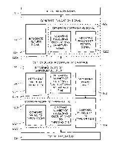
In the following paragraphs, described are exemplary sequences of steps for
detecting
a contactless data storage device 2 within the communication range of the
antenna 4 of
the read/write device 1 with reference to Figure 8. It should be pointed out
that steps
which are arranged in blocks in a common vertical row are performed in the
same
embodiment. For example, steps S1-S21-S311-S331-S4 are associated with the
detection circuit of Figure 6, steps S1-S221-S312-S332-S4 are associated with
the
detection circuit of Figure 1, and steps S1-S222-S32-S34-S4 are associated
with the
detection circuit of Figure 3. Similarly, steps S1-S2-S31-S33-S4 are
associated with the
detection circuits of Figures 1 and 6; whereas steps S1-S22-S3-S4 are
associated with
the detection circuits of Figures 1 and 3.
CA 02754098 2011-09-27
P6332CA00 30
August 2011
18/
In step S1, the detection circuit 10 detects a return signal at the antenna 4
during
emission of an electromagnetic field pulse 30 which is emitted as a short
polling signal.
In step S2, the detection circuit 10 generates an evaluation signal from the
return signal
detected during the transient amplitude build-up [0, ta] of the carrier
oscillation in the
beginning of the electromagnetic field pulse 30. Depending on the embodiment,
the
evaluation signal is generated by integrating the return signal in step S21,
or by
generating a comparative signal in step S22. The comparative signal is
generated to
indicate exceeding oscillations in the return signal, in step S221, or to
indicate the
phasing of the return signal, in step S222.
In step S3, the detection circuit 10 detects a contactless device 2 within the
communication range of the antenna 4 based on the generated evaluation signal.
Depending on the embodiment, the contactless device 2 is detected by
determining, in
step S31, the slope of the amplitude build-up in the transient phase [0, ta]
of carrier
oscillation in the beginning of the electromagnetic field pulse 30, and
comparing, in
step S33, the slope to lower and upper threshold values; or by determining, in
step
S32, the phase shift of the return signal during the amplitude build-up [0,
ta], and
comparing, in step S34, the mean phase shift to lower and upper threshold
values. The
slope of the amplitude build-up is identified by determining, at a defined
point in time,
the value of the integrated return signal, in step S311, or the number of
exceeding
oscillations, in step S312. Correspondingly, the value of the integrated
return signal or
the number of exceeding oscillations are compared to the upper and lower
thresholds,
in step S331 or S332, respectively.
In step S4, the detection circuit 10 defines new upper and lower threshold
values
based on the measurements for the current polling pulse 30, for application in
the
subsequent, next polling pulse 30.
CA 02754098 2011-09-27
P6332CA00 30
August 2011
19/
List of Reference Numerals
1 read/write device (reader)
2 contactless data storage device (contactless device)
3 electromagnetic field (pulse)
=
4 antenna
detection circuit
11 threshold module (Digital/Analog converter)
12 counter
13 processing unit (CPU)
14 timer
input buffer (with hysteresis)
16 Exclusive-Or (XOR) element 16
17 oscillator
18 Analog/Digital converter
antenna coil
magnetic field pulse (polling pulse)
A amplitude of stable oscillation
C, Cl, C2 capacitor
D1, D2 diode
resistor
time
ta amplitude build-up time (rise time)
tm evaluation time (interval)
tp pulse width (length)
Uant antenna voltage
UantCmos phase indicating output signal
Ucomp comparative signal
Ufc carrier frequency signal
UphaseShift phase shift indicating output signal
VC Villard circuit
Vin input reference voltage
Vint slope indicating input voltage
Vthresh threshold voltage
S1-S4 steps