Sélection de la langue

Search

Sommaire du brevet 2771910 

Énoncé de désistement de responsabilité concernant l'information provenant de tiers

Une partie des informations de ce site Web a été fournie par des sources externes. Le gouvernement du Canada n'assume aucune responsabilité concernant la précision, l'actualité ou la fiabilité des informations fournies par les sources externes. Les utilisateurs qui désirent employer cette information devraient consulter directement la source des informations. Le contenu fourni par les sources externes n'est pas assujetti aux exigences sur les langues officielles, la protection des renseignements personnels et l'accessibilité.

Disponibilité de l'Abrégé et des Revendications

L'apparition de différences dans le texte et l'image des Revendications et de l'Abrégé dépend du moment auquel le document est publié. Les textes des Revendications et de l'Abrégé sont affichés :

  • lorsque la demande peut être examinée par le public;
  • lorsque le brevet est émis (délivrance).
(12) Brevet: (11) CA 2771910
(54) Titre français: MODULE DE CELLULE DE CONVERSION, SYSTEME CONVERTISSEUR DE SOURCE DE TENSION COMPRENANT UN TEL MODULE ET PROCEDE DE COMMANDE D'UN TEL SYSTEME
(54) Titre anglais: CONVERTER CELL MODULE, VOLTAGE SOURCE CONVERTER SYSTEM COMPRISING SUCH A MODULE AND A METHOD FOR CONTROLLING SUCH A SYSTEM
Statut: Périmé et au-delà du délai pour l’annulation
Données bibliographiques
Abrégés

Abrégé français

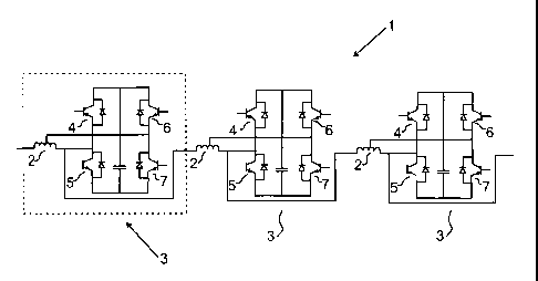
L'invention porte sur un module de cellule de conversion et sur un système convertisseur de source de tension comprenant un tel module. Le module de cellule de conversion comprend au moins deux éléments de commutation, un moyen de stockage d'énergie et un autotransformateur. L'autotransformateur est conçu de façon à court-circuiter le module de cellule de conversion en cas d'apparition d'une défaillance dans ledit module de cellule de conversion.


Abrégé anglais

The invention relates to a converter cell module and a voltage source converter system comprising such a module. The converter cell module comprises at least two switching elements, means for energy storage and an autotransformer. The autotransformer is arranged to bypass the converter cell module in the case of failure occurring in the converter cell module.

Revendications

Note : Les revendications sont présentées dans la langue officielle dans laquelle elles ont été soumises.


9
Claims
1. A single phase converter cell module (3) for a voltage
source converter system (1), which converter cell module (3)
comprises two switching elements, a capacitor (8) and an
autotransformer (2),wherein the switching elements comprise
insulated gate bipolar transistors connected in an H-bridge
configuration having a first and a second terminal,
characterized in that the autotransformer (2) has a first end
terminal, an intermediate terminal, and a second end terminal,
wherein the first and the second terminal of the H-bridge
configuration are connected to the intermediate terminal and
the second end terminal, respectively, wherein the second end
terminal of the autotransformer (2) is an output terminal of
the converter cell module (3) connectable to another converter
cell module, and wherein the first end terminal of the
autotransformer (2) is an input terminal of the converter cell
module (3), whereby the autotransformer (2) bypasses said
converter cell module (3) in the case of failure occurring in
the converter cell module (3).
2. The converter cell module (3) according to claim 1 wherein
said at least two switching elements are connected in parallel
and each having two insulated gate bipolar transistors
connected in series, and each insulated gate bipolar
transistor being connected in anti-parallel with a rectifying
element (9), and wherein capacitor (8) is connected in
parallel with said switching elements.
3. The converter cell module according to claim 1 or 2,
wherein said autotransformer (2) is arranged to provide an
inductance to the converter cell module (3).

10
4. The converter cell module according to any one of claims
1 to 3, further comprising means for electrically
disconnecting the said converter cell module.
5. A voltage source converter system comprising one or
more phases, each of said phases comprising at least two
converter cell modules in accordance with any one of claims
1 to 4 connected in series to each other, wherein the
converter cell modules in the case of failure are arranged to
be bypassed during continuous operation of said system.
6. The converter system according to claim 5, wherein said
system comprises three phases (L1, L2, L3).
7. The converter system according to claim 5 or 6, wherein
said three phases (L1, L2, L3) are connected in a delta
configuration.
8. The converter system according to claim 6, wherein said
three phases (L1, L2, L3) are connected in a Y configuration.
9. Method for controlling a voltage source converter
system according to any of claims 5 to 8, said system
comprising one or 20 more phases, each of said phases
comprising at least two converter cell modules
comprising the step of:
bypassing a converter cell module or modules if a failure
occurs in the said converter cell module or modules.

Description

Note : Les descriptions sont présentées dans la langue officielle dans laquelle elles ont été soumises.


f =
CA 02771910 2012-02-23PCT/EP 2009/061 155- 28-06-2011
EFO
2 8. 06. 2011
05_.)
Converter cell module, voltage source converter system
comprising such a module and a method for controlling such a
system.
Field of the invention
The invention relates to a converter cell module and a
voltage source converter system comprising such a module.
The converter cell module according to the invention
comprises at least two switching elements, means for energy
storage and an autotransformer. The autotransformer is
arranged to bypass the converter cell module in the case of
failure occurring in the converter cell module. The
invention further relates to a method for controlling such a
system.
Background of the invention
Chain-link Multi-level Voltage source converter systems
comprise a number of converter cell modules connected in
series. Each converter cell module forms one "link" (or
cell) of a single phase voltage source converter (VSC) and
is switched on/off a number of times during a fundamental
frequency cycle of an ac system. The chain-link converter
may comprise a number of phases, each phase comprising a
chain of such converter cell modules connected in series to
each other.
Briefly, the converter cell typically comprises
semiconductor assemblies of turn-off type, e.g. insulated
gate bipolar transistors (IGBTs). As an example a converter
cell module comprises four IGBTs. A free-wheeling diode,
also denoted anti-parallel diode, is connected in parallel
with each IGBT and conducts in the opposite direction of the
AMENDED SHEET

CA 02771910 2012-02-23PCT/EP 2009/061 155 - 28-06-2011
2
IGBT. The IGHTs are connected in an H-bridge arrangement
with a DC link capacitor bank.
The number of converter cell modules connected in series for
each phase is proportional to the AC voltage rating of the
ac system. The number of converter cell modules can
therefore be large for high voltage applications having no
mains transformers, which entails high costs. Further, the
current demands on the converter cell modules may also be
low in high voltage systems, resulting in the use of
overrated semiconductor components, which again entails high
costs.
On the other hand, if the application at hand requires
higher currents than available in semiconductor ratings,
converter cells or semiconductor switches have to be
parallel connected, thus yet again resulting in high costs.
In order to provide flexibility in these types of
applications, the use of transformers is a solution.
However, the cost of a mains transformer is high and a mains
transformer requires a large footprint, not available for
all types of applications.
It is necessary that the series connected cells have a
feature that allows the cell to be bypassed in case of a
failure in the cell in order to enable continuous operation
of the converter system without tripping if for example a
semiconductor device fails. That is, if the semiconductor
device, e.g. the IGBT, is damaged the cell cannot be allowed
to go into an open circuit, as the series-connection of
converter cell modules then would form an open circuit.
There are semiconductor devices available that go into short
AMENDED SHEET

CA 02771910 2012-02-23PCT/EP 2009/061 155 - 28-06-201]
3
circuit when damaged, e.g. press-pack IGBTs, which if broken
become a short-circuit, a behaviour that is known as short-
circuit failure mode (SCFM). However, the cost of such
semiconductor devices is very high, even as large as twice
the cost of standard industrial type of devices.
The use of standard industrial type of devices requires the
use of additional components such as very fast bypass
switches that bypass a faulty cell or device. This, yet
again, entails high costs.
US patent having publication number 6,236,580 discloses a
modular multilevel adjustable supply with series connected
active inputs.
The publication "Series 300TM UPS Three Phase 10 kVA to 125
kVA; 60Hz - Installation, Operation & Maintenance Manual" by
Lieber Power Protection discloses a computer protection
system comprising a back-to-back AC converter which can be
bypassed by a switch for maintenance purposes.
"A voltage sag supporter utilizing a PMW-switched
autotransformer", Power Electronics Specialists Conference,
2004, Pesc 04.2004 IEEE 35th annual, Aachen, Germany 20-25
June 2004, Piscataway, JN, USA, IEEE, US vol. 6, 20 June
2004, pp 4244-4250, by Dong-Myung Lee et al. discloses a
distribution-level voltage control scheme that can
compensate voltage sag and swell conditions in three-phase
power systems. Voltage sag support is based on a Pulse Width
Modulated (PWM) autotransformer.
Summary of the invention
AMENDED SHEET

CA 02771910 2016-02-26
4
In view of the above, it is an object of the present invention
to provide an improved topology, and in particular a converter
cell module and a converter system, having a reduced cost
compared to known solutions.
In accordance with the present invention there is provided a
single phase converter cell module for a voltage source
converter system, which converter cell module comprises two
switching elements, a capacitor and an autotransformer,
wherein the switching.elements comprise insulated gate bipolar
transistors connected in an H-bridge configuration having a
first and a second terminal, wherein the autotransformer has
a first end terminal, an intermediate terminal, and a second
end terminal, wherein the first and the second terminal of
the H-bridge configuration are connected to the intermediate
terminal and the second end terminal, respectively, wherein
the second end terminal of the autotransformer is an output
terminal of the converter cell module connectable to another
converter cell module, and wherein the first end terminal of the
autotransformer is an input terminal of the converter cell
module, whereby the 25 autotransformer bypasses said converter
cell module in the case of failure occurring in the converter
cell module.
By such an arrangement the failed module is bypassed
by the autotransformer, in the case of any failure in
the converter cell module, thereby not causing any
operational stop when used in a voltage source
converter system.

CA 02771910 2012-02-23PCT/EP 2009/061 155 - 28-06-201]
In another embodiment wherein said at least two switching
elements are connected in parallel and each having two
insulated gate bipolar transistors connected in series, and
each insulated gate bipolar transistor being connected in
5 anti-parallel with a rectifying element, and wherein said
means for energy storage is connected in parallel with said
switching elements.
In yet another embodiment comprises each of the
semiconductor assemblies an insulated gate bipolar
transistor (IGBT).
In yet another embodiment the autotransformer is arranged to
provide an inductance to the converter cell module.
In yet another embodiment the converter cell module
comprises further means for disconnecting the module.
Thereby can the converter cell module be electrically
disconnected from any other electrical equipment when used
in an electrical system.
In another aspect of the present invention is a voltage
source converter system provided. The system comprises one
or more phases, each of said phases comprising at least two
converter cell modules as claimed in any of claims 1-5.
Bypassing the converter cell modules in the case of failure
is performed during continuous operation of said system.
In another embodiment comprises the system three phases (L1,
L2, L3).
In yet another embodiment are the three phases (L1, L2, L3)
connected in a delta configuration.
AMENDED SHEET

CA 02771910 2012-02-23PCT/EP 2009/061 155 - 28-06-201]
6
Alternatively can the three phases (L1, L2, L3) be connected
in a Y configuration.
In another aspect of the present invention is a method for
controlling a voltage source converter system as claimed in
claims 6-9 provided. The system comprises one or more
phases, each of the phases comprising at least two converter
cell modules. The method comprises bypassing the converter
cell module or modules in which failure has occurred. By
such an arrangement, for example in the case of failure in
any of a plurality of converter cell modules being connected
in series to each other, all of the failed modules are
directly and automatically bypassed by the autotransformer
and the current will flow directly to the next, non-defect
converter cell module. Continuous operation of the converter
system without any operational break is provided even if
several modules fail provided of course that some redundant
cells are available.
Further features and advantages thereof will become clear
upon reading the following detailed description together
with the appended drawings.
Brief description of the drawings
Figure 1 illustrates a converter cell module in accordance
with the present invention.
Figure 2 illustrates a voltage source converter system in
accordance with the present invention.
Figure 3 illustrates the system arranged in a delta
connected arrangement.
AMENDED SHEET

. .
CA 02771910 2012-02-23PCT/EP 2009/061 155 - 28-06-2011
7
Detailed description of embodiments of the invention
Figure 1 illustrates a converter cell module 3 comprising
four IGHT:s (4, 5, 6, 7) connected in a H-bridge
configuration where each semiconductor assembly has a
rectifying element 9 connected in antiparallel. The
converter cell module 3 also comprises a capacitor 8. As
seen in the figure, an autotransformer 2 is connected such
that the converter cell module will be bypassed
automatically in the case of failure in the module. In the
case of failure in any of the IGBT's, current I will flow as
indicated thereby bypassing the module 3.
Figure 2 illustrates a voltage source converter system 1. A
plurality of converter cell modules 3 are connected in
series. If a failure occurs in one, or several of the
converter cell modules 3, that module, or each of those
modules, is/are bypassed by the connection of the
autotransformer(s) 2. After bypassing the defect module, or
modules, the defect module (-s) may be disconnected from the
rest of the converter system by disconnecting means (not
shown). Each of the modules 3 are provided with separate
disconnectors to allow disconnecting of a single module. Due
to the bypassing function provided by the autotransformers
2, no current flows in the defect module (-s) and a cheap
and robust standard disconnector may be used.
Figure 3 illustrates a three phase converter system 1
arranged in a delta connected arrangement. For each phase, a
plurality of converter cell modules 3 are connected in
series to each other. The number of series connected modules
3 depends on the voltage level of the converter system. The
system may also be connected in a Y configuration.
AMENDED SHEET

CA 02771910 2012-02-23PCT/EP 2009/061 155 - 28-06-2011
8
The invention has mainly been described above with reference
to a few embodiments. However, as is readily appreciated by
a person skilled in the art, other embodiments than the ones
disclosed above are equally possible within the scope of the
invention, as defined by the appended patent claims.
AMENDED SHEET

Dessin représentatif
Une figure unique qui représente un dessin illustrant l'invention.
États administratifs

2024-08-01 : Dans le cadre de la transition vers les Brevets de nouvelle génération (BNG), la base de données sur les brevets canadiens (BDBC) contient désormais un Historique d'événement plus détaillé, qui reproduit le Journal des événements de notre nouvelle solution interne.

Veuillez noter que les événements débutant par « Inactive : » se réfèrent à des événements qui ne sont plus utilisés dans notre nouvelle solution interne.

Pour une meilleure compréhension de l'état de la demande ou brevet qui figure sur cette page, la rubrique Mise en garde , et les descriptions de Brevet , Historique d'événement , Taxes périodiques et Historique des paiements devraient être consultées.

Historique d'événement

Description Date
Le délai pour l'annulation est expiré 2019-08-28
Lettre envoyée 2018-08-28
Requête pour le changement d'adresse ou de mode de correspondance reçue 2018-06-11
Lettre envoyée 2017-12-15
Inactive : Transferts multiples 2017-11-30
Accordé par délivrance 2016-07-26
Inactive : Page couverture publiée 2016-07-25
Préoctroi 2016-05-12
Inactive : Taxe finale reçue 2016-05-12
Un avis d'acceptation est envoyé 2016-04-25
Lettre envoyée 2016-04-25
Un avis d'acceptation est envoyé 2016-04-25
Inactive : Approuvée aux fins d'acceptation (AFA) 2016-04-19
Inactive : Q2 réussi 2016-04-19
Modification reçue - modification volontaire 2016-02-26
Inactive : Dem. de l'examinateur par.30(2) Règles 2015-08-26
Inactive : Rapport - Aucun CQ 2015-08-24
Lettre envoyée 2014-06-04
Exigences pour une requête d'examen - jugée conforme 2014-05-14
Toutes les exigences pour l'examen - jugée conforme 2014-05-14
Requête d'examen reçue 2014-05-14
Inactive : Page couverture publiée 2012-05-02
Inactive : CIB en 1re position 2012-04-02
Inactive : Notice - Entrée phase nat. - Pas de RE 2012-04-02
Inactive : CIB attribuée 2012-04-02
Demande reçue - PCT 2012-04-02
Exigences pour l'entrée dans la phase nationale - jugée conforme 2012-02-23
Demande publiée (accessible au public) 2011-03-03

Historique d'abandonnement

Il n'y a pas d'historique d'abandonnement

Taxes périodiques

Le dernier paiement a été reçu le 2016-07-20

Avis : Si le paiement en totalité n'a pas été reçu au plus tard à la date indiquée, une taxe supplémentaire peut être imposée, soit une des taxes suivantes :

  • taxe de rétablissement ;
  • taxe pour paiement en souffrance ; ou
  • taxe additionnelle pour le renversement d'une péremption réputée.

Les taxes sur les brevets sont ajustées au 1er janvier de chaque année. Les montants ci-dessus sont les montants actuels s'ils sont reçus au plus tard le 31 décembre de l'année en cours.
Veuillez vous référer à la page web des taxes sur les brevets de l'OPIC pour voir tous les montants actuels des taxes.

Historique des taxes

Type de taxes Anniversaire Échéance Date payée
Taxe nationale de base - générale 2012-02-23
TM (demande, 2e anniv.) - générale 02 2011-08-29 2012-02-23
TM (demande, 3e anniv.) - générale 03 2012-08-28 2012-07-19
TM (demande, 4e anniv.) - générale 04 2013-08-28 2013-07-12
Requête d'examen - générale 2014-05-14
TM (demande, 5e anniv.) - générale 05 2014-08-28 2014-07-21
TM (demande, 6e anniv.) - générale 06 2015-08-28 2015-07-27
Taxe finale - générale 2016-05-12
TM (demande, 7e anniv.) - générale 07 2016-08-29 2016-07-20
TM (brevet, 8e anniv.) - générale 2017-08-28 2017-08-14
Enregistrement d'un document 2017-11-30
Titulaires au dossier

Les titulaires actuels et antérieures au dossier sont affichés en ordre alphabétique.

Titulaires actuels au dossier
ABB SCHWEIZ AG
Titulaires antérieures au dossier
FALAH HOSINI
JAN SVENSSON
JEAN-PHILIPPE HASLER
Les propriétaires antérieurs qui ne figurent pas dans la liste des « Propriétaires au dossier » apparaîtront dans d'autres documents au dossier.
Documents

Pour visionner les fichiers sélectionnés, entrer le code reCAPTCHA :


Pour visualiser une image, cliquer sur un lien dans la colonne description du document. Pour télécharger l'image (les images), cliquer l'une ou plusieurs cases à cocher dans la première colonne et ensuite cliquer sur le bouton "Télécharger sélection en format PDF (archive Zip)" ou le bouton "Télécharger sélection (en un fichier PDF fusionné)".

Liste des documents de brevet publiés et non publiés sur la BDBC .

Si vous avez des difficultés à accéder au contenu, veuillez communiquer avec le Centre de services à la clientèle au 1-866-997-1936, ou envoyer un courriel au Centre de service à la clientèle de l'OPIC.


Description du
Document 
Date
(aaaa-mm-jj) 
Nombre de pages   Taille de l'image (Ko) 
Description 2012-02-22 8 294
Dessin représentatif 2012-02-22 1 6
Dessins 2012-02-22 2 32
Revendications 2012-02-22 2 78
Abrégé 2012-02-22 1 56
Description 2016-02-25 8 284
Revendications 2016-02-25 2 73
Dessin représentatif 2016-06-01 1 6
Avis d'entree dans la phase nationale 2012-04-01 1 194
Rappel - requête d'examen 2014-04-28 1 116
Accusé de réception de la requête d'examen 2014-06-03 1 175
Avis du commissaire - Demande jugée acceptable 2016-04-24 1 161
Avis concernant la taxe de maintien 2018-10-08 1 180
PCT 2012-02-22 22 784
PCT 2012-02-23 7 311
Demande de l'examinateur 2015-08-25 3 204
Modification / réponse à un rapport 2016-02-25 4 129
Taxe finale 2016-05-11 2 47