Note : Les descriptions sont présentées dans la langue officielle dans laquelle elles ont été soumises.
CA 02780359 2012-06-20
111262:910654
DESCRIPTION
TITLE OF INVENTION
Method of Manufacturing Silicon Carbide Semiconductor Device
TECHNICAL FIELD
The present invention relates to a method of manufacturing a silicon carbide
semiconductor device.
BACKGROUND ART
In manufacturing a semiconductor device, the step of selectively forming an
impurity region in a semiconductor substrate is required. For example, in
manufacturing an n-channel type MOSFET (Metal Oxide Semiconductor Field Effect
Transistor), in order to obtain an npn structure, the step of partially
forming a p-type
impurity region in an n-type semiconductor substrate and further partially
forming an n-
type impurity region in this p-type impurity region is often performed.
Namely, two
impurity regions different in extension from each other are formed. In a case
where a
silicon substrate is employed, since extension of an impurity region can be
adjusted by
diffusion, a double diffusion technique utilizing this feature has widely been
used.
Meanwhile, in a case where a silicon carbide substrate is employed, a
diffusion
coefficient of an impurity is small and hence it is difficult to adjust
extension of an
impurity region by diffusion. Namely, a region into which ions have been
implanted
becomes an impurity region substantially as it is through activation
annealing.
Therefore, the double diffusion technique cannot be employed. Thus, for
example
according to Japanese Patent Laying-Open No. 6-151860 (PTL 1), ions are
implanted
by using a gate electrode having an inclined surface at an end surface as a
mask. By
utilizing the fact that a range of impurity ions in ion implantation can be
controlled by
an acceleration voltage, a desired impurity region is formed.
CITATION LIST
PATENT LITERATURE
-1-
CA 02780359 2012-06-20
111262:910654
PTL 1: Japanese Patent Laying-Open No. 6-151860
SUMMARY OF INVENTION
TECHNICAL PROBLEM
In the method above, extension of an impurity region is largely dependent on
accuracy in formation of an inclined surface of a gate electrode, and hence
error in
extension of the impurity becomes great.
The present invention was made in view of the problems above, and an object of
the present invention is to provide a method of manufacturing a silicon
carbide
semiconductor device capable of enhancing accuracy in extension of an impurity
region.
SOLUTION TO PROBLEM
According to a method of manufacturing a silicon carbide semiconductor device
of the present invention, the following steps are performed.
A silicon carbide substrate having a surface is prepared. An etching stop
layer
is formed on the surface of the silicon carbide substrate. A mask layer is
deposited on
the etching stop layer. In the mask layer, a first opening surrounded by a
first sidewall
is formed. A first impurity region having a first conductivity type is formed
from the
surface to a first depth in the silicon carbide substrate by ion implantation
through the
first opening. After the step of forming a first impurity region, by
depositing a spacer
layer on the etching stop layer on which the mask has been provided, a mask
portion
having the mask layer and the spacer layer is formed. The spacer layer covers
the first
sidewall and the etching stop layer in the first opening. By anisotropically
etching the
spacer layer in the first opening, a second opening surrounded by a second
sidewall is
formed in the mask portion. A second impurity region having a second
conductivity
type different from the first conductivity type is formed from the surface to
a second
depth smaller than the first depth in the silicon carbide substrate, by ion
implantation
through the second opening. An angle of the second sidewall with respect to
the
surface is 90 10 across a height as great as the second depth. It is noted
that
"90 10 " means 80 or greater and 100 or smaller.
-2-
CA 02780359 2012-06-20
111262: 910654
According to the manufacturing method above, an angle of the second sidewall
of the mask portion with respect to the surface of the silicon carbide
substrate is
90 10 , that is, substantially perpendicular, across the height as great as
the second
depth of the second impurity region. Thus, in ion implantation for forming the
second
impurity region, substantially no region where the mask portion has a small
thickness
due to inclination of the second sidewall exists in the vicinity of the second
sidewall.
Therefore, introduction of ions into the silicon carbide substrate through the
mask
portion in the vicinity of the second sidewall can be suppressed. Thus,
substantially
no impurity region can be formed in a portion covered with the mask portion.
Therefore, accuracy in extension of the second impurity region can be
enhanced.
Preferably, the mask portion is removed after the second impurity region is
formed. Thus, the portion covered with the mask portion in the silicon carbide
substrate can be exposed. Further, preferably, a gate insulating film and a
gate
electrode are formed on the silicon carbide substrate after the mask portion
is removed.
Thus, a gate insulating film and a gate electrode free from change in quality
due to
exposure to ion implantation for forming the first and second impurity regions
can be
formed.
Preferably, an angle of the first sidewall with respect to the surface is 90
10
across a height as great as the first depth. Thus, in ion implantation for
forming the
first impurity region, substantially no region where the mask portion has a
small
thickness due to inclination of the first sidewall exists in the vicinity of
the first
sidewall. Therefore, introduction of ions into the silicon carbide substrate
through the
mask portion in the vicinity of the first sidewall can be suppressed. Thus,
substantially no impurity region can be formed in a portion covered with the
mask
portion. Therefore, accuracy in extension of the first impurity region can be
enhanced.
Preferably, an ion implantation angle in the step of forming a second impurity
region is not smaller than 0 and not greater than 6 . Namely, ions are
implanted
substantially perpendicularly to the surface of the silicon carbide substrate.
Thus, as
CA 02780359 2012-06-20
111262:910654
compared with a case where an ion implantation angle is greater, introduction
of ions
into the silicon carbide substrate through the mask portion in the vicinity of
the second
sidewall can further be suppressed.
Preferably, the second sidewall includes a portion of which angle with respect
to
the surface of the silicon carbide substrate is 90 l 0 and a height of this
portion is not
smaller than 0.5 m and not greater than 2.5 m. As this height is not smaller
than 0.5
m, introduction of ions into the silicon carbide substrate through the mask
portion can
further be suppressed. As this height is not greater than 2.5 m, a thinner
mask
portion can be used and hence warpage of the silicon carbide substrate due to
stress in
the mask portion can be suppressed.
An ion implantation angle in the step of forming a second impurity region may
be not smaller than 3 and not greater than 6 , and a surface of the silicon
carbide
substrate may be a (0-33-8) plane of a hexagonal crystal. As the surface of
the silicon
carbide substrate is the (0-33-8) plane of a hexagonal crystal, channel
mobility of
carriers at the surface can be enhanced. In addition, as the ion implantation
angle is
not smaller than 3 , channeling of implanted ions in the silicon carbide
substrate can be
suppressed.
An ion implantation angle in the step of forming a second impurity region may
be 0 , and a surface of the silicon carbide substrate may be inclined by 3 or
more from
a {0001 } plane of a hexagonal crystal in order to prevent a channeling
phenomenon
during ion implantation. As the ion implantation angle is 0 , introduction of
ions into
the silicon carbide substrate through the mask portion in the vicinity of the
second
sidewall can further be suppressed.
Preferably, the mask layer is made of any of silicon oxide and polysilicon.
Preferably, the spacer layer is made of any of silicon oxide and polysilicon.
Preferably, a material for the etching etching stop layer is different from a
material for the mask layer. Further preferably, the etching stop layer
includes at least
any of a silicon nitride layer, a polysilicon layer, a silicon oxide layer. a
silicon
-4-
CA 02780359 2012-06-20
111262:910654
oxynitride layer, and a titanium layer. Further preferably, the etching stop
layer has a
thickness not smaller than 10 nm and not greater than 500 nm. In a case where
the
etching stop layer includes a. titanium layer, preferably, an underlying layer
made of any
of silicon oxide and polysilicon is provided between the titanium layer
serving as the
etching stop layer and the silicon carbide substrate.
ADVANTAGEOUS EFFECTS OF INVENTION
As is clear from the description above, according to the present invention.
accuracy in extension of an impurity region can be enhanced.
BRIEF DESCRIPTION OF DRAWINGS
Fig. 1 is a partial cross-sectional view schematically showing a construction
of a
silicon carbide semiconductor device in a first embodiment of the present
invention.
Fig. 2 is a partial cross-sectional view schematically showing a first step in
a
method of manufacturing a silicon carbide semiconductor device in Fig. 1.
Fig. 3 is a partial cross-sectional view schematically showing a second step
in
the method of manufacturing a silicon carbide semiconductor device in Fig. 1.
Fig. 4 is a partial cross-sectional view schematically showing a third step in
the
method of manufacturing a silicon carbide semiconductor device in Fig. 1.
Fig. 5 is a partial cross-sectional view schematically showing a fourth step
in the
method of manufacturing a silicon carbide semiconductor device in Fig. 1.
Fig. 6 is a partial cross-sectional view schematically showing a fifth step in
the
method of manufacturing a silicon carbide semiconductor device in Fig. 1.
Fig. 7 is a partial cross-sectional view schematically showing a sixth step in
the
method of manufacturing a silicon carbide semiconductor device in Fig. 1.
Fig. 8 is a partial cross-sectional view schematically showing a seventh step
in
the method of manufacturing a silicon carbide semiconductor device in Fig. 1.
Fig. 9 is a partial cross-sectional view schematically showing an eighth step
in
the method of manufacturing a silicon carbide semiconductor device in Fig. 1.
Fig. 10 is a. partial cross-sectional view schematically showing a ninth step
in
-5-
CA 02780359 2012-06-20
111262: 910654
the method of manufacturing a silicon carbide semiconductor device in Fig. 1.
Fig. 11 is a partial cross-sectional view schematically showing a tenth step
in
the method of manufacturing a silicon carbide semiconductor device in Fig. 1.
Fig. 12 is a partial cross-sectional view schematically showing an eleventh
step
in the method of manufacturing a silicon carbide semiconductor device in Fig.
1.
Fig. 13 is a partial cross-sectional view schematically showing a twelfth step
in
the method of manufacturing a silicon carbide semiconductor device in Fig. 1.
Fig. 14 is a partial cross-sectional view schematically showing a thirteenth
step
in the method of manufacturing a silicon carbide semiconductor device in Fig.
1.
Fig. 15 is a partial cross-sectional view schematically showing a fourteenth
step
in the method of manufacturing a silicon carbide semiconductor device in Fig.
1.
Fig. 16 is a partially enlarged view of Fig. 12.
Fig. 17 is a partial cross-sectional view schematically showing a variation of
the
step in Fig. 3.
Fig. 18 is a partial cross-sectional view schematically showing a construction
of
a silicon carbide semiconductor device in a second embodiment of the present
invention.
Fig. 19 is a partial cross-sectional view schematically showing a first step
in a
method of manufacturing a silicon carbide semiconductor device in the second
embodiment of the present invention.
Fig. 20 is a partial cross-sectional view schematically showing a second step
in
the method of manufacturing a silicon carbide semiconductor device in the
second
embodiment of the present invention.
Fig. 21 is a partial cross-sectional view schematically showing a third step
in the
method of manufacturing a silicon carbide semiconductor device in the second
embodiment of the present invention.
Fig. 22 is a partial cross-sectional view schematically showing a construction
of
a silicon carbide semiconductor device in a third embodiment of the present
invention.
-6-
CA 02780359 2012-06-20
111262:910654
Fig. 23 is a partial cross-sectional view schematically showing a thirteenth
step
in the method of manufacturing a silicon carbide semiconductor device in Fig.
22.
Fig. 24 is a partial cross-sectional view schematically showing a fourteenth
step
in the method of manufacturing a silicon carbide semiconductor device in Fig.
22.
Fig. 25 is a partial cross-sectional view schematically showing a fifteenth
step in
the method of manufacturing a silicon carbide semiconductor device in Fig. 22.
Fig. 26 is a partial cross-sectional view schematically showing a sixteenth
step
in the method of manufacturing a silicon carbide semiconductor device in Fig.
22.
Fig. 27 is a partial cross-sectional view schematically showing a seventeenth
step in the method of manufacturing a silicon carbide semiconductor device in
Fig. 22.
Fig. 28 is a partial cross-sectional view schematically showing an eighteenth
step in the method of manufacturing a silicon carbide semiconductor device in
Fig. 22.
DESCRIPTION OF EMBODIMENTS
An embodiment of the present invention will be described hereinafter with
reference to the drawings.
(First Embodiment)
As shown in Fig. 1, a silicon carbide semiconductor device in the present
embodiment is a MOSFET 100, and it is specifically a vertical DiMOSFET (Double
Implanted MOSFET). MOSFET 100 has an epitaxial substrate 90, an oxide film
126,
a source electrode 111, an upper source electrode 127, a gate electrode 1 10.
and a drain
electrode 112. Epitaxial substrate 90 has a single crystal substrate 80, a
buffer layer
121, a breakdown voltage holding laver 122, a p region 123, and an n+ region
124. A.
two-dimensional shape (a shape when viewed from above in Fig. 1) of MOSFET 100
is
for example, a rectangle or a square having a side of a length not shorter
than 2 mm.
Single crystal substrate 80 and buffer layer 121 each have an n conductivity
type.
Single crystal substrate 80 is preferably composed of silicon carbide.
Concentration of
an n-type conductive impurity in buffer layer 121 is, for example, 5x10¹⁷ CM-3
. In
addition, buffer layer 121 has a thickness. for example, of 0.5 m.
-7-
CA 02780359 2012-06-20
111262:910654
Breakdown voltage holding laver 122 is formed on buffer layer 121, and it is
composed of silicon carbide having an n conductivity type. For example,
breakdown
voltage holding layer 122 has a thickness of 10 pm and concentration of an n-
type
conductive impurity is 5 x 1015 cm 3.
On a surface SO of epitaxial substrate 90, a plurality of p regions 123 having
a p
conductivity type are formed at a distance from one another. In addition, in
surface
SO, n+ region 124 is formed to be located inside each p region 123. In surface
SO, p
region 123 has a channel region lying between n+ region 124 and breakdown
voltage
holding layer 122 and covered with gate electrode l 10 with oxide film 126
being
interposed. The channel region has a channel length CL.
On breakdown voltage holding layer 122 exposed between the plurality of p
regions 123 at surface SO, oxide film 126 is formed. Specifically, oxide film
126 is
formed to extend from n+ region 124 in one p region 123 to p region 123,
breakdown
voltage holding laver 122 exposed between two p regions 123, the other p
region 123,
and n+ region 124 in the other p region 123. Gate electrode 110 is formed on
oxide
film 126. Therefore, a portion of oxide film 126 having gate electrode 110
formed
thereon has a function as a gate insulating film. In addition, source
electrode 111 is
formed on n- region 124. A part of source electrode 11 l may be in contact
with p
region 123. Upper source electrode 127 is formed on source electrode 111.
A method of manufacturing MOSFET 100 will now be described.
As shown in Fig. 2, epitaxial substrate 90 (silicon carbide substrate) having
surface SO is prepared. Specifically, buffer layer 121 is formed on a main
surface of
single crystal substrate 80. and breakdown voltage holding layer 1.22 is
formed on
buffer layer 121. Buffer laver 121 is composed of silicon carbide having an n
conductivity type, and it has a thickness, for example, of 0.5 m. In
addition,
concentration of the conductive impurity in buffer layer 121 is set, for
example, to
5x1017 cm-3. Breakdown voltage holding layer 122 has a thickness, for example,
of
10 m. Further, concentration of then conductive impurity in breakdown voltage
-8-
CA 02780359 2012-06-20
111262 : 910654
holding layer 122 is set, for example, to 5x 1015 cm 3.
As shown in Fig. 3, an etching stop layer 50 is formed on surface SO of
epitaxial substrate 90. Preferably, a material for etching stop layer 50 is
different from
a material for a mask layer 31 (Fig. 4) which will be described later.
Preferably,
etching stop layer 50 is a silicon nitride layer or a titanium layer. The
titanium layer
has a thickness, for example, not smaller than 50 nm and not greater than 200
nm.
As shown in Fig. 4, mask layer 31 is deposited on etching stop layer 50.
Preferably, mask layer 31 is made of any of silicon oxide and polysilicon.
As shown in Fig. 5, a photoresist pattern 40 is formed on mask layer 31.
As shown in Fig. 6, mask layer 3 1 is patterned through anisotropic etching E1
using photoresist pattern 40 as a mask. Remaining photoresist pattern 40 is
removed.
As shown in Fig. 7, as a result of etching above, an opening P 1 (a first
opening)
surrounded by a sidewall S I (a first sidewall) is formed in mask layer 31.
As shown in Fig. 8, as a result of ion implantation JI through opening P1, p
region 123 (a first impurity region) having p-type (the first conductivity
type) is formed
from surface SO to a depth D 1 (a first depth) in epitaxial substrate 90.
As shown in Fig. 9, thereafter by depositing a spacer layer 32 on etching stop
layer 50 on which mask layer 31 has been provided, a mask portion 30 having
mask
layer 31 and spacer layer 32 is formed. Spacer layer 32 covers sidewall S 1
and
etching stop layer 50 in opening P l. Preferably, spacer layer 32 is made of
any of
silicon oxide and polysilicon.
As shown in Fig. 10. spacer layer 32 in opening P1 is patterned by anisotropic
etching E2.
As shown in Fig. 11, an opening P2 (a second opening) surrounded by a
sidewall S2 (a second sidewall) is thus formed in mask portion 30.
As shown in Fig. 12. as a result of ion implantation J2 through opening P2, n+
region 124 (a second impurity region) having n-type (the second conductivity
type) is
formed from surface SO to a depth D2 (a second depth) smaller than depth DI in
-9-
CA 02780359 2012-06-20
111262:910654
epitaxial substrate 90. As shown in Fig. 16 in further detail, an angle AW of
an entire
portion S2L of sidewall S2 (Fig. 11) across a height HT with respect to
surface SO is
90 10 and preferably 90 5 . Height HT is equal to or greater than depth D2.
As described above, sidewall S2 includes a portion of which angle AW with
respect to surface SO is 90 10 . The height of this portion is preferably not
smaller
than 0.5 m and not greater than 2.5 m.
In addition, in a case where sidewall S2 includes a portion of which angle AW
with respect to surface SO is 90 5 , the height of this portion is preferably
not smaller
than 0.5 pm and not greater than 2.5 m.
Preferably, an angle of sidewall S 1 (Fig. 7) with respect to surface SO is
90 10 and preferably 90 5 across a height as great as depth Dl (Fig. 8).
Preferably, as shown in Fig. 16, an angle between a direction of travel IL of
ion
beams during ion implantation J2 (Fig. 12) and a normal NL of surface SO, that
is, an
ion implantation angle Al, is not smaller than 0 and not greater than 6 . Ion
implantation angle Al in the step of forming nT region 124 may be not smaller
than 3
and not greater than 6 and surface SO of epitaxial substrate 90 may be a (0-
33-8) plane
of a hexagonal crystal. In addition, ion implantation angle Al in the step of
forming n
region 124 may be 0 and surface SO of epitaxial substrate 90 may be inclined
by an
angle not smaller than 3 and not greater than 6 from a {0001 } plane of a
hexagonal
crystal in order to prevent a channeling phenomenon during ion implantation.
As further shown in Fig. 13, thereafter. mask portion 30 and etching stop
laver
50 are removed. In addition, activation annealing treatment is performed. For
example, annealing for 30 minutes at a heating temperature of 1700 C in an
argon
atmosphere is performed.
As shown in Fig. 14. oxide film 126 having a function as a gate insulating
film
is formed on epitaxial substrate 90. Specifically, oxide film 126 is formed to
cover
breakdown voltage holding layer 122, p region 123, and n+ region 124.
Formation
may be carried out by dry oxidation (thermal oxidation). Conditions in dry
oxidation
-10-
CA 02780359 2012-06-20
111262:910654
are, for example, a heating temperature of 1200 C and a heating time period of
30
minutes.
Thereafter, a nitriding annealing step is performed. Specifically, annealing
treatment in a nitrogen monoxide (NO) atmosphere is performed. Conditions in
this
treatment are, for example, a heating temperature of 1100 C and a heating time
period
of 120 minutes. Consequently, nitrogen atoms are introduced in the vicinity of
an
interface between each of breakdown voltage holding layer 122, p region 123)
and n-
region 124 and oxide film 126. It is noted that, after this annealing step
using nitrogen
monoxide, annealing treatment using an argon (Ar) gas which is an inert gas
may
further be performed. Conditions in this treatment are, for example, a heating
temperature of 1100 C and a heating time period of 60 minutes.
As shown in Fig. 15, source electrode 11 1 is formed as follows.
A resist film having a pattern is formed on oxide film 126 with
photolithography. Using this resist film as a mask, a portion of oxide film
126 located
on n+ region 124 is etched away. Thus, an opening is formed in oxide film 126.
Then, a conductor film is formed in this opening to be in contact with n
region 124.
Then, by removing the resist film, a portion of the conductor film above that
has been
located on the resist film is removed (lift-off). This conductor film may be a
metal
film and it is composed, for example, of nickel (Ni). As a result of this lift-
off, source
electrode 111 is formed.
It is noted that heat treatment for alloying is preferably performed here. For
example, heat treatment for 2 minutes at a heating temperature of 950 C in an
atmosphere of an argon (Ar) gas which is an inert gas is performed.
Referring again to Fig. 1, upper source electrode 127 is formed on source
electrode 111. In addition, gate electrode 110 is formed on oxide film 126.
Moreover, drain electrode 1 12 is formed on a back surface (a lower surface in
the
drawing) of single crystal substrate 80.
MOSFET 100 (Fig. 1) is obtained as described above.
-11-
CA 02780359 2012-06-20
111262:91064
According to the present embodiment, as shown in Fig. 16, angle AW of
sidewall S2 (Fig. 11) of mask portion 30 with respect to surface SO of
epitaxial
substrate 90 is 90 10 across height HT as great as depth D2 of n` region
124. Thus,
during ion implantation for forming n+ region 124, substantially no region
where mask
portion 30 has a small thickness due to inclination of sidewall S2 exists in
the vicinity
of sidewall S2. Therefore, introduction of ions into epitaxial substrate 90
through
mask portion 30 in the vicinity of sidewall S2 can be suppressed. Thus,
substantially
no n+ region 124 can be formed in a portion covered with mask portion 30.
Therefore,
accuracy in extension of n+ region 124 can be enhanced. In particular,
accuracy in
channel length CL (Fig. 1) can be enhanced.
Preferably, mask portion 30 is removed after n+ region 124 is formed. Thus, a
portion of epitaxial substrate 90 that has been covered with mask portion 30
can be
exposed. Further preferably, after mask portion 30 is removed, oxide film 126
(a gate
insulating film) and gate electrode 110 are formed on epitaxial substrate 90.
Thus, a
gate insulating film and a gate electrode free from change in quality due to
exposure to
ion implantation for forming p region 123 and n+ region 124 can be formed.
Preferably, an angle of sidewall Si (Fig. 7) with respect to surface SO is
90 10 across the height as great as depth Dl. Thus, during ion implantation
for
forming p region 123, substantially no region where mask portion 30 has a
small
thickness due to inclination of sidewall S I exists in the vicinity of
sidewall S 1.
Therefore, introduction of ions into epitaxial substrate 90 through mask
portion 30 in
the vicinity of .si dewal_l S 1 can be suppressed. Thus, substantially no p
region 123 can
be formed in the portion covered with mask portion 30. Therefore, accuracy in
extension of p region 123 can be enhanced.
Preferably, as shown in Fig. 16, ion implantation angle Al in the step of
forming
n+ region 124 is not smaller than 0 and not greater than 6 . Thus, as
compared with a
case where an ion implantation angle is greater, introduction of ions into
epitaxial
substrate 90 through mask portion 30 in the vicinity of sidewall S2 (Fig. 11)
can further
-12-
CA 02780359 2012-06-20
111262:910654
be suppressed.
Preferably, as shown in Fig. 16, sidewall S2 (Fig. 11) includes a portion of
which angle AW with respect to surface SO of epitaxial substrate 90 is 90 10
and a
height of this portion is not smaller than 0.5 m and not greater than 2.5 m.
As this
height is not smaller than 0.5 m, introduction of ions into epitaxial
substrate 90
through mask portion 30 can further be suppressed. As this height is not
greater than
2.5 m, warpage of the silicon carbide substrate due to stress in mask portion
30 can be
suppressed.
Ion implantation angle Al (Fig. 16) in the step of forming n+ region 124 may
be
not smaller than 3 and not greater than 6 . and surface SO of epitaxial
substrate 90
maybe a (0-33-8) plane of a hexagonal crystal. As surface SO of epitaxial
substrate
90 is the (0-33-8) plane of a hexagonal crystal, channel mobility of carriers
at surface
SO can be enhanced. In addition, as ion implantation angle Al is not smaller
than 3 ,
channeling of implanted ions in epitaxial substrate 90 can be suppressed.
Ion implantation angle Al (Fig. 16) in the step of forming n+ region 124 may
be
0 , and surface SO of epitaxial substrate 90 may be inclined by 3 or more
from a
{0001 } plane of a hexagonal crystal in order to prevent a channeling
phenomenon
during ion implantation. As ion implantation angle Al is 0 , introduction of
ions into
epitaxial substrate 90 through mask portion 30 in the vicinity of sidewall S2
can further
be suppressed.
As a variation of the step in Fig. 3, an underlying layer 51 (Fig. 17) made of
any
of silicon oxide and polysilicon may be provided between a titanium layer
serving as
etching stop layer 50 and epitaxial substrate 90. Underlying layer 51 can
prevent
contamination of epitaxial substrate 90 by the titanium layer, that is, the
metal layer.
Though a silicon nitride layer or a titanium layer is exemplified as the
etching
stop layer in the present embodiment, the construction of the etching stop
layer is not
limited thereto. The etching stop layer may be, for example, any of a silicon
nitride
layer, a polysilicon layer. a silicon oxide layer. a silicon oxynitride layer,
and a titanium
-13-
CA 02780359 2012-06-20
111262 : 910654
laver, or a laver made of a stack including at least any of these layers, or a
laver made of
a stack including two or more of these layers. A lower limit of a thickness of
the
etching stop layer is preferably 10 nm, more preferably 30 nm, and further
preferably 50
nm. Meanwhile, an upper limit of a thickness of the etching stop layer is
preferably
500 nm, more preferably 400 nm, and further preferably 300 nm.
(Second Embodiment)
As shown in Fig. 18, a silicon carbide semiconductor device in the present
embodiment is a MOSFET 200 and specifically a vertical DiMOSFET. MOSFET 200
has an n+ region 124a and an n+ region 124b instead of n region 124 (Fig. 1).
N~
region 124a and n+ region 124b are arranged in surface SO at a distance from
each other.
P region 123 between n+ region 124a and n+ region 124b reaches surface SO and
is in
contact with source electrode 111.
A method of manufacturing MOSFET 200 will now be described. It is noted
that the process is similarly performed also in the present embodiment until
the step in
Fig. 9 in the manufacturing method in the first embodiment.
As shown in Fig. 19, in opening P1, a photoresist pattern 41 is formed on
spacer
layer 32 so as to be arranged at a distance from sidewall S 1.
As shown in Fig. 20, spacer layer 32 in opening PI is patterned by anisotropic
etching E2, using photoresist pattern 41 as a mask. Remaining photoresist
pattern 41
is removed.
As shown in Fig. 21, as a result of ion implantation J2 through a portion of
opening P2 from which spacer laver 32 has been removed, n+ regions (the second
impurity regions) 124a and 124b having n-type (the second conductivity type)
are
formed. It is noted that each of n+ regions 124a and 124b has a depth equal to
depth
D2 of n+ region 124 (Fig. 16), and in the present embodiment as well, during
ion
implantation J2, sidewall S2 has portion S2L (Fig. 16) as in the first
embodiment.
Since the construction other than the above is substantially the same as in
the
first embodiment described above. the same or corresponding elements have the
same
-14-
CA 02780359 2012-06-20
111262:910654
reference characters allotted and description thereof will not be repeated.
According to the present embodiment, as shown in Fig. 18, p region 123
between n+ region 124a and n` region 124b reaches surface SO and is in contact
with
source electrode 111. According to this construction, a potential of p region
123 is
stabilized.
In addition, a mask for isolating n+ region 124a and n+ region 124b is formed
independently of patterning (Fig. 6) of mask layer 31. Therefore, difficulty
in
patterning of mask layer 31 does not become high.
(Third Embodiment)
As shown in Fig. 22, epitaxial substrate 90 in a MOSFET 300 in the present
embodiment has a p+ region 125 (a third impurity region). P_ region 125
connects
surface SO and p region 123 to each other. In addition, p+ region 125 is
higher in
impurity concentration than p region 123. Preferably, p region 125 is formed
to
penetrate n- region 124 to reach p region 123. Source electrode 111 is formed
on ny
region 124 and p+ region 125.
As in the first embodiment, in surface SO, p region 123 forms a channel region
having channel length CL. Channel length CL is preferably not. smaller than
0.1 pm
and not greater than 1.5 m.
A method of manufacturing MOSFET 300 will now be described. Since the
former part of the manufacturing method is substantially the same as the first
to twelfth
steps (Figs. 2 to 13) in the first embodiment, description thereof will not be
provided.
As shown in Fig. 23, an etching stop layer 50a is formed on surface SO.
Etching stop layer 50a is formed similarly to etching stop layer 50 described
above.
Then, a mask layer 31a is formed on etching stop layer 50a. Mask layer 31 a
can be
formed similarly to mask layer 31 described above.
As shown in Fig. 24, an opening is formed in mask layer 31a. This opening
exposes a part of etching stop layer 50a in two-dimensional view (a field of
view from
above in Fig. 24). A portion of etching stop layer 50a exposed through this
opening is
- 15 -
CA 02780359 2012-06-20
111262:910654
surrounded by a portion not exposed through this opening. Then, ion
implantation J3
into epitaxial substrate 90 through this opening is performed.
As shown in Fig. 25, as a result of ion implantation above, p+ region 125 is
formed in epitaxial substrate 90.
As shown in Fig. 26, thereafter, mask layer 31 a and etching stop layer 50a
are
removed. In addition, activation annealing treatment is performed. For
example,
annealing for 30 minutes at a heating temperature of 1700 C in an argon
atmosphere is
performed. It is noted that annealing in the step in Fig. 13 can be omitted by
performing this annealing step.
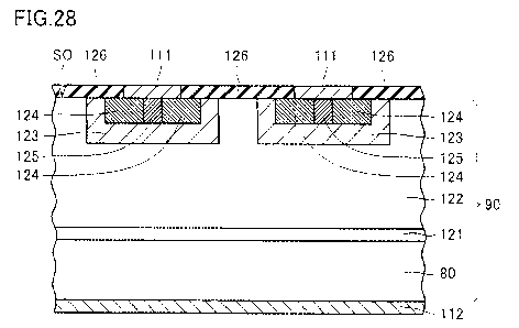
As shown in each of Figs. 27 and 28, the steps substantially the same as the
steps in Figs. 14 and 15 are performed.
MOSFET 300 (Fig. 22) is obtained as described above.
According to the present embodiment, as p region 123 is connected to source
electrode 111 through p+ region 125, a potential of p region. 123 is
stabilized.
Though the steps substantially the same as the steps in Figs. 2 to 13 in the
first
embodiment are performed in the former part of the manufacturing method in the
present embodiment, steps substantially the same as the steps in Figs. 19 to
21 in the
second embodiment may be performed instead. In this case, p+ region 125 may be
formed between n+ regions 124a and 124b (Fig. 21).
In each embodiment above, p-type and n-type may be interchanged. In
addition, in each embodiment above, though epitaxial substrate 90 is employed
as the
silicon carbide substrate, a silicon carbide single crystal substrate may be
employed
instead.
It should be understood that the embodiments disclosed herein are illustrative
and non-restrictive in every respect. The scope of the present invention is
defined by
the terms of the claims, rather than the description above, and is intended to
include any
modifications within the scope and meaning equivalent to the terms of the
claims.
REFERENCE SIGNS LIST
-16-
CA 02780359 2012-06-20
111262:910654
30 mask portion; 31, 31 a mask layer; 32 spacer layer; 40, 41 photoresist
pattern;
50, 50a etching stop layer; 51 underlying layer; 80 single crystal substrate;
90 epitaxial
substrate (silicon carbide substrate); 100, 200, 300 MOSFET (silicon carbide
semiconductor device); 110 gate electrode; 111 source electrode; 112 drain
electrode;
121 buffer layer; 122 breakdown voltage holding layer; 123 p region (first
impurity
region); 124, 124a, 124b n+ region (second impurity region); 125 p region; 126
oxide
film; 127 upper source electrode; AW angle; P1 opening (first opening); P2
opening
(second opening); SO surface; S 1 sidewall (first sidewall); and S2 sidewall
(second
sidewall).
-17-