Note : Les descriptions sont présentées dans la langue officielle dans laquelle elles ont été soumises.
CA 02818087 2013-05-15
Doc. No.: 152-5 CA/PCT
Patent
PROCESS FOR MAKING A HEAT RADIATING STRUCTURE FOR HIGH-POWER
LED
FIELD OF THE INVENTION
The present invention relates to a technology of making a heat radiating
device, more
particularly, to a process of making a heat radiating structure for high-power
LED.
BACKGROUND OF THE INVENTION
LED has been widely used in many applications such as indicative marks
application and
indoor/outdoor lighting application, due to its long theoretical lifetime, low
energy consumption,
eco-friendly characteristic and the like. As we all know, the most crucial
factor affecting the
lifetime of LED is LED's heat radiation, and this is especially true for high-
power LED. Existing
method of making a heat radiating structure for high-power LED mainly includes
successively
connecting a heat sink, an aluminum substrate, a heat conductive silicone
grease, a heat radiating
plate and other parts together, the LED thus connects with the aluminum
substrate through the
heat sink, this is a simple method, however, the resulting heat radiating
structure has poor
performance in thermal conduction and radiation, which is largely ascribed to
the structural
setting of the aluminum substrate, this poor performance hence greatly affects
the application
field as well as the application range of the LED. The aluminum substrate is
usually formed by
successively superposing a protective oil layer, a copper foil layer, an
insulating layer and an
aluminum plate layer, whilst the insulating layer plays a positive role in
electric insulation, it
plays a role in thermal insulation which is not expected, hence heat produced
by the LED cannot
be removed timely, which finally largely affects the lifetime of the LED.
Consequently,
technological innovations should be made in the field of making heat radiating
structures for
LED to realize differentiated heat radiating structures and to solve the
problem of heat radiation
of the LED.
SUMMARY OF THE INVENTION
The object of the present invention is to provided a process of making a heat
radiating
structure for high-power LED with simple process and high production
efficiency so as to
1
CA 02818087 2013-05-15
Doc. No.: 152-5 CA/PCT
Patent
overcome the above shortcomings in the prior arts, and the resulting heat
radiating structure
made by this process has a compact structure and is efficient in radiating
heat.
In order to achieve the above object, the present invention provides the
following
technical solutions.
A process of making a heat radiating structure for high-power LED comprises:
(1) providing a PCB board, a heat conducting plate and a heat radiating plate;
(2) providing a first locating hole and a first fixation hole penetrating both
sides of the
PCB board, and welding a copper plate to one side of the PCB board; while
soldering an
electrode welding leg to the other side of the PCB board, then coating the
surface of the copper
plate with a solder paste;
(3) providing a second locating hole and a second fixation hole penetrating
both sides of
the heat conducting plate;
(4) overlaying one side of the heat conducting plate with one side of the PCB
board
which side is provided with the copper plate, and the first locating hole
being arranged in
correspondence with the position of the second locating hole, similarly, the
first fixation hole
being arranged in correspondence with the position of the second fixation
hole; using a fixation
column to pierce through both of the first fixation hole and the second
fixation hole for
connecting together the PCB board and the heat conducting plate to form an
integral piece of
them;
(5) using a heat conducting column to pierce through both of the first
locating hole and
the second locating hole, and one end of the heat conducting column being
protruded outside one
side of the PCB board, the length of the protruding end of the heat conducting
column being
greater than the thickness of the electrode welding leg;
(6) placing the integral piece of the heat conducting plate and the PCB board
produced
by the step (5) on a pressing equipment, and utilizing the pressing equipment
to press the upper-
end surface of the heat conducting column so as to adjust the length of the
protruding end of the
heat conducting column, and to make the upper-end surface of the heat
conducting column and
the upper surface of the electrode welding leg be on the same plane;
(7) pasting the inner side of the heat radiating plate on the other side of
the heat
conducting plate fixedly.
2
=
CA 02818087 2013-05-15
Doc. No.: 152-5 CA/PCT
Patent
Wherein in the step (5), the outer side of the heat radiating plate is
provided with a
plurality of heat radiating fins.
Wherein in the step (4), after the PCB board and the heat conducting plate has
been
fixedly connected together to form an integral piece of them, the heat
conducting plate and the
copper plate are soldered together through reflow soldering.
Wherein in the step (4), both of the first fixation hole and the second
fixation hole are
through-holes, and the fixation column is a rivet.
Wherein in the step (4), both of the first fixation hole and the second
fixation hole are
screw holes, and the fixation column is a screw.
Wherein in the step (1), the heat conducting column is threadedly connected
with the first
locating hole and the second locating hole.
Wherein in the step (1), the heat conducting plate is made from red copper
based
material.
Wherein in the step (1), the heat radiating plate is made from aluminum based
material or
copper based material.
Wherein in the step (1), the heat conducting column is made from red copper
based
material.
By using the above process, the advantages of the present invention are as
follows:
because the upper-end surface of the conducting column and the upper surface
of the electrode
welding leg are adjusted to be on the same plane, when the bottom of the base
of LED is engaged
with both of the electrode welding leg and the heat conducting column, the
bottom of the base of
LED could be fully contacted with the upper-end surface of the heat conducting
column and a
welded connection could be formed between them, without influencing the
electric connection
between the bottom of the base of LED and the electrode welding leg, hence the
contact area
between a heat conduction portion at the bottom of the base of LED and the
upper-end surface of
the heat conducting column is increased, in this way, the heat radiating
structure made by the
process of the preset invention could quickly remove out the heat produced by
the LED through
the heat conducting column and the heat conducting plate, consequently, its
function of thermal
conduction and radiation is greatly enhanced.
3
CA 02818087 2013-05-15
Doc. No.: 152-5 CA/PCT
Patent
BRIEF DESCRIPTION OF THE DRAWINGS
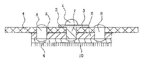
FIG. 1 is a sectional view of the heat radiating structure made by the process
of the
present invention;
FIG. 2 is an explosive view of the heat radiating structure made by the
process of the
present invention;
Appended Drawing Reference Signs
1 LED;
2 base
3 electrode welding leg
4 PCB board
5 copper plate
6 heat conducting plate
7 heat conducting column
8 fixation column
9 heat radiating plate
10 heat radiating fin
41 a first locating hole
42 a first fixation hole
61 a second locating hole
61 a second fixation hole
DETAILED DESCRIPTION OF THE PREFERRED EMBODIMENTS OF THE
INVENTION
Steps of the process of the present invention will be more fully understood
and
appreciated from the following detailed description, taken in conjunction with
the drawings, in
which FIG. 1 and FIG. 2 are integral view and explosive view of the heat
radiating structure
made by the process of the present invention respectively.
The process of making a heat radiating structure for high-power LED in the
present
invention comprises the following steps.
(1) Provide a PCB board 4, a heat conducting plate 6, a heat radiating plate
9, and other
components or materials; wherein the heat conducting plate 6 is made from red
copper based
4
'
CA 02818087 2013-05-15
Doc. No.: 152-5 CA/PCT
Patent
material, aluminum based material and the like, the heat conducting column 8
is made from red
copper based material and the heat radiating plate 9 is made from aluminum
based material or
copper based material. Both aluminum based material and copper based material
function well in
thermal conduction and radiation, the heat conducting plate 6 and the heat
radiating plate 9 in the
present invention are made from aluminum based material and the copper based
material, which
helps to achieve the objective of the present invention. Obviously, main
bodies of the above-
described structures could be made from other metal materials having good
performance in
conducting and radiating heat. The heat conducting column 8 could be formed in
one piece with
the heat conducting plate 6, alternatively, the heat conducting column 8 could
be in the form of
an attachment piece which is fixedly welded to the heat conducting plate 6.
(2) Provide a first locating hole 41 and a first fixation hole 42 penetrating
both sides of
the PCB board 4, and weld a copper plate 5 to one side of the PCB board 4,
then coat the surface
of the copper plate 5 with a solder paste for fixedly welding the heat
conducting plate 6; solder
an electrode welding leg 3 to the other side of the PCB board 4 for connecting
with an electrode
portion at the bottom of the base 2 of the LED 1.
(3) provide a second locating hole 61 and a second fixation hole 62
penetrating both
sides of the heat conducting plate 6.
It is of note that in order to enhance the stability of the structure made by
the process of
the present invention, there could be a plurality of the first fixation holes
42 distributed
homogeneously around the first locating hole 41, similarly, there could be a
plurality of the
second fixation holes 62 distributed homogeneously around the second locating
hole 61. There is
a one-to-one correspondence between the first fixation holes 42 and the second
fixation holes 62
in terms of their position and number when both of them are multiple.
(4) overlay one side of the heat conducting plate 6 with one side of the PCB
board 4
which side is provided with the copper plate 5, and arrange the first locating
hole 41 in
correspondence with the position of the second locating hole 61, similarly,
arrange the first
fixation hole 42 in correspondence with the position of the second fixation
hole 62; use a fixation
column 8 to pierce through both of the first fixation hole 42 and the second
fixation hole 62 for
connecting together the PCB board 4 and the heat conducting plate 6 to form an
integral piece of
them. Wherein, when both of the first fixation hole 42 and the second fixation
hole 62 are
through-holes, the fixation column 8 is a rivet, and a riveted connection is
formed between the
5
CA 02818087 2013-05-15
Doc. No.: 152-5 CA/PCT
Patent
heat conducting plate 6 and the PCB board 4, then the rivet is pressed by
using a pressing
equipment; when both of the first fixation hole 42 and the second fixation
hole 62 are screw
holes, the fixation column 8 is a screw, and a screwed connection is formed
between the heat
conducting plate 6 and the PCB board 4.
In addition, the heat conducting plate 6 and copper plate 5 are fixedly welded
together,
which further enhances the stability and compactness of the structure made the
process of the
present invention.
(5) use the heat conducting column 7 to pierce through both of the first
locating hole 41
and the second locating hole 61, and one end of the heat conducting column 7
being protruded
outside one side of the PCB board 4, the length of the protruding end of the
conducting column 7
being greater than the thickness of the electrode welding leg 3; the shape and
size of the heat
conducting column 7 match with that of the first locating hole 41 and the
second locating hole
61, specifically, the cross section of the heat conducting column 8 could be
in the shape of round,
oval, triangle or hexagon, when the cross section of the heat conducting
column 7 has a round
shape, the inner wall of the first locating hole 41 as well as the second
locating hole 61 is provide
with internal screw threads, while the side wall of the heat conducting column
7 is provide with
external screw threads, the heat conducting column 7 is then threadedly
connected with the first
locating hole 41 and the second locating hole 61. The screwed connections
between the heat
conducting column 7 and both of the first locating hole 41 and the second
locating hole 61 could
improve the compactness of the heat radiating structure of the present
invention, and indirectly
improve its function in conducting and radiating heat.
(6) place the integral piece of the heat conducting plate 6 and the PCB board
4 produced
by the step (5) on a pressing equipment, and utilize the pressing equipment to
press the upper-
end surface of the heat conducting column 7 so as to adjust the length of the
protruding end of
the conducting column 7, and to make the upper-end surface of the conducting
column 7 and the
upper surface of the electrode welding leg 3 be on the same plane. This is a
key step in the
process of the present invention, as mentioned above, one end of the
conducting column 7 is
protruded outside one side of the PCB board 4 and the length of the protruding
end of the
conducting column 7 is greater than the thickness of the electrode welding leg
3, then the
pressing equipment is utilized to press the heat conducting column 7, hence
the upper-end
surface of the heat conducting column 7 is pressed and the length is adjusted
until the length of
6
CA 02818087 2013-05-15
Doc. No.: 152-5 CA/PCT
Patent
the protruding end of the conducting column 7 is equal to the thickness of the
electrode welding
leg 3. After the process of pressing, the area of cross section of the heat
conducting column 7
becomes larger, and an interference fit thus could be formed between the heat
conducting
column 7 and the first locating hole 41 as well as the second locating hole
61, so that the contact
area between the heat conducting column 7 and an heat conduction portion at
the bottom of the
base 2 becomes larger, which facilitates heat conduction; at the same time,
the upper-end surface
of the heat conducting column 7 and the upper surface of the electrode welding
leg 3 are on the
same plane, in this way, the bottom of the base 2 could fully engage with both
the upper-end
surface of the heat conducting column 7 and the upper surface of the electrode
welding leg 3,
hence, the electrode portion at the bottom of the base 2 could be fully
contacted with and welded
with the electrode welding leg 3, the heat conduction portion at the bottom of
the base 2 could
also be fully contacted with and welded with the upper-end surface of the heat
conducting
column 7, the contact area between the heat conduction portion at the bottom
of the base 2 and
the upper-end surface of the heat conducting column 7 should be as large as
possible to ensure
that heat produced from the LED 1 could be timely transferred from the
conducting column 7
and the heat conducting plate 6 to the heat radiating plate 9, and finally
dissipated from the heat
radiating plate 9.
(7) paste the inner side of the heat radiating plate 9 on the other side of
the heat
conducting plate 6 fixedly, the heat radiating plate 9 then could dissipate
the heat within the heat
conducting plate 6 timely. The outer side of the heat radiating plate 9 is
provided with a plurality
of heat radiating fins10 to provide an increased radiating area for the heat
radiating plate 9,
which further enhances the heat dissipating effect of the heat radiating plate
9.
The heat radiating structure made by the process of the present invention
could quickly
remove the heat produced from the LED, its thermal conduction effect as well
as thermal
radiation effect is greatly enhanced over that of the prior art.
7
CA 02818087 2015-01-23
Doc. No.: 152-5 CA/PCT
Patent
Table I. Measured temperatures of existing heat radiating structure (old) and
the heat
radiating structure made by the method of the present invention (new)
Input Environmental heat sink (old); aluminum heat
current temperature heat conducting substrate
radiating
column (new) (old); plate
heat
conducting
plate (new)
heat radiating 700 24.3 C 57.3 C 44.7 C 45.2 C
structure (old) mA
heat radiating 700 28 C 48.1/51 C 47.3/50.3 C
45.6/50.3 C
structure (new) mA
It can be seen from the above table, high-power LEDs respectively equipped
with new
heat radiating structure and old heat radiating structure were used, when the
same current
passed through the LEDs, the temperature of the heat conducting column of new
heat
radiating structure was obviously lower than that of the heat sink of old heat
radiating
structure though the environmental temperature was higher for new heat
radiating structure,
however, the temperatures of the heat conducting plate and the heat radiating
plate of new
heat radiating structure were respectively higher than that of the aluminum
substrate and the
heat radiating plate of old heat radiating structure, these results fully
proved that thermal
radiation effect of new heat radiating structure made by the process of the
present invention is
better than that of old heat radiating structure.
While the preferred embodiments of the invention have been described above, it
will
be recognized and understood that various modifications may be made therein,
and the
appended claims are intended to cover all such modifications which may fall
within the scope
of the invention.
8