Note : Les descriptions sont présentées dans la langue officielle dans laquelle elles ont été soumises.
CA 02825921 2015-07-07
AN IMPROVED BATTERY AND ASSEMBLY METHOD
[0002]
BACKGROUND
[0003] Battery technology, such as for electric vehicles and renewable
energy applications, is an area of intense research and development. Work has
focused on a number of technologies, with the most mature and successful ones
being lithium-ion and lead-acid batteries. Despite this work, cost remains a
central concern. Lithium ion, with its energy density, is attractive, but car-
makers can pay $1,000/kW=hr or more for a lithium-ion power source. Costs
remain high due to complex control and cooling systems in addition to
electronics used to improve safety. This cost is at least six times the United
States Advanced Battery Consortium (USABC) year 2020 target of $150/kW=hr.
Contrast this with contemporary lead-acid batteries (lead-acid batteries),
which
can have a cost of around $150/kW=hr for renewable energy storage, but their
limited energy density, cycle life, and efficiency in many cases discourages
their
use.
SUMMARY
[0004] Examples described below can improve upon contemporary
batteries by providing a lead-acid battery formed of one or more very thin
planar
battery electrodes (e.g., less than 1.0 millimeter) having active mass (e.g.,
lead or
a compound thereof) disposed on a very thin silicon substrate (e.g., less than
0.5
millimeters thick). Examples provide an improved battery that is less
expensive
1
CA 02825921 2013-07-26
WO 2012/155082
PCT/US2012/037598
and that performs better than other approaches. Because reliability and
support
infrastructure is important to widespread adoption, examples can employ
technologies based on proven batteries chemistries, such as lead-acid. A
plurality of these electrodes can be stacked together and packaged to provide
a
lead-acid that performs better than contemporary lead-acid batteries, such as
by
avoiding unbalanced ion depletion that can lead to nonreactive lead material.
Examples of these batteries, and methods of making and using them, are
described herein.
[0005] This summary is intended to provide an overview of subject
matter of the present patent application. It is not intended to provide an
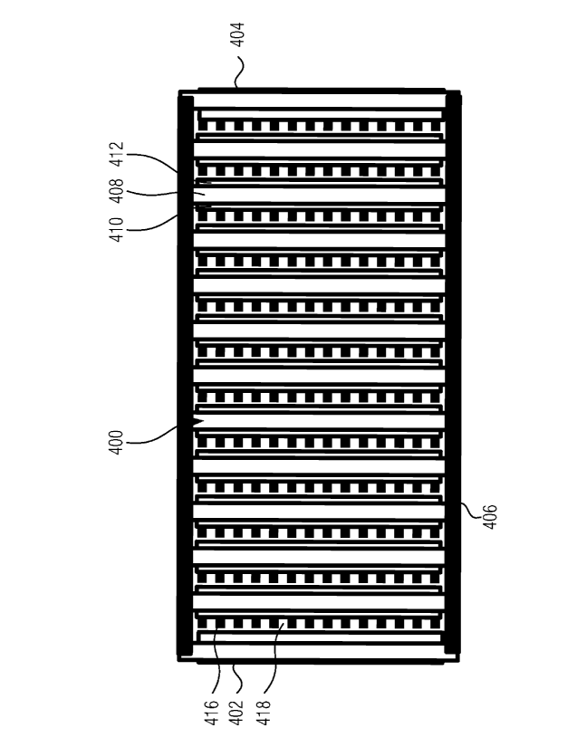
exclusive or exhaustive explanation of the invention. The detailed description
is
included to provide further information about the present patent application.
BRIEF DESCRIPTION OF THE DRAWINGS
[0006] The drawings, which are not necessarily drawn to scale, illustrate
generally, by way of example, but not by way of limitation, various
embodiments described in the present document.
[0007] FIG. lA shows a schematic representation of a battery layer
showing an aggregate of particles on a lead substrate, with arrows indicating
the
flow of ions, according to an example.
[0008] FIG. 1B shows a schematic representation of a simplified
representation of the layer of FIG. 1A, according to an example.
[0009] FIG. 2A shows a pore with low current density, according to
an
example.
[0010] FIG. 2B shows a pore with high current density, according to an
example.
[0011] FIG. 3 shows three layers with thinner active mass replacing
a
single layer, according to an example.
[0012] FIG. 4 shows a stacked or bipolar battery configuration,
including
alternating layers and spacers soaked with electrolyte, according to an
example.
[0013] FIG. 5 shows a method for assembling the stacked battery.
Battery layers and spacers are alternately stacked. The stack is placed in a
frame. The gap between the stack and frame is filled with adhesive. After the
2
CA 02825921 2013-07-26
WO 2012/155082
PCT/US2012/037598
adhesive sets, electrolyte is added (absorbed by the spacers) and a cap is
placed
on the top, according to an example.
[0014] FIG. 6 shows a method for assembling the stacked battery
using
removable spacers, according to an example.
[0015] FIG. 7A shows a top view of a plate-shaped spacer including
tapered edges, according to an example.
[0016] FIG. 7B shows a front view of a U-shaped spacer, according to
an
example.
[0017] FIG. 7C shows a fiberglass spacer having an edge lining of a
fiberglass spacers, according to an example.
[0018] FIG. 8 shows a flow chart of a battery assembly process,
according to an example.
[0019] FIG. 9 is a cross-sectional view of a battery layer with an
active
mass coating showing different layers, from left to right showing silicon,
nickel
silicide, barrier layer, lead oxide, according to an example.
[0020] FIG. 10 is a flow chart of the process for making the battery
layer,
including formation of a silicide contact and addition of layers to form a
barrier
to protect the layer from acid corrosion and to promote adhesion of the active
mass, according to an example.
[0021] FIG. 11A shows a mix of particles and a matrix, according to an
example.
[0022] FIG. 11B shows the matrix once the particles are removed,
according to an example.
3
CA 02825921 2013-07-26
WO 2012/155082
PCT/US2012/037598
[0023] FIG. 11C shows the matrix with plating, according to an
example.
[0024] FIG. 11D shows the matrix removed, according to an example.
[0025] FIG. 12 is a flow chart for formation of a porous active
mass,
according to an example.
[0026] FIG. 13 is a micrograph of a wax matrix with pores from
dissolved salt particles, according to an example.
[0027] FIG. 14 is a chart showing weight distribution in a
conventional
lead-acid battery.
DETAILED DESCRIPTION
[0028] Examples described herein can retain the low cost and market
acceptance of lead-acid batteries while improving their performance such as to
meet the needs of the electric vehicle and renewable energy markets. These
examples can take advantage of the acceptance and maturity of the lead-acid
battery and its infrastructure, providing a solution that is familiar to risk-
averse
markets. Many of the present examples may also be used to simplify
manufacture or design of other types of batteries.
[0029] To frame the contributions of the present subject matter, it
is
helpful to consider attributes of conventional lead-acid batteries.
Conventional
lead-acid batteries have a number of limitations. First, conventional lead-
acid
batteries should run at low current for high efficiency in charging and
discharging. This is because a reaction product, lead sulfate, can build up
and
block electrolyte diffusion, making active mass material (a.k.a. active
material)
located deep in the battery structure (referenced in the discussion of FIGS.
2A-B
below) inaccessible to chemical reaction. This effect is known as Peukert's
Law, which represents how battery capacity decreases as charging or
discharging
current increases. Due in part to this phenomenon, conventional lead-acid
batteries should be charged or discharged over a long time, e.g. tens of
hours, to
show improved efficiency. Unfortunately, most renewable energy storage and
vehicle applications desire much shorter discharge times, e.g., from 2 to 6
hours.
[0030] Second, conventional lead-acid batteries can demonstrate a
reduced life when cycled at deep discharge. Active mass can expand 20-60% in
volume as it converts from lead or lead oxide to lead sulfate. This expansion
creates stress and can cause delamination of a pasted active mass (that is,
active
4
CA 02825921 2013-07-26
WO 2012/155082
PCT/US2012/037598
mass applied as a paste, which is a conventional commercial process). Because
of this, conventional lead-acid batteries should be run in shallow discharge
of
from 40 to 60%. This can increase the number of batteries needed for some
applications, doubling it in some instances.
[0031] Third, high lead content can result in low energy density. Lead,
which is resistant to the sulfuric acid electrolyte, is used in conventional
batteries
as active mass, as well as being used in terminals or top leads and to provide
thick internal conductors to interconnect layers. Typical specific energies
for
lead batteries can be from 40 to 45 W=hr/kg, vs. a USABC target of 100
W=hr/kg. FIG. 14 shows the weight distribution in a conventional lead-acid
batteries used for traction. The subject matter described here can eliminate
or
greatly reduce the negative active mass, positive and negative grid, and top
lead
components, removing about half the lead found in a conventional lead-acid
battery. The subject matter described has the potential to eliminate weight
(around half in some examples) and can increase (doubling in some examples)
the energy density.
[0032] Fourth, conventional lead-acid batteries can be low voltage,
high
current devices. These properties are a poor match to higher voltage systems
used in vehicles and renewable energy systems.
[0033] Attempts to overcome limitations of conventional lead-acid
batteries have been met with obstacles. Low efficiency at high current affects
batteries made with the conventional approach of using active material applied
as a paste. This mature and low cost approach continues to be used in
contemporary lead-acid batteries designs, including high-end batteries.
[0034] Efforts have been made to improve cycle life. One approach is to
replace the negative active mass ("NAM") with a carbon electrode. Hydrogen
can intercalate in the carbon in a manner similar to lithium intercalation in
a
lithium-ion battery. This can reduce or eliminate shedding on that layer.
Another approach can integrate a super-capacitor with a conventional battery
to
provide extended life for repeated power bursts needed for start-stop cycles.
[0035] Lead content has been improved (i.e., decreased) and voltage
has
been improved (e.g., increased) with a bipolar lead-acid battery (such as
Blead-
acid batteries, or bipolar batteries). Examples can include a series-connected
stack of cells, operating at high voltage and low current. This configuration
can
5
CA 02825921 2013-07-26
WO 2012/155082
PCT/US2012/037598
reduce or eliminate heavy internal conductors used in low voltage, high
current
batteries, and can provide a high voltage output.
[0036] Blead-acid batteries promises advantages such as high energy
density by virtue of reduced conductor mass. However, several issues have
limited commercialization. These include cell-to-cell leakage, layer
degradation
in a corrosive environment that includes both the sulfuric acid electrolyte
and
oxygen radicals formed during charging, active mass shedding, and electrode
sagging that presents issues for layer separation.
[0037] An approach to address the layer degradation issue can use
ceramic conducting TiO2 substrates. The active material is a paste as in
conventional lead-acid batteries. Ceramic layers can be less susceptible to
sagging, but may be hard to manufacture in high volume at low cost.
[0038] However, even these approaches have shortcomings. Typical
Blead-acid batteries designs do not address Puekert's Law limitations. The
source of these limitations can be understood with the help of FIGS. 1A, 1B,
2A
and 2B.
[0039] FIG. lA shows a schematic representation of a battery layer
showing an aggregate of particles on a lead substrate, with arrows 110
indicating
the flow of ions, according to an example. The pasted active mass layer 102
can
include an aggregate of particles 104 disposed on a substrate 108, which can
be a
few microns in diameter. Electrolyte can flow through channels between the
particles. The channel diameter can be a few microns and the length can be
substantially similar to the thickness of the active mass, 1-3 millimeters in
some
examples.
[0040] FIG. 1B shows a schematic representation of a simplified
representation of the layer of FIG. 1A, according to an example. As depicted
in
FIG. 1B, channels 106 can be theoretically modeled as straight channels. At
low
currents, the electrolyte ions can diffuse the length of the channel with low,
or
even without, depletion, and the reaction can proceed along the full length of
the
channel 106. At high currents, the electrolyte ions can be consumed before
they
can diffuse the full length of the channel 106. As a consequence, at high
currents the active mass deep in the layer does not react as desired, and the
available energy, which is associated with available reactions with the AM,
can
decrease.
6
CA 02825921 2013-07-26
WO 2012/155082
PCT/US2012/037598
[0041] FIG. 2A shows a pore with low current density, according to
an
example. FIG. 2B shows a pore with high current density, according to an
example. In these examples, channel 206, which represent pores 208, have a
lead sulfate coating 210. The current at onset of ion depletion scales as
1/L2,
where L is the channel length. The narrowing 212 represents that more
reactions
have taken place than at less narrow portions.
[0042] FIG. 3 shows three layers with thinner active mass replacing
a
single layer, according to an example. One solution to the problem of
unbalanced ion depletion is to split the active mass into several thinner
layers, as
shown in FIG. 3, in which the length "L" shown in FIG. 2 has been reduced by a
factor of 1/X to provide a shorter channel 302. To compensate for the
reduction
in total channel length by the 1/X reduction, more channels 302', 302" can be
used. They may total X in number, but other numbers are possible. Such a
configuration can retain the same amount of active mass, so the battery can
retain the same or a similar capacity. Because of the shorter channels, the
battery can run at higher current while accessing a greater portion of the
active
mass. For example, dividing a single 1 millimeters thick active mass layer
into
three 0.3 millimeters thick active mass layers provides 9 times more current
without loss of capacity.
[0043] This approach and others disclosed herein can be used to
overcome shortcomings described above. New systems and methods described
herein provide battery layers with thin active mass layers. These layers can
be
closely spaced, and the amount of active mass can remain constant to retain a
desired battery capacity. Additionally, these thin active mass layers have
other
desirable attributes.
[0044] For example, a lead layer expands about 60% when converted to
lead sulfate, and the lead oxide layer expands about 20%. This expansion can
cause shedding of the active mass in deep cycling. A thinner layer has less
mechanical stress at the interface, and is less likely to shed, allowing the
battery
to operate reliably in deep cycling.
[0045] Examples disclosed herein provide a bipolar lead-acid battery
with layers that can be much thinner than conventional plates, which can
enable
balanced ion depletion. Silicon wafers can be used as substrates and provide
layers that are light, resistant to reaction with sulfuric acid, and that are
7
CA 02825921 2015-07-07
inexpensive. Active mass layers can be formed using plating or electrophoretic
deposition instead of pasting, enabling controlled formation of thin layers.
The
composition can be varied in depth to provide for selected critical properties
such as porosity, grain size, and stress. Contact and barrier layers can be
included. A sacrificial template process is described by way of example to
provide controlled porosity, employing one or both of deposition of a
sacrificial
layer and co-deposition using electrophoresis. Methods to package the battery
are also described, and can include sealing a stack of layers in a molded
form,
adding electrolyte, and affixing a cover.
[0046] Examples provide a bipolar lead-acid battery design that enables
the use of thin layers to provide a battery with an increased layer density
over
that of conventional batteries. Examples allow spreading the active mass over
a
large number of thin layers to reduce the effect of Puekert's Law, enabling
deep
cycling (i.e., balanced ion depletion) with reduced shedding of active mass.
Examples provide a high voltage output suitable for electric vehicle and
renewable energy systems. Examples use less (half in some examples) of the
lead of conventional lead-acid batteries, which can increase (double in some
examples) energy and power density.
[0047] FIG. 4 shows a stacked or bipolar battery configuration,
including
alternating plates and separators or spacers soaked with electrolyte,
according to
an example. A electrochemical battery has two terminals: a cathode (positive)
and anode (negative). A reduction reaction occurs at the cathode and an
oxidation reaction occurs at the anode. The battery potential is the sum of
the
half-reaction voltages. In the case of lead-acid, the positive plate is
typically
lead oxide, and the half-reaction voltage is about 1.6 volts. The negative
plate is
typically lead, and the half-reaction voltage is 0.4 volts.
[0048] A battery cell includes, at a minimum of an anode and cathode.
Voltages for cells wired in series are additive. Accordingly, 10 lead-acid
cells
connected in series can provide 20 volts (e.g., 10 cells x 2 volts/cell). In
an
example series connection, the string can include a series of anodes connected
to
cathodes, with the intervening electrolytes electrically isolated.
[0049] The example includes a stack 400 of layers such as plates 408
packaged with spacers 406. The stack 400 can include one or more anodes 410
separated from cathodes 412, such as by spacers or separator. Gaps between the
8
CA 02825921 2015-07-07
plates can be filled with sulfuric acid electrolyte. The electrolyte masses or
volumes can be electrically isolated so that the plates can be in series. The
spacer material can be fiberglass, which is porous and can absorb sufficient
sulfuric acid. The plate spacing can be 0.5 millimeters.
[0050] Separators or spacers 406 can prevent shorting of the plates, and
can be thin sheets of fiberglass. In some cases, the plates are stiff, and in
some
of those examples spacers are not necessarily used. Electrolyte, which can be
sulfuric acid, can be disposed in a space between plates. Electrolyte can be
soaked into the spacers.
[0051] If multiple electrolyte masses or volumes can be electrically
isolated from one another, and there is a conduction path from the anode to
the
cathode, such as through the use of plates that are conductive, the stack can
form
a series-connected arrangement of cells. Voltage can be equal to (N-1)Vca,
where N is the number of plates (with one at each end for connection to the
positive 404 and negative 402 terminals), and Well is the voltage of a single
cell.
For example, the cell voltage for the lead-acid reaction can be around 2
volts.
Accordingly, a battery having 101 plates can have a voltage of 200 volts. A
housing 406 is shown, mechanically maintaining multiple cells in a stack.
[0052] Examples can include electrically conducting substrates with
an
anode on one side and cathode on the other. The substrate can act as the
conductor or "wire" to connect the cells together while isolating the
electrolytes
from one-another. In some examples it is possible to eliminate the lead
electrode
entirely by using a carbon or silicon counter-electrode. This can provide even
higher energy density. Such examples can use bare silicon or carbon coated
silicon as the counter electrode to the lead oxide electrode.
[0053] Note that the cathode can provide most of the cell voltage.
Some
cases omit lead as the material for the half cell reaction at the anode while
providing a place for a reduction reaction to occur on that side of the cell.
One
way to accomplish this is to allow protons from the electrolyte solution to
react
(intercalate), as occurs in other types of batteries such as lithium ion. This
reaction operates in both carbon and silicon. In such a case, the cell voltage
can
be at least 1.6 volts (the cathode half-cell potential), but the mass and
weight of
the lead on the anode can be reduced or eliminated, resulting in an increase
in
power and energy density and reductions in cost and toxic material content.
Life
9
CA 02825921 2013-07-26
WO 2012/155082
PCT/US2012/037598
can also be extended because lead suffers the greatest expansion when it
converts to lead sulfate, and therefore undergoes the greatest stress. The
loss of
voltage can easily be made up by adding more series-connected cells.
[0054] An exposed leftmost electrode 402 can serve as a terminal,
such
as for coupling electrically and mechanically with electronics. The exposed
major face of the rightmost terminal 404 can serve as an electrode of the
opposite polarity, and can serves as a terminal as well. However, in some
examples, the stack is disposed in a housing or container and is connected to
electronics outside the housing via one or more feedthroughs extending through
the housing.
[0055] The anode is shown having a plurality of protrusions 416
defining channels 418. However, the present subject matter is not so limited,
and examples in which the cathode has protrusions are also contemplated, as
are
examples in which no protrusions are used.
[0056] An unexpected result is that such a battery can in some examples,
use silicon wafers with standard solar cell texture. Some examples use
textured
silicon, such as cut wafers. As-cut silicon wafers, originally used for solar
cells,
can be used as the substrates for the electrodes. These wafers are light
(about a
quarter the density of lead), can be resistant to sulfuric acid corrosion, and
can be
generally available at low cost by virtue of their high volume of use. As-cut
wafers can have a surface roughness that provides good adhesion, such as for
mechanically joining with a coating. For example, multi-crystal (MC) wafers
can be formed by iso-texturing, such as in a bath of hydrofluoric acid and
nitric
acid.
[0057] Multi-crystalline wafers can provide a square form factor and
lower cost. Single crystal wafers can also be used. Single crystals can have a
pyramidal texture, typically formed with a potassium hydroxide ("KOH")
/isopropyl alcohol etch. Because large grain size is not as important, MC
wafers
can be made more rapidly than they are for solar applications, which can
provide
for lower cost. A lower cost metallurgical grade silicon can be used, as its
purity
is compatible with battery applications disclosed herein. Other silicon, such
as
electronic, solar or semiconductor grade can be used, but are generally more
expensive.
CA 02825921 2013-07-26
WO 2012/155082
PCT/US2012/037598
[0058] In some examples, wafers can be doped. Doped wafers can have
a resistivity typically less than 1 11-cm. In some examples, the resistivity
can be
less than 0.001 11-cm. Lower resistivity can improve efficiency as battery
current flows through the wafers. Low resistivity can also improve the quality
of
contacts to the silicon. Dopants can be used, such as phosphorus, boron,
antimony or arsenic. Such wafers can be less than 500 um (0.5 millimeters)
thick, and can be less than 200um thick.
[0059] Wafers can be square, with an edge length of 156 millimeters
for
standard solar cell wafers, although rectangular wafers, or wafers with other
form factors such as clipped corners can also be used. Use of a standard edge
length can enable the use of wafers manufactured in high volume, which can
reduce cost, although other edge lengths can be used. Use of standard size
wafers can allow for the use of standard manufacturing equipment to handle and
process the wafers during battery manufacturing.
[0060] In certain examples, active mass can be formed on one or both
sides of a substrate. Lead can be plated onto both sides. One plated side can
be
masked and the other can be exposed to a sulfuric acid bath. While exposed, a
current can be run through such a bath using a lead negative electrode. Such
an
approach can convert the exposed side to lead oxide using a process termed
"forming."
[0061] In certain examples, only one side of the silicon substrate
is
coated with lead and converted to lead oxide or, alternately, coated with lead
oxide. In one-sided examples, the battery can have a lower voltage that an
example with active material lead coated on both sides. In some examples, the
half-cell potential for lead oxide to lead sulfate reaction can be 1.68 volts.
A
battery with lead coated on only one side can use less (e.g., half) lead, so
it can
be less toxic and lighter in weight. In addition, lead can expand more than
lead
oxide when converted to lead sulfate, so plates without a lead coated side can
experience less stress during cycling.
[0062] According to various examples, either one or both sides can be
coated with active mass. Other materials can be used as active mass and the
use
of the silicon plates is not exclusive to lead-acid type batteries. In some
instances configured as single-sided, hydrogen can intercalate into the
silicon on
the opposite electrode, much as lithium does in a lithium-ion battery. Note
that a
11
CA 02825921 2013-07-26
WO 2012/155082
PCT/US2012/037598
silicon surface can be coated with an inert material such as carbon, and
hydrogen
can intercalate into the carbon. Such intercalation can be beneficial, as it
can
help a cell resist bulging due to gas production.
[0063] FIG. 5 shows a method for assembling the stacked battery. On
the left, a side view of battery plates and spacers alternately stacked is
shown.
As illustrated, alternating layers of plates 502 and fiberglass spacers 504
can be
stacked, as shown in the left drawing in FIG. 5. Note that there can be a
plate at
each end to form the positive and negative terminals or poles of the battery.
The
battery stack can be placed in a U-shaped frame 506 that provides three sides.
An adhesive that is resistant or impervious to sulfuric acid, such as epoxy or
any
of a number of plastics resistant to sulfuric acid, such as polypropylene, can
be
injected into the space 508 between the u-shaped frame 506 and the battery
stack
500. After the adhesive has set electrolyte can be added and a cover 510 can
be
put in place. In some examples, fiberglass spacers can resist or prevent
adhesive
from seeping into the space between the plates any more than a small region
near
the edges of the faces of the plates. It can be helpful to seal the edges 512
of the
stack so that the electrolyte masses (i.e., volumes with electrodes of
opposite
polarity on opposing sides) can be electrically isolated. In some cases, laser
cut
grooves can be formed near the periphery of the plates, using laser grooving
equipment common in solar cell manufacturing. Such grooves can be 10-20 lam
deep and on the order of 50 lam wide. This can provide a re-entrant structure
to
improve the quality of the edge seal.
[0064] FIG. 6 shows a method for assembling the stacked battery
using
removable spacers, according to an example. In some cases it is desirable to
have additional space in the gap 604 between the plates, thereby providing
room
for extra electrolyte. One example providing this space is the use of
removable
spacers 602, as shown in FIG. 6. A battery stack can be made with spacers 602
that extend out of the stack on the top side, as shown in the side view on the
left.
The battery stack can be placed in a U-shaped frame 606, shown in front view
in
the center, that provides three sides. An adhesive that is resistant or
impervious
to sulfuric acid, such as epoxy or any of a number of plastics resistant to
sulfuric
acid, can be injected into the space 608 between the U-shaped frame 606 and
the
battery stack 600. After the adhesive or plastic sets, the spacers can be
pulled
out, electrolyte can be added, and a cover 610 can be put in place. The cover
12
CA 02825921 2013-07-26
WO 2012/155082
PCT/US2012/037598
610 can have a vent to prevent gas pressure build-up if the battery is
overcharged, and can be removable to allow recharging of electrolyte.
[0065] FIG. 7A shows a top view of a plate-shaped spacer including
tapered edges, according to an example. The edges of the spacers can be
tapered, as shown in FIG. 7A, which is a top view. The tapered edges 706
extending away from a main body 708 can reduce contact area between the
spacer an another structure such as a frame, providing for easier removal.
They
also provide a tapered region that can be filled with the epoxy or plastic to
provide an improved seal.
[0066] FIG. 7B shows a front view of a U-shaped spacer, according to an
example. As illustrated in FIG. 7B, spacers can be U-shaped, with a spacer
portion 710 defining an inner void 712. Such a spacer can allow for removal by
pinching the ends 714 in the direction of the arrows and lifting the spacer
out of
a frame, a process that can permit air to enter the frame to ease spacer
removal.
[0067] FIG. 7C shows a fiberglass spacer having an edge lining of a
fiberglass spacers, according to an example. In some cases, fiberglass
separators
can wick the glue so that it extends excessively into the space between the
plates.
Forming an edge liner 704 around the fiberglass spacers 702, as shown in FIG.
7C, can prevent this. In some examples, the fiberglass can be melted to form a
glass frame that does not wick adhesive. In some examples, adhesive or plastic
can be applied to the rim of the spacers to form a frame consisting of set
adhesive. In some examples, the edge liner can be soft and flexible if an
appropriate adhesive such as silicone is used.
[0068] The spacers can be made of a non-stick material such as
Teflon,
or can have a Teflon coating to ease removal. They can also have holes through
the top that can be aligned so that one or more rods can be passed through the
set
of spacers, simplifying alignment and removal. A mold release material can be
applied to one or more surfaces to provide for easier removal.
[0069] In some examples, the edges of the silicon plates may have
nicks
or defects resulting during their manufacture. These nicks can cause the
plates
to break when handled. The plates can be coated with epoxy or plastic before
assembly. This is called pre-coating. It can protect the edges, to reduce the
risk
of breaking wafers. The coating can be by dipping or direct application. In
some examples, the coating thickness equals half the plate separation. In some
13
CA 02825921 2013-07-26
WO 2012/155082
PCT/US2012/037598
examples, the plates can be stacked and an additional layer of epoxy or
plastic
applied to form the outer housing of the battery. The pre-coating material can
be
a plastic substantially resistant to sulfuric acid. The sum of the thicknesses
of
the pre-coating on plate faces can be approximately equal a plate separation
between plates.
[0070] FIG. 8 shows a flow chart of a battery assembly process,
according to an example. The process can be used to produce the examples
discussed in FIGS. 4-6 and other disclosed herein. At 802, electrodes are
placed
into a stack. At 804, the electrode stack is placed in a frame. At 806,
adhesive is
added to adhere the stack to the frame. At 810, an optional step allows for
removal of at least some spacers. At 812, one or more interior space defined
between electrodes adhered to the frame can be filled with electrolyte. At
814, a
cover or top can be added to the frame to seal in the electrolyte.
[0071] FIG. 9 is a cross-sectional view of a battery plate with an
active
mass coating showing different layers, from left to right showing silicon,
nickel
silicide, barrier layer, lead oxide, according to an example. FIG. 9 shows an
example multiple layer stack. The figure shows a plate 900 comprising silicon
902, nickel silicide 904, a barrier layer 906 and lead oxide 908. It should be
noted that it is often desirable to remove any native oxide from the silicon
before
applying a layer. This can be done with sandblasting or using a chemical etch
such as buffered hydrofluoric acid.
[0072] It can be beneficial to form layers between the silicon
substrate
and the active mass. One benefit is to improve contact between the substrate
(e.g., silicon) and the active mass. Some examples interpose a silicide layer
between the substrate and the active mass. Some examples interpose a nickel
silicide layer between the substrate and the active mass. Such a layer can be
formed using an electroless nickel deposition or a vacuum process such as
evaporation or sputter deposition. Some examples include a heating cycle such
as at 500 C. Some examples heat for around 10 seconds. A silicide layer can be
formed on the opposite side to improve contact to the inert layer (e.g.,
carbon) or
to the electrolyte. In some examples, other silicides such as molybdenum,
titanium, tungsten and their alloys can be used instead of or in addition to
nickel.
[0073] Additional layers can be added for protecting the silicon
from
reaction with the electrolyte and to improve adhesion of the active mass to
the
14
CA 02825921 2013-07-26
WO 2012/155082
PCT/US2012/037598
substrate. Such layers can include TiN, TaN, molybdenum selenide, tin or
chrome, and can be formed on one or both sides of the substrate. Methods of
deposition include, but are not limited to, sputtering, reactive sputtering or
evaporation. Barrier or adhesion layers can be relatively thin, such as from
20 to
100 nm.
[0074] FIG. 10 is a flow chart of the process for making the battery
plate,
including formation of a silicide contact and addition of layers to form a
barrier
to protect the plate from acid corrosion and to promote adhesion of the active
mass, according to an example. The process can be used on one or both faces of
a layer. At 1002, the method starts by providing a silicon substrate. At 1004,
the substrate can be cleaned to remove contamination and organic deposits.
Cleaning solutions that can be used include a mixture of sulfuric acid and
hydrogen peroxide to remove organics. The surface can also be etched in
hydrofluoric acid to remove any oxide layer that forms after the
sulfuric/peroxide clean, or can be sandblasted. At 1006, electroless nickel
can be
deposited. Optionally, electroless nickel can be can be vacuum deposited as
described above. At 1008, the deposit can be baked. Such a deposit can be
heated at 300-700 C, such as for 30 seconds to form a silicide contact layer.
At
1010, a barrier can be deposited. The barrier can be plated or sputtered,
among
other methods of forming. At 1012, an adhesion and/or barrier layers can be
deposited. At 1014, the active mass can be formed using methods described
herein. At 1016, the active mass can be conditioned, for example, to turn it
from
lead to lead oxide. In some examples, lead can be plated directly to the
silicon.
The lead can optionally be heated at 200 C for 5 minutes to improve contact
and
adhesion.
[0075] Examples can form an active mass with controlled porosity and
pore size. In some examples, the active mass can be plated. The active mass
can
be less than 1 millimeter thick. Some examples are from 0.2 to 0.3 millimeters
thick.
[0076] In some examples, the active mass can include lead(IV) oxide,
Pb02. The notation lead "(IV)" refers to lead with a valence of +4. A plated
material can also include lead, which can be electrolytically converted to
Pb02
using forming or conditioning. In some conditioning processes, current can be
CA 02825921 2015-07-07
run through the plate in a 6 molar sulfuric acid bath to convert it to lead
sulfate.
The current can be reversed to form lead oxide on a positive plate.
[0077] FIGS. 11A-C show a pictorial representation of the process of
making a porous active mass, according to an example. A deposition can be
made porous using various methods. In some examples, additives can be put in
the plating solution, such as those used to make a matte finish plating. In
some
examples, a sacrificial layer 1102 can be used. A mix of fine soluble
particles
1104 and a matrix material 1106 such as a cured resin such as paraffin wax or
a
polymer such as etch-resist can be prepared. The particles 1104 can have the
same size as the active mass grains, which can be around 5 p.m diameter. They
can be of a soluble material such as a crystalline salt, sodium chloride being
one
example. The mix can be applied to the substrate 1108, which can be heated to
allow the matrix (e.g., paraffin) to flow. The mix can be allowed to solidify,
by,
for example, cooling or evaporation of organic constituents. The wafer can be
placed in water so that the soluble particles 1104 dissolve. Such a process
can
produce a porous organic matrix 1106.
[0078] Once the porous matrix is created, the wafer can be placed in a
plating bath. The active mass material can be plated into the pores. The
matrix
1106 can be thicker than the plating 1110 thickness, which can be determined
by
the plating time and current. The matrix can be dissolved in a solvent to
leave
the porous active mass layer, which can be conditioned to form lead(IV) oxide
if
the original plating material was lead.
10079] In some examples, electrophoretic deposition can be used to
deposit the active mass. Electrophoresis is a process in which charged
particles
can be attracted to an electrode. In an example process a suspension of active
mass particles can be made in an ethanol bath, such as by using ultrasonic
agitation. One benefit of ethanol, and compositions thereof, is that it is a
poor
conductor of electricity, so a field can be established across the bath. A
small
amount of sulfuric acid can be added to the suspension, for example 0.5
milliliters per 100 milliliters of bath. Such an addition can provide a source
of
ions to charge suspended active mass particles. The electrode to be coated can
be placed in the bath and connected to the negative terminal of a voltage
source,
such as a 50-200 volt source, with an electrode spacing on the order of 2-5
centimeters. The potential urges active mass particles to the surface, where
they
16
CA 02825921 2013-07-26
WO 2012/155082
PCT/US2012/037598
deposit. A coated plate can be baked at a temperature exceeding 100 C. Some
examples are baked at 200 C for 30 minutes. Baking can drive ethanol out of
the coating.
[0080] Other materials can be co-deposited with this method,
including,
but not limited to, fiber and chemical binders. Such materials can improve
adhesion and the integrity of the film. Integrity as used herein refers to
resistance to flaking or decomposition of the active mass layer. A soluble
species such as salt grains can also be co-deposited, and can be dissolved as
described above to control film porosity. This has the advantage of reducing
or
eliminating the need for sacrificial paraffin and subsequent plating steps.
[0081] FIG. 12 is a flow chart for making a porous active mass,
according to an example. The flowchart can be used to make the apparatus of
FIG. 11. At 1202, a filled matrix can be applied to a substrate. At 1204,
filler in
the matrix can be dissolved. At 1206, the matrix can be plated. At 1208 the
matrix can be dissolved. At 1210 the remaining material can be conditioned.
[0082] FIG. 13 shows a micrograph 1300 of a paraffin matrix 1302
with
holes 1304 left behind after salt crystals have been dissolved. The ratio of
matrix material to particles can determine the porosity. Particle size and
shape
can determine the pore size. The mixture can contains 50-70% solids. A high
solid fraction can encourage the formation of pores that are continuous, which
enables thorough plating throughout the matrix. In some cases matrix material
wets the top surface, in which can the surface can be lightly scraped to
expose
salt.
[0083] The consistency of the active mass can be varied in depth.
For
example, multiple sequential depositions can be layered on top of one another.
During a deposition, parameters can be altered, making it possible to vary
parameters such as grain size, porosity, composition, or film stress.
VARIOUS NOTES & EXAMPLES
[0084] Example 1 can include or use subject matter (such as an
apparatus, a method, a means for performing acts, or a device readable medium
including instructions that, when performed by the device, can cause the
device
to perform acts), such as a stack of electrodes, including: a first electrode
including a silicon substrate and an active material or active mass disposed
on
17
CA 02825921 2013-07-26
WO 2012/155082
PCT/US2012/037598
the silicon substrate, a second electrode disposed in the stack in alignment
with
the first electrode, and a separator disposed between the first electrode and
the
second electrode. The example can include a housing, with the stack of
electrodes disposed in the housing, electrolyte filling the housing and in
contact
with the first electrode and the second electrode, a seal coupled between the
housing and the stack to define an interior space extending between the first
electrode and the second electrode, the seal adapted to resist the flow of
electrolyte from the interior space, a cover coupled to the housing, and a
cover
seal adapted to resist the flow of the electrolyte from inside the interior
space.
[0085] Example 2 can optionally can optionally include the subject
matter of any of the preceding examples 1, wherein a major face of the first
electrode is exposed to an exterior, the second electrode is of a different
polarity,
and a second major face of the second electrode is exposed to an exterior,
opposite the first major face.
[0086] Example 3 can optionally include the subject matter of any of the
preceding examples, wherein the active material includes lead (or a lead
compound) and the electrolyte includes sulfuric acid.
[0087] Example 4 can optionally include the subject matter of any of
the
preceding examples in which at least one intervening layer is disposed between
the substrate and the active material.
[0088] Example 5 can optionally include the subject matter of any of
the
preceding examples wherein the intervening layer is formed of at least one of
a
group including TiN, TaN, molybdenum selenide, tin and chrome.
[0089] Example 6 can optionally include the subject matter of any of
the
preceding examples wherein the intervening layer includes a silicide.
[0090] Example 7 can optionally include the subject matter of any of
the
preceding examples wherein the silicide includes tungsten, titanium, nickel or
molybdenum.
[0091] Example 8 can optionally include the subject matter of any of
the
preceding examples, wherein the substrate is less than 0.5 millimeters thick
and
the active material is less than 0.5 millimeters thick.
[0092] Example 9 can optionally include the subject matter of any of
the
preceding examples, wherein the substrate has a cut surface onto which the
active material is disposed.
18
CA 02825921 2013-07-26
WO 2012/155082
PCT/US2012/037598
[0093] Example 10 can optionally include the subject matter of any
of
the preceding examples, wherein the active material is porous.
[0094] Example 11 can optionally include the subject matter of any
of
the preceding examples, wherein a major face of the substrate has a
rectangular
perimeter, with side lengths of approximately 156 millimeters.
[0095] Example 12 can optionally include the subject matter of any
of
the preceding examples, including forming a battery electrode by disposing an
active material coating onto a silicon substrate, assembling the battery
electrode
into a stack of battery electrodes, the battery electrode separated from other
battery electrodes by a separator, disposing the stack in a housing, filling
the
interior space with electrolyte, and sealing the housing to resist the flow of
electrolyte from the interior space.
[0096] Example 13 can optionally include the subject matter of any
of
the preceding examples in which the plated coating is lead, and further
including
oxidizing the coating after application to form lead(IV) oxide.
[0097] Example 14 can optionally include the subject matter of any
of
the preceding examples, including forming a silicide between the substrate and
the active material by disposing a nickel onto the substrate and heating the
substrate.
[0098] Example 15 can optionally include the subject matter of any of
the preceding examples wherein disposing the nickel includes plating the
nickel
including applying the nickel using electroless deposition.
[0099] Example 16 can optionally include the subject matter of any
of
the preceding examples in which the silicide is formed by sputtering or
evaporating a metal and heating the substrate.
[00100] Example 17 can optionally include the subject matter of any
of
the preceding examples, wherein the active material is a porous plated active
material formed by: disposing a sacrificial layer of matrix material and
particles
onto the substrate, dissolving the particles to form a matrix with pores,
plating
active material into at least some pores, and dissolving the matrix.
[00101] Example 18 can optionally include the subject matter of any
of
the preceding examples, wherein disposing the active material onto the
substrate
includes applying the substrate using electrophoresis.
19
CA 02825921 2013-07-26
WO 2012/155082
PCT/US2012/037598
[00102] Example 19 can optionally include the subject matter of any
of
the preceding examples, including mechanically fixing the stack to the housing
to define an interior space, with the separator disposed in the interior
space, and
removing the separator.
[00103] Example 20 can optionally include the subject matter of any of
the preceding examples, wherein disposing the active material includes
electrophoretic co-deposition of the active material along with a sacrificial
material, and defining a porous active material by dissolving the sacrificial
material after electrophoretic co-deposition.
[00104] Example 21 can optionally include the subject matter of any of
the preceding examples, in which the silicon substrate is highly doped.
[00105] Example 22 can optionally include the subject matter of any
of
the preceding examples in which the silicon resistivity is less than 1 11-cm.
[00106] Example 23 can optionally include the subject matter of any
of
the preceding examples which the substrate has an as-cut surface.
[00107] Example 24 can optionally include the subject matter of any
of
the preceding examples which the silicon has a standard solar cell texture.
[00108] Example 25 can optionally include the subject matter of any
of
the preceding examples which the silicon is metallurgical grade material.
[00109] Example 26 can optionally include the subject matter of any of
the preceding examples which the substrate is multi-crystal silicon.
[00110] Example 27 can optionally include the subject matter of any
of
the preceding examples including a process for applying an active mass coating
to a silicon battery plate in which the coating is plated or deposited using
electrophoresis.
[00111] Example 28 can optionally include the subject matter of any
of
the preceding examples in which the plated or electrophoresis deposited
coating
is less than 1 millimeters thick.
[00112] Example 29 can optionally include the subject matter of any
of
the preceding examples, including intervening layers between the silicon
substrate and active mass to promote adhesion of the active mass to the
battery
plate.
CA 02825921 2013-07-26
WO 2012/155082
PCT/US2012/037598
[00113] Example 30 can optionally include the subject matter of any
of
the preceding examples in which an additive is included in the plating
solution to
promote porosity.
[00114] Example 31 can optionally include the subject matter of any
of
the preceding examples in which a sacrificial layer is applied to the battery
plate,
said sacrificial layer consisting of a matrix material and particles, said
particles
being subsequently dissolved to form a matrix with pores, at least a portion
of
said pores being then filled by plating and said matrix being subsequently
dissolved, in which the matrix material is at least one of wax and a polymer.
[00115] Example 32 can optionally include the subject matter of any of
the preceding examples in which said particles are a crystalline salt.
[00116] Example 33 can optionally include the subject matter of any
of
the preceding examples in which the crystalline salt is sodium chloride.
[00117] Example 34 can optionally include the subject matter of any
of
the preceding examples that also includes porous spacers between plates.
[00118] Example 35 can optionally include the subject matter of any
of
the preceding examples in which the porous spacer material includes
fiberglass.
[00119] Example 36 can optionally include the subject matter of any
of
the preceding examples in which a stack is formed including alternating
battery
plates, porous spacers, and removable spacers, said stack is then placed in a
containment fixture, sealant is applied to the periphery of said stack, and
said
removable spacers are removed after said sealant sets.
[00120] Example 37 can optionally include the subject matter of any
of
the preceding examples in which three sides are sealed, the spacers removed,
electrolyte added, and a top cover placed on the battery.
[00121] Example 38 can optionally include the subject matter of any
of
the preceding examples in which one or more edges of the removable spacers are
tapered.
[00122] Example 39 can optionally include the subject matter of any
of
the preceding examples in which a release coating is applied to the removable
spacers.
[00123] Example 40 can optionally include the subject matter of any
of
the preceding examples in which the removable spacers have a U-shape so that
removal includes a step of pinching the ends of the U-shape toward each other.
21
CA 02825921 2013-07-26
WO 2012/155082
PCT/US2012/037598
[00124] Example 41 can optionally include the subject matter of any
of
the preceding examples in which the removable spacers are reusable.
[00125] Example 42 can optionally include the subject matter of any
of
the preceding examples in which a stack is formed including alternating
battery
plates and porous spacers, said stack is then placed in a containment fixture
and
sealant is applied to the periphery of said stack.
[00126] Example 43 can optionally include the subject matter of any
of
the preceding examples in which three sides are sealed, electrolyte added, and
a
top cover placed on the battery.
[00127] Example 44 can optionally include the subject matter of any of
the preceding examples in which the porous spacers have edge liners to prevent
absorption of the sealant into the spacers.
[00128] Example 45 can optionally include the subject matter of any
of
the preceding examples in which the edge liner is an adhesive.
[00129] Example 46 can optionally include the subject matter of any of
the preceding examples in which the adhesive is silicone.
[00130] Example 47 can optionally include the subject matter of any
of
the preceding examples in which the edge liner is formed by melting the edge
of
the fiberglass spacer.
[00131] Example 48 can optionally include the subject matter of any of
the preceding examples in which one face of the substrate is inert.
[00132] Example 49 can optionally include the subject matter of any
of
the preceding examples in which the inert face is silicon
[00133] Example 50 can optionally include the subject matter of any
of
the preceding examples in which the inert face is coated with carbon.
[00134] Example 51 can optionally include the subject matter of any
of
the preceding examples in which the inert face is a silicide.
[00135] Example 52 can optionally include the subject matter of any
of
the preceding examples in which the active mass on at least one side is
applied
using electrophoresis.
[00136] Example 53 can optionally include the subject matter of any
of
the preceding examples in which the active mass material includes lead oxide.
22
CA 02825921 2013-07-26
WO 2012/155082
PCT/US2012/037598
[00137] Example 54 can optionally include the subject matter of any
of
the preceding examples in which active mass is baked at a temperature
exceeding 100 C after electrophoretic deposition.
[00138] Example 55 can optionally include the subject matter of any
of
the preceding examples in which an intervening layer is disposed between the
electrophoretic active mass deposition and the plate substrate.
[00139] Example 56 can optionally include the subject matter of any
of
the preceding examples in which plate material includes silicon.
[00140] Example 57 can optionally include the subject matter of any
of
the preceding examples, in which an electrode is formed by electrophoretic co-
deposition of an active mass material and a sacrificial material, said
sacrificial
material being dissolved after electrophoretic co-deposition in order to
increase
the porosity of the active mass layer.
[00141] Example 58 can optionally include the subject matter of any
of
the preceding examples active mass layer in which the active mass is co-
deposited with a second material, a function of said second material being to
improve a physical property of the active mass layer.
[00142] Example 59 can optionally include the subject matter of any
of
the preceding examples in which the physical property is adhesion.
[00143] Example 60 can optionally include the subject matter of any of
the preceding examples in which the physical property is integrity of the
active
mass layer.
[00144] Example 61 can optionally include the subject matter of any
of
the preceding examples including sand blasting the plate surface.
[00145] Example 62 can optionally include the subject matter of any of
the preceding examples in which a battery uses a plurality of plates, with at
least
two plate shaving edges being pre-coated.
[00146] Example 63 can optionally include the subject matter of any
of
the preceding examples in which the pre-coating material is epoxy.
[00147] Example 64 can optionally include the subject matter of any of
the preceding examples in which the pre-coating material is a plastic
substantially resistant to sulfuric acid.
23
CA 02825921 2013-07-26
WO 2012/155082
PCT/US2012/037598
[00148] Example 65 can optionally include the subject matter of any
of
the preceding examples in which the sum of the thicknesses of the pre-coating
on
plate faces approximately equals the plate separation.
[00149] Example 66 can optionally include the subject matter of any
of
the preceding examples in which a stack of plates is sealed after stacking to
provide an outer housing for the battery.
[00150] Example 67 can optionally include the subject matter of any
of
the preceding examples in which the sealing material is plastic.
[00151] Example 68 can optionally include the subject matter of any
of
the preceding examples in which the sealing material is epoxy.
[00152] Example 69 can optionally include the subject matter of any
of
the preceding examples in which the active mass consistency is varied with
depth through the use of either multiple sequential depositions or varying
deposition parameters through the deposition process.
[00153] Example 70 can include, or can optionally be combined with any
portion or combination of any portions of any one or more of Examples 1-69 to
include subject matter that can include means for performing any one or more
of
the functions of Examples 1-69, or a machine-readable medium including
instructions that, when performed by a machine, cause the machine to perform
any one or more of the functions of Examples 1-69.
[00154] Each of these non-limiting examples can stand on its own, or
can
be combined in various permutations or combinations with one or more of the
some examples.
[00155] The above detailed description includes references to the
accompanying drawings, which form a part of the detailed description. The
drawings show, by way of illustration, specific embodiments in which the
invention can be practiced. These embodiments are also referred to herein as
"examples." Such examples can include elements in addition to those shown or
described. However, the present inventors also contemplate examples in which
only those elements shown or described are provided. Moreover, the present
inventors also contemplate examples using any combination or permutation of
those elements shown or described (or one or more aspects thereof), either
with
respect to a particular example (or one or more aspects thereof), or with
respect
to some examples (or one or more aspects thereof) shown or described herein.
24
CA 02825921 2015-07-07
[00156]
[00157] In this document, the terms "a" or "an" are used, as is common
in
patent documents, to include one or more than one, independent of any other
instances or usages of "at least one" or "one or more." In this document, the
term "or" is used to refer to a nonexclusive or, such that "A or B" includes
"A
but not B," "B but not A," and "A and B," unless otherwise indicated. In this
document, the terms "including" and "in which" are used as the plain-English
equivalents of the respective terms "comprising" and "wherein." Also, in the
following claims, the terms "including" and "comprising" are open-ended, that
is, a system, device, article, composition, formulation, or process that
includes
elements in addition to those listed after such a term in a claim are still
deemed
to fall within the scope of that claim. Moreover, in the following claims, the
terms "first," "second," and "third," etc. are used merely as labels, and are
not
intended to impose numerical requirements on their objects.
[00158] Method examples described herein can be machine or computer-
implemented at least in part. Some examples can include a computer-readable
medium or machine-readable medium encoded with instructions operable to
conFIG. an electronic device to perform methods as described in the above
examples. An implementation of such methods can include code, such as
microcode, assembly language code, a higher-level language code, or the like.
Such code can include computer readable instructions for performing various
methods. The code can form portions of computer program products. Further,
in certain examples, the code can be tangibly stored on one or more volatile,
non-transitory, or non-volatile tangible computer-readable media, such as
during
execution or at other times. Examples of these tangible computer-readable
media can include, but are not limited to, hard disks, removable magnetic
disks,
removable optical disks (e.g., compact disks and digital video disks),
magnetic
cassettes, memory cards or sticks, random access memories (RAMS), read only
memories (ROMs), and the like.
[00159] The above description is intended to be illustrative, and not
restrictive. For example, the above-described examples (or one or more aspects
thereof) can be used in combination with each other. Other embodiments can be
CA 02825921 2013-07-26
WO 2012/155082
PCT/US2012/037598
used, such as by one of ordinary skill in the art upon reviewing the above
description. The Abstract is provided to comply with 37 C.F.R. 1.72(b), to
allow the reader to quickly ascertain the nature of the technical disclosure.
It is
submitted with the understanding that it will not be used to interpret or
limit the
scope or meaning of the claims. Also, in the above Detailed Description,
various
features can be grouped together to streamline the disclosure. This should not
be
interpreted as intending that an unclaimed disclosed feature is essential to
any
claim. Rather, inventive subject matter may lie in less than all features of a
particular disclosed embodiment. Thus, the following claims are hereby
incorporated into the Detailed Description as examples or embodiments, with
each claim standing on its own as a separate embodiment, and it is
contemplated
that such embodiments can be combined with each other in various combinations
or permutations. The scope of the invention should be determined with
reference to the appended claims, along with the full scope of equivalents to
which such claims are entitled.
26