Note : Les descriptions sont présentées dans la langue officielle dans laquelle elles ont été soumises.
CA 02828364 2013-08-26
WO 2013/028232
PCT/US2012/026920
1
DESCRIPTION
PHOTODETECTOR AND UPCONVERSION DEVICE WITH GAIN (EC)
CROSS-REFERENCE TO RELATED APPLICATION
The present application claims the benefit of U.S. Provisional Application
Serial No.
61/447,406, filed February 28, 2011, which is hereby incorporated by reference
herein in its
entirety, including any figures, tables, or drawings.
BACKGROUND OF INVENTION
Existing night vision goggles are complex electro-optical devices that
intensify
existing light instead of relying on their own light source. In a typical
configuration, a
conventional lens, called the objective lens, captures ambient light and some
near-infrared
light. The gathered light is then sent to an image-intensifier tube. The image-
intensifier tube
can use a photo cathode to convert the photons of tight energy into electrons.
As the
electrons pass through the tube, more electrons can be released from atoms in
the tube,
multiplying the original number of electrons by a factor of thousands, often
accomplished
using a micro channel plate (MCP). The image-intensifier tube can be
positioned such that
cascaded electrons hit a screen coated with phosphors at the end of the tube
where the
electrons retain the position of the channel through which they passed. The
energy of the
electrons causes the phosphors to reach an excited state and release photons
to create a green
image on the screen that has come to characterize night vision. The green
phosphor image
can be viewed through an ocular lens where the image is magnified and focused.
Recently, light up-conversion devices have attracted a great deal of research
interest
because of their potential applications in night vision, range finding, and
security, as well as
semiconductor wafer inspections. Early near infrared (NIR) up-conversion
devices were
mostly based on the heterojunction structure of inorganic semiconductors where
a
photodetecting and a luminescent section are in series. The up-conversion
devices are mainly
distinguished by the method of photodetection. Up-conversion efficiencies of
devices are
typically very low. For example, one NIR-to-visible light up-conversion device
that
integrates a light-emitting diode (LED) with a semiconductor based
photodetector exhibits a
maximum external conversion efficiency of only 0.048 (4.8%) W/W.
A hybrid
CA 02828364 2013-08-26
WO 2013/028232
PCT/US2012/026920
2
organic/inorganic up-conversion device, where an InGaAs/InP photodetector is
coupled to an
organic light-emitting diode (OLED), exhibits an external conversion
efficiency of 0.7%
W/W. Currently inorganic and hybrid up-conversion devices are expensive to
fabricate and
the processes used for fabricating these devices are not compatible with large
area
applications. Efforts are being made to achieve low cost up-conversion devices
that have
higher conversion efficiencies, although none has been identified that allows
sufficient
efficiency for a practical up-conversion device. Hence there remains a need to
achieve higher
efficiencies of an up-conversion device that can employ IR photodetector and
light emitter
materials that are currently available and can be fabricated in a cost
effective manner.
BRIEF SUMMARY
Embodiments of the invention are directed to an IR photodetector with gain
comprising a cathode, an IR sensitizing material layer, a charge
multiplication layer (CML),
and an anode. The CML separates the IR sensitizing material layer from the
cathode and has
a LUMO level > 0.5 eV higher than the cathode's Fermi level, absent IR
radiation.
Alternately, the CML separates the IR sensitizing material layer from the
anode and has a
HOMO level > 0.5 eV lower than the anode's Fermi level, absent IR radiation.
In
embodiments of the invention, the IR sensitizing material layer comprises
PCTDA, SnPc,
SnPe:C60, AlPeCl, AlPcCI:C60, Ti0Pc, Ti0Pc:C60, PbSe QDs, PbS QDs, PbSe, PbS,
InAs,
InGaAs, Si, Ge, or GaAs and the CML comprises naphthalene tetracarboxylic
anhydride
(NTCDA), 2 , 9-Dimethy1-4,7 -dipheny1-1,10-phenanthroline (BCP), p-
bis(triphenylsily1)-
benzene (UGH2), 4,7-dipheny1-1,10-phenanthroline (BPhen), tris-(8-hydroxy
quinoline)
aluminum (A1q3), 3,5' -N,N' -dicarbazole-benzene (mCP), C60, tris [3 -(3 -
pyridyl)mesityl] -
borane (3TPYMB), ZnO or Ti02. In other embodiments of the invention, the IR
sensitizing
material layer comprises PbSe QDs or PbS QDs and the CML comprises oleic acid,
actylamine, ethanethiol, ethandithiol (EDT), or bensenedithiol (BTD). The IR
photodetector
with gain can further comprises a hole blocking layer that separates the IR
sensitizing
material layer from the anode.
Other embodiments of the invention are directed to up-conversion devices with
gain
that comprises the IR photodetector with gain and an organic light emitting
diode (OLED).
The OLED comprises the cathode, an electron transport layer (ETL), a light
emitting layer
(LEL), a hole transport layer (HTL), and the anode. The ETL comprises tris[3-
(3-pyridy1)-
CA 02828364 2013-08-26
WO 2013/028232
PCT/US2012/026920
3
mesityliborane (3TPYMB), 2,9-Dimethy1-4,7-dipheny1-1,10-phenanthroline (BCP),
4,7-
dipheny1-1,10-phenanthroline (BPhen), or tris-(8-hydroxy quinoline) aluminum
(A1q3). The
light emitting layer (LEI,) comprises tris-(2-phenylpyidine) iridium,
Ir(ppy)3, poly-[2-
methoxy, 5-(2'-ethyl-hexyloxy) phenylene vinylene] (IVIEH-PPV),
tris-(8-hydroxy
quinoline) aluminum (A1q3), or iridium (III) bis-[(4,6-di-fluoropheny1)-
pyridinate-
N,C21picolinate (FIrpic). The HTL comprises 1 ,1-bis[(di-4-
tolylamino)phenyl]eyelohexane
(TAPC), N,N'-diphenyl-N,N'(2-naphthyl)-(1,1'-pheny1)-4,4'-diamine (NPB), or
N,I\l'-
diphenyl-N.N'-di(m-toly1) benzidine (TPD). The up-conversion device with gain
can further
comprise an interconnect layer separating the IR photodetector with gain from
the OLED.
BRIEF DESCRIPTION OF DRAWINGS
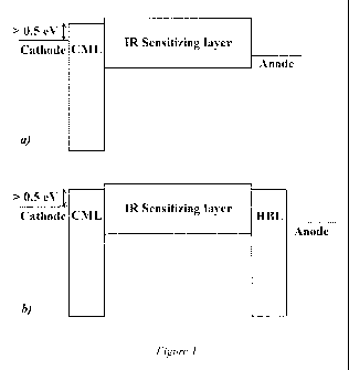
Figure 1 shows schematic energy band diagrams of IR photodetectors with gain,
according to embodiments of the invention, a) without and b) with a hole
blocking layer
Figure 2 shows schematic energy band diagrams of an IR photodetector with gain
a)
under applied voltage in the dark, b) under applied voltage upon initial IR
irradiation, and c)
under applied voltage and IR irradiation, where the hole accumulation in the
charge
multiplication layer (CML) reduces the energy level difference, which reduces
or removes
20 the energy difference between its LUMO and the Fermi level of the
cathode, which
promoting electron injection from the cathode, according to an embodiment of
the invention.
Figure 3 shows a) an IR photodetector with an organic IR sensitizing layer,
according
to an embodhnent of the invention, with a plot of the gain for the
photodetector as a function
of voltage and b) an IR photodetector with an inorganic IR sensitizing layer,
according to an
25 embodiment of the invention, with a plot of the gain for the
photodetector as a function of
wavelength at various applied voltages.
Figure 4 shows a schematic energy band diagram of an infrared-to-visible light
up-
conversion device with gain, according to an embodiment of the invention.
Figure 5 shows schematic energy band diagrams of an infrared-to-visible light
up-
30 conversion device with gain, according to an embodiment of the
invention, a) under applied
voltage in the dark, b) under applied voltage upon initial IR irradiation, and
c) under applied
voltage and IR irradiation, where the hole accumulation in the CML reduces the
energy level
CA 02828364 2013-08-26
WO 2013/028232
PCT/US2012/026920
4
difference, which reduces or removes the energy difference between its LUMO
and the Fermi
level of the cathode such that electrons injected by the cathode and generated
by the
photodetector are provided to the visible light emitting layer (LEL).
DETAILED DISCLOSURE
Embodiments of the present invention are directed to an up-conversion device
comprising a photodetector with gain. By the imposition of gain, the signal
from the IR
photodetector can be amplified such that the light emitter of the up-
conversion device emits a
higher intensity with greater contrast. Embodiments of the invention are
directed towards the
1 0 achievement of gain by coupling the photodetector with a charge
multiplication layer (CML).
A schematic for a photodetector with gain is shown in Figure la, where the IR
sensitizing
layer, the photodetector, is separated from the cathode by a CML that is
characterized by a
deep highest occupied molecular orbital (HOMO) and a lowest unoccupied
molecular orbital
(LUMO) with an energy level, relative to the work function of the cathode,
that results in an
injection barrier in the absence of IR radiation of at least 0.5 eV.
Optionally, in an
embodiment of the invention, a hole blocking layer (HBL) is situated between
the IR
sensitizing layer and the anode, as shown in Figure lb.
The manner in which the photodetector with gain, according to an embodiment of
the
invention, functions is schematically illustrated in Figure 2a. With an
applied bias in the
dark, where no IR radiation illuminates the IR sensitizing layer, there is
little or no injection
of electrons from the cathode because of the CML's >0.5 eV barrier, as
indicated in Figure
2a. As illustrated in Figure 2, the device acts as an electron only device.
Although this
device, and most devices of this disclosure, are directed to an electron only
device, it should
be understood by those skilled in the art that a device that acts as a hole
only device in the
absence of IR radiation can be constructed in like manner for a device that
has gain by
imposition of the opposite electrical bias and a CML where an energy level
relative to the
work function of the anode promoting accumulation of electrons rather than
holes. Upon IR
irradiation, the IR sensitizing layer generates electron-hole pairs with the
electrons flowing to
the anode because of the applied bias, as illustrated in Figure 2b. The
counter flow of
photogenerated holes results in the accumulation of holes at the CML, which
diminishes the
barrier for electron injection into the CML to less than 0.5 eV as shown in
Figure 2c and
significantly increases the electron current towards the anode under the
applied bias.
CA 02828364 2013-08-26
WO 2013/028232
PCT/US2012/026920
In embodiments of the invention, the IR photodecting layer can be inorganic.
In an
exemplary up-conversion device, a layer of PbSe quantum dots (QDs) can be
employed as
the IR photodetector and MEH-PPV can be employed as the eleetrolumineseent
OLED. In
addition to PbSe, other QDs that can be employed include, but are not limited
to, PbS. Other
5 inorganic materials that can be employed as IR photodetectors include,
but are not limited to,
continuous thin films of: PbSe, PbS, InAs, InGaAs, Si, Ge, or GaAs. In
embodiments of the
invention, the IR photodetector is an organic or organometallie comprising
material
including, but not limited to, perylene-3,4,9, i O-tetracarboxylic-3,4,9, 1 -
di anhydride
(PTCDA), tin (II) phthalocyanine (SnPc), SnPe:C60, aluminum phthalocyanine
chloride
(A1PeC1), A1PeC1:C60, titanyl phthalocyanine (Ti0Pc), and TiON:C60.
By including the CML, the IR photodetector displays gain such that the
efficiency of
an up-conversion device is improved. An exemplary CML is naphthalene
tetracarboxylic
anhydride (NTCDA). Other CMLs that can be employed in embodiments of the
invention
include, but are not limited to, 2,9-Dimethy1-4,7-dipheny1-1,10-phenanthroline
(BCP), p-
bis(triphenylsilyl)benzene (UGE12), 4,7-dipheny1-1,10-phenanthroline (BPhen),
tris-(8-
hydroxy quinoline) aluminum (A1q3), 3 ,5 ' -N,N'-dicarbazole-benzene (mCP),
C60, tris [3 -(3 -
pyridy1)-mesityl]borane (3TPYMB), ZnO, or Ti02. When the IR photodetector is
inorganic,
the CML can be an organic ligand, such as oleic acid that caps the inorganic
photosensitive
material.
The inclusion of the CML significantly improves the efficiency of the
photodetector. For example, as shown in Figure 3a, using a PTCDA IR
sensitizing layer and
a NTCDA CML, a gain in excess of 100 is observed when a potential of -20V is
imposed
across the electrodes. Using PbSe QDs as a photodetector and oleic acid, an
organic ligand, a
small potential, -1.5 V, is sufficient to generate a gain of up to .6 fold in
the near IR, as shown
in Figure 3b.
Other embodiments of the invention are directed to up-conversion devices
having a
photodetector with gain by including the CML. An exemplary schematic energy
band
diagram of an up-conversion device, according to an embodiment of the
invention, is
illustrated in Figure 4. In addition to the IR photodetector and the CML, the
up-conversion
device comprises an anode, a cathode, a light emitting layer, a hole transport
layer and an
electron transport layer. The anode can be, but is not limited to, Indium tin
Oxide (ITO),
Indium Zinc Oxide (IZO), Aluminum Tin Oxide (AT()), Aluminum Zinc Oxide (AZO),
carbon nanotubes, and silver nanowires. The materials that can be employed as
the light
CA 02828364 2013-08-26
WO 2013/028232
PCT/US2012/026920
6
emitting layers include, but are not limited to, tris-(2-phenylpyidine)
iridium, Ir(ppy)3, poly-
[2-methoxy, 5-(2'-ethyl-hexyloxy) phenylene vinylene] (MEH-PPV), tris-(8-
hydroxy
quinoline) aluminum (A1q3), and iridium (III) bis-[(4,6-di-fluoropheny1)-
pyridin.ate-
N,C21picolinate (FIrpic). The cathode can be LiF/A1 or can be any conductor
with the
appropriate work function in.cluding, but n.ot limited to, Ag, Ca, Mg,
LE/Al/ITO, AgtITO,
CsCO3/ITO and Ba/Al. Materials that can be employed as electron transport
layers include,
but are not limited to, tris[3-(3-pyridy1)-mesityldborane (3TPYMB), 2,9-
Dimethy1-4,7-
diphenyl- 1 , 10-phenanthroline (BCP), 4,7-dipheny1-1,1 0-phenanthroline
(BPhen), and tris-(8-
hydroxy quinoline) aluminum (A1q3). Materials that can be employed as hole
transport layers
include, but are not limited to, 1,1-bisRdi-4-tolylamino)phenyfIcyclohexane
(TAPC), N,N'-
diphenyl-N,N'(2-naphthyl)-(1,1'-pheny1)-4,4'-diamin.e (NPB), and N,IV-diphenyl-
N,N'-
di(m-toly1) benzidine (TPD). Th.ose skilled in the art can readily identify
appropriate
combinations of anodes, cathodes, IR photodetectors, light emitting layers,
hole transport
layers, and electron transport layers by their relative work functions, HOMO
an.d LUMO
levels, layer compatibility, and the nature of any desired deposition methods
used during their
fabrication. An interconnect layer can also be included, as is shown in Figure
5, where an
interconnect layer connects the IR photodetecting portion of the up-conversion
device to the
light emitting portion of the device. When present, the interconnect layer can
be a thin metal
(for example about 0.5 to 3 nm thick Al, Ag, or Au) or a stack interconnection
layer
comprising an n-type doped organic layer/thin metal interconnecting layer/p-
type doped
organic layer where: the n-type doped organic layer can be, but is not limited
to, Cs2.0O3
doped Bphen, Cs2CO3 doped BCP, Cs2CO3 doped ZnO, Li doped Bphen, Li doped BCP,
LiF
doped Bphen, LiE doped BCP; the thin metal interconnecting layer can be about
0.5 to 3 nm
thick Al, Ag, or Au; and the p-type doped organic layer can be, but is not
limited to, Mo03
doped TAPC, Mo03 doped NPB, HAT CN doped TAPC, or HAT CN doped NPB.
As shown in Figure 5, an up-conversion device allows the flow of electrons to
the
light emitting layer (LEL) only when the IR sensing layer generates holes and
electrons, such
that the CIVIL promotes gain by the flow of electrons from the cathode, in
addition to those
generated by the IR sensing layer. In Figure 5, the electron transport layer
also functions as a
hole blocking layer with respect to the IR sensing layer. Interconnect layers,
as shown in
'Figure 5, provide electron transport from the photodetector in an electron
only device, as
CA 02828364 2013-08-26
WO 2013/028232
PCT/US2012/026920
7
illustrated in Figure 5. As can be appreciated by one skilled in the art, an
interconnect layer
in a hole only device would provide for hole transport.
Recently, a research group including some of the present inventors has
disclosed in
U.S. Provisional Application No. 61/347,696; filed May 24, 2010, and
incorporated herein by
reference, an IR-to-green light up-conversion device with an improved
efficiency having a
hole blocking layer (HBL) situated between the anode and the IR detection
layer. For
example, the HBL layer can be placed between an ITO anode and a SnPe:C60 IR
sensitizing
layer, such that hole carriers from the ITO anode are efficiently blocked,
suppressing visible
luminance of the up-conversion device until a sufficiently high voltage and IR
irradiation is
0 applied. In embodiments of the invention that include a HBL, the HBL can
be an organic
compound or an inorganic compound. The organic TIBL can comprise, for example,
2,9-
Dimethy1-4,7-dipheny1-1,10-phenanthroline (BCP) or p-
bis(triphenylsilyl)benzene (UGH2),
under dark and IR irradiation. These HBL materials possess deep HOMO levels.
Because
these materials also have a small LUMO energy, charge generation between the
hole
I 5 blocking layer and the IR sensitizing layer is negligible. In addition
to I3CP and UGI12, other
organic hole blocking layers that can be employed in embodiments of the
invention include,
but are not limited to, 4,7-dipheny1-1,10-phenanthroline (BPhen), tris-(8-
hydroxy quinoline)
aluminum (A1q3), 3,5' -N,N' -dicarbazole-benzene (mCP), C60, and tris [3 -(3-
pyridy1)-
mesityl]borane (3TPYMB). In embodiments of the invention including an
inorganic IIBL,
20 the inorganic compound can be ZnO or Ti02. Materials that can be
employed as electron
transport layers include, but are not limited to, tris[3-(3-pyridy1)-
mesityl]borane (3TPYMB),
2 ,9-Dimethy1-4,7-dipheny1-1,10-phenanthrol ine (BC P), 4,7 -diphenyl- 1 , 1 0
-phenanthro line
(BPhen), and tris-(8-hydroxy quinoline) aluminum (A1q3).
Embodiments of the invention pertain to methods and apparatus for detecting
infrared
)5 (IR) radiation and providing a visible output. Because of their
compatibility with lightweight
rugged flexible plastic substrates, up-conversion devices, in accordance with
embodiments of
the present invention, can be used as a component, for example a pixel, for
numerous
applications including, but not limited to, night vision, range finding,
security, and
semiconductor wafer inspection.
CA 02828364 2013-08-26
WO 2013/028232 PCT/US2012/026920
8
METHODS AND MATERIALS
Organic photodetectors with gain having an area of 0.04 cm2 were fabricated on
patterned ITO substrates having a sheet resistance of 20 SI per square. ITO
substrates were
cleaned with acetone and isopropanol in an ultrasonic cleaner, rinsed with de-
ionized water,
blown dry with N2 gas, and treated with UV ozone for 15 minutes. PTCDA and
NTCDA
were purified by train sublimation two or more times. The organic
photodetector with gain
has the structure ITO/NTCDA(50 nm)/PTCDA(300 nm)/NTCDA(50 nrn)/Au(100 nm),
where the top three layers PTCDA, NTCDA and Au are the photo sensitizing
layer, CML,
and top electrode, respectively, and were vacuum deposited at a rate of 1 A/s
at a pressure of
1 x 10⁻⁶ Torr. All layers were vacuum deposited at a pressure of 1 x 10⁻⁶
Torr.
The current density versus voltage (J-V) characteristics were measured in the
dark and
under irradiation using a green laser of 532 nm wavelength from Lasermate
Group, Inc. The
light intensity, of 100 W/cm2, was controlled using a neutral density filter
and a Newport
Optical Power Meter 840-E. Gain was calculated as the ratio of the number of
charge
carriers flowing through the device by the light illumination to the number of
photons
absorbed by the organic film. The Au electrode was ground and the voltage bias
was applied
on ITO electrode. Device measurements were perfornied in air without
encapsulation.
Inorganic photodetectors with gain, having an area of 0.04 cm2, were
fabricated on
patterned ITO substrates having a sheet resistance of 20 SI per square. PbSe
nanocrystals
with oleic acid capping groups were spin-coated on UV-ozone treated ITO-coated
glass
substrates inside a nitrogen glove box. A 100 nm thick Al cathode was
thermally deposited
at a pressure ¨10-6 Torr through a shadow mask with an active area of 4 mm2.
The final
device has a structure of ITO/PbSe with oleic acid capping ligand/Al.
The current-voltage (I- V) characteristics of devices were measured with a
Keithley
4200 semiconductor parameter analyzer. Devices were irradiated with
monochromatic light
from a Newport monochromator using an Oriel solar simulator as a source. The
illumination
intensities were measured using two calibrated Newport 918D photodiodes, one
for the
visible and the other for the infrared part of the spectrum. The intensity of
the incident
irradiation was varied by using a set of neutral density filters. To obtain
the spectral response
of the photodetectors, light from the monochromator was chopped at 400 Hz to
modulate the
optical signal. The photocurrent response as a function of bias voltage was
measured using a
Stanford Research System SR810 DSP lock-in amplifier.
CA 02828364 2013-08-26
WO 2013/028232
PCT/US2012/026920
9
All patents, patent applications, provisional applications, and publications
referred to
or cited herein are incorporated by reference in their entirety, including all
figures and tables,
to the extent they are not inconsistent with the explicit teachings of this
specification.
It should be understood that the examples and embodiments described herein are
for
illustrative purposes only and that various modifications or changes in light
thereof will be
suggested to persons skilled in the art and are to be included within the
spirit and purview of
this application.