Note : Les descriptions sont présentées dans la langue officielle dans laquelle elles ont été soumises.
CA 02833183 2013-10-15
Packaging having a surrounding heat barrier
The invention relates to an insulating element for bounding
spaces to be thermally insulated, e.g. for transport or
packaging containers, comprising a substrate element made of a
material having a low thermal conductivity, such as a polymer.
The invention further relates to a container, in particular for
packaging purposes, whose walls are each formed by at least one
insulating element. The invention further relates to a method
for manufacturing an insulating element.
It is already known that a good thermal insulation will be
obtained by applying the so-called Dewar principle, which
substantially consists in that a highly evacuated space is
enclosed between heat-reflecting walls. This principle can above
all be used for cylindrical insulating containers. Packaging,
storage or transport containers using the Dewar principle will
reduce the three possible heat transfer processes, i.e. thermal
conduction, thermal radiation, and convection. Thermal
conduction is, for instance, influenced by choosing a material
with a low thermal conductivity, yet also the shape of the
vessel plays a role. Heat transfer by radiation will be reduced
by mirroring the container walls. Evacuation prevents heat
transfer by convection.
The thermal conductivity, or also coefficient of thermal
conductivity (1), of a solid, a liquid or a gas is its capacity
to transport thermal energy in the form of heat by heat
conduction. The (specific) thermal conductivity, measured in
watt per Kelvin and meter, is a temperature-dependent material
constant. If, in the context of the invention, it is referred to
a low thermal conductivity, this is to denote a material having
a thermal conductivity of <100 mWm-1K-1 unless otherwise stated.
CA 02833183 2013-10-15
2
With panel-shaped insulating elements, the Dewar principle is
less simple to realize than with cylindrical insulating
containers, since insulating elements having plane walls require
too high a wall thickness in order to be able to withstand the
external atmospheric pressure. With panel-shaped insulating
elements, no vacuum is, therefore, usually created in a hollow
space between the inner and outer walls of the element. With
insulating materials for, in particular, panel-shaped insulating
elements, the thermal conductivity, the gas tightness and, above
all, the reflection of heat rays are of great relevance to the
insulation properties. Insulating elements made of polymers, in
general, excel by their low thermal conductivity. On the other
hand, their gas tightness and heat ray reflection capacity are
insufficient. By contrast, metals can be completely gas-tight
and reflect heat rays, yet they have so far not been qualified
as insulating materials for heat insulation because of their
relatively high thermal conductivities.
The invention, therefore, aims to provide an insulating element
comprising an in particular plate-shaped substrate element made
of a material having a low thermal conductivity, such as a
polymer, in which the reflection of thermal radiation and the
gas tightness can be significantly increased, yet without
reducing the overall thermal conductivity.
To solve this object, departing from an insulating element of
the initially defined kind, it is essentially provided according
to a first aspect of the invention that the substrate element is
provided with a metallic coating having an emissivity of <0.2,
preferably 0.02 - 0.09, to reduce the theLmal radiation, and a
layer thickness of <80 nm, preferably <50 nm, to minimize the
thermal conduction, of the metallic coating. By the present
invention, it has become possible to combine the advantage of
the low thermal conductivity, e.g. of polymers, of the substrate
CA 02833183 2013-10-15
3
material with gas-tight metal layers in the nanometer range in
such a manner that the insulating material will significantly
reflect heat rays and, at the same time, be preferably gas-
tightly closed, but the metal layer is constituted such that its
thermal conduction will be reduced to a minimum. Metallic
coatings in insulating elements are problematic because of their
high thermal conductivities, thus involving the risk of the
advantages of the low thermal conductivity of the substrate
element being at least partially destroyed by the high thermal
conductivity of the metallic coating. In the context of the
present invention, it has become possible to significantly
reduce the emissivity of the thermal radiation (from preferably
<0.1), to optimize the gas tightness and, at the same time,
minimize the thermal conduction through the metallic coating due
to the extremely small layer thickness of <80 nm, in particular,
<50 nm. Moreover, the morphology, in particular in the
transition zone between the polymer substrate and the metal
coating, renders the heat transfer between the metal coating and
the substrate element difficult.
A preferred further development provides that the coating is
made of silver. Although silver has an extremely high thermal
conductivity (429 Wm-1K-1) such that a layer thickness as thin as
possible, preferably below 50 nm, is of particular importance,
it excels by its high oxidation resistance, high gas tightness,
and antibacterial properties. Due to the antibacterial
properties, the insulating element coated with silver is
particularly suitable for insulating containers used in the
medical field, the silver coating being in any case disposed on
the side facing the interior of the container, of the insulating
element. In addition, a metal, in particular silver, coating may
also be provided on the outer side of the container.
CA 02833183 2013-10-15
4
In a particularly preferred manner, the coating is applied by
sputter deposition. In doing so, a high sputter yield is
observed particularly with silver. Sputtering is particularly
beneficial in the context of the invention, since it enables a
high layer quality already for very thin layers and allows the
formation of a boundary layer on polymers. Sputtering (cathode
atomization) is a physical procedure by which atoms are
dissolved out of a solid (target) by bombardment with energy-
rich ions (primarily noble gas ions) to transition into the
gaseous phase. During sputter deposition, a substrate is brought
close to the target so as to enable the ejected atoms to
condense on the same and form a layer. Sputter deposition is
thus a high-vacuum-based coating technique belonging to the
group of PVD processes, which is known to the skilled artisan
and, therefore, need not be explained in detail here.
The insulating element according to the invention is
advantageously configured as a panel, wherein several panels can
be assembled to an insulating container if, as in correspondence
with a preferred further development, the insulating elements
are self-supporting. The panels can, however, also be used as an
inner or outer lining of existing containers. The panels
preferably comprise connecting elements on their edges so as to
enable adjacent panels to be connected to each other in a simple
manner. These may, for instance, comprise positive connecting
elements such as sections for groove-and-tongue connections.
In order to further improve the insulating properties, it may
preferably be provided that the substrate element inherently
comprises at least one closed cavity. In a preferred manner, the
substrate element comprises a plurality of in particular
substantially honeycombed, closed cavities. In particular, a
plurality of small cavities is mutually separated by partition
walls. In a particularly preferred manner, the walls defining
CA 02833183 2013-10-15
the at least one cavity, or the cavities, are provided with the
metallic coating. In this case, in particular, the entire
surfaces of the cavities are coated.
The at least one cavity, or the cavities, can be filled with a
gas, e.g. air. The at least one cavity can be completely or
partially evacuated. This will further reduce the thermal
conductivity. Yet, the gas filling may preferably also comprise
nitrogen or a noble gas, in particular argon, xenon or krypton.
In contemporary insulating materials, gas conduction - as
compared to solid conduction - is of decisive importance, since
that of air (A = 0.026 Wm-1K-1) is only about one third lower
than, for instance, that of polystyrene (A= 0.040 Wm-1K-1) . This
is why substantial improvements will only be achieved by
reducing the conduction of gas. So far, this has above all been
achieved either by using noble gases, which have substantially
lower thermal conductivities than air, or by applying a vacuum.
In the building industry, insulating materials comprising noble
gases are, however, rarely used, because their production
involves huge costs, thus being not economical enough. On the
other hand, the service lives of vacuum insulations are very
short, since their effectiveness is considerably reduced by
inflowing air already at pressures between 0.1 and 10 mbar as a
function of the support structure.
If, as in correspondence with a preferred further development of
the invention, the gas in the cavity/ies is under subatmospheric
pressure, in particular under a pressure of 100 - 700 mbar, the
costs for the noble gas filling can be reduced to a fraction due
to the reduction of the gas pressure such that an insulating
material comprising a gas filling will ever become payable at
all in the building industry or for other purposes. In a
pressure range in which every vacuum insulation looses its
CA 02833183 2013-10-15
6
effectiveness, the effectiveness of the noble gas insulation
under negative pressure will, however, be preserved so as to
ensure a substantially longer service life despite inflowing
air.
The thermal insulation can preferably also be improved in that
the at least one cavity is filled with a PCM (phase change
material which stores heat) device. A PCM device is a device
that is able to store thermal energy in a concealed, low-loss
manner with many repetition cycles and over a long period of
time. To this end, so-called phase change materials are used,
whose latent melt heat, dissolution heat or absorption heat is
substantially larger than the heat they are able to store on
account of their normal specific thermal capacities (without
phase conversion effect). The function of PCM devices is based
on the utilization of the enthalpy of reversible thermodynamic
state changes of a storage medium such as, e.g., the solid-
liquid phase transition. The utilization of the solid-liquid
phase transition is the principle that is most frequently used
in this respect.
A particularly advantageous configuration will result if the
substrate element comprises a plurality of in particular
honeycomb hollow chambers, a honeycomb structure element
according to WO 2011/032299 Al being of particular advantage.
According to a preferred further development of the invention,
the substrate element will be particularly easy and cost-
effective to produce if it comprises at least one polymer film
that carries the metallic, preferably gas-tight, coating. In
this respect, it is, for instance, referred to the honeycomb
structure element according to WO 2011/032299 Al. In order to
obtain a substrate element having sufficient stability and
rigidity despite the use of polymer films, it is preferably
CA 02833183 2013-10-15
7
provided that the polymer film is patterned to form the at least
one cavity, the patterning being preferably realized by deep-
drawing of the film. In a preferred manner, the coating is
applied on the polymer film on both sides.
According to a second aspect of the invention, a method for
manufacturing an insulating element is provided, which method
comprises providing a substrate element made of a material
having a low thermal conductivity, such as a polymer, with a
metallic, preferably gas-tight, coating made, in particular, of
silver, said coating being applied at a layer thickness of <80
nm, in particular <50 nm. As already mentioned, the coating is
preferably applied by sputter deposition.
Preferably, at least one polymer film which is coated is used as
substrate element. In such a case and, in particular, when
configuring the substrate element as a honeycomb structure
element according to WO 2011/032299 Al, the method can
preferably be carried out in that the polymer film is provided
with the coating in the non-patterned state, that the coated
film is then patterned by deep-drawing, and that the polymer
film is processed into the substrate element in such a manner
that the patterning obtained by deep-drawing at least partially
defines at least one cavity in the interior of the substrate
element. Coating, in particular by sputtering, is thus performed
prior to deep-drawing, and it was surprisingly observed that the
polymer film will preserve its good reflection properties even
after deep-drawing.
A substrate element structure comprising several layers of a
coated, preferably patterned, polymer film, as is, for instance,
the case with a honeycomb structure according to WO 2011/032299
Al, allows for a reduction of the insulation coefficient of the
CA 02833183 2013-10-15
8
substrate element, which is 45 mWm-1K-1 without coating, to about
30 mWm-1K-1 with the silver coating according to the invention.
It is preferably proceeded in such a manner that the coating is
applied in at least two coating stages. Thus, a multiple coating
will be achieved.
Suitable plastics for the substrate element and the polymer
film, respectively, include polyolefins such as polypropylene
(PP) or polyethylene (PE), polyamides such as nylon-6 or nylon-
6,6, polyurethanes (PU), polystyrene (PS), polyvinylchloride
(PVC) or polyesters such as polyethylene terephthalate (PET).
Basically, the insulating elements according to the invention
are suitable both for insulating a cold internal atmosphere from
a warm environment and for insulating a warm internal atmosphere
from a cold environment.
In the following, the invention will be explained in more detail
by way of exemplary embodiments schematically illustrated in the
drawing. Therein:
Fig. 1 depicts the insulating element according to the
invention in a first embodiment;
Fig. 2 depicts the insulating element according to the
invention in a second embodiment in the form of a
honeycomb structure element comprising a plurality of
layers;
Fig. 3 depicts an assembled honeycomb structure element of Fig.
2;
Fig. 4a is at top view or a hexagonal honeycomb cell of the
honeycomb structure element of Fig. 3;
Fig. 4b is a sectional view through the honeycomb cell of Fig.
4a along line B;
CA 02833183 2013-10-15
9
Fig. 4c is a sectional view through the honeycomb cell of Fig.
4a along line C;
Fig. 5a is a top view of a layer of a honeycomb structure
element having hexagonal honeycomb cells;
Fig. 5b is a sectional view through the layer of the honeycomb
cell of Fig. 5a along line A-A;
Fig. 6 is a top view of a honeycomb structure element
comprising two assembled layers to form closed honeycomb
cells;
Fig. 7 depicts a further exemplary embodiment of an insulating
element comprising several honeycomb structure elements;
Fig. 8 and
Fig. 9 illustrate insulating elements that are being assembled
to form an insulating container; and
Fig. 10 illustrates an exemplary embodiment of an insulating
container comprising the insulating elements according
to the invention.
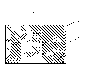
In Fig. 1, an insulating element is denoted by 1, comprising a
substrate element 2 made of a polymer, e.g. a polyolefin such as
polypropylene (PP) or polyethylene (PE), a polyamide such as
nylon-6 or nylon-6,6, polyurethane (PU), polystyrene (PS),
polyvinylchloride (PVC) or polyester such as polyethylene
terephthalate (PET). The substrate element may be a polymer film
having a thickness of 0.05 to 0.5 mm. The substrate element can,
however, also be configured as a self-supporting component
having a thickness of >3 mm. Furthermore, the substrate element
may comprise closed chambers. The substrate element comprises a
coating 3, preferably made of silver, on at least one side. The
silver coating has a thickness of <80 nm, in particular <50 nm,
preferably <30 nm.
Fig. 2 depicts a second exemplary embodiment, in which the
insulating element is configured as a honeycomb structure
CA 02833183 2013-10-15
element, its individual parts comprising two layers 4 and 5. The
first layer 4 is a layer having depressions in the form of
honeycomb cells 6 that are each open one side and whose edge
shape 7 in the layer plane 8 is as hexagonal as on the end of
the depression 6, i.e. on its base 9. The wall surfaces 10 of
the depressions 6 are substantially rectangular, preferably
trapezoidal, and substantially perpendicular, preferably
slightly inclined, relative to the layer plane 8. The second
layer 5 is a layer having depressions in the form of honeycomb
cells 11 that are each open one side and whose edge shape 12 in
the layer plane 13 is as hexagonal as on the end of the
depression 11, i.e. on its base 14. The wall surfaces 15 of the
depressions 11 are substantially rectangular, preferably
trapezoidal, and substantially perpendicular, preferably
slightly inclined, relative to the layer plane 13. The two sides
further comprise plane surfaces 16 and 17 at the front side and
plane surfaces 18 and 19 at the rear side. Rear side is to be
understood as that side in which, for instance, the deep-drawing
of a depression is performed, whereas front side is that side
which, for instance, remains unchangedly flat during deep-
drawing.
Moreover, Fig. 2 depicts a second embodiment with four layers
also by its individual parts. In addition to the two already
described layers, this exemplary embodiment further comprises
two flat layers 20 and 21. The metal coating according to the
invention can in this case be applied on the outer side of one
of the two layers 20 and 21, or on both layers 20 and 21.
Additionally or alternatively, the layers 4 and 5 may also be
provided with reflecting metal coatings.
Fig. 3 illustrates an assembled honeycomb structure element of
the second exemplary embodiment of Fig. 2, wherein the
depressions 6 and 11 of the two patterned layers 4 and 5 engage
CA 02833183 2013-10-15
11
each other in such a manner as to form closed honeycomb cells,
which are not visible in the Figure due to the chosen form of
representation, and are consequently not provided with reference
numerals, yet will be readily recognized in subsequent Figures.
The bases 9 and 14 of the unilaterally open honeycomb cells 6
and 11 contact the surfaces 18 and 19 that are plane at the rear
side, of the respectively oppositely located patterned layer.
The two flat layers 20 and 21 by contrast contact the surfaces
16 and 17 that are plane at the front side, of the respective,
patterned layer, thus closing the honeycomb cells 6 and 11,
which are open on one side. Except for the honeycomb cells
provided on the edges of the honeycomb structure element, all of
the honeycomb cells are thus closed in this exemplary
embodiment.
Fig. 4 depicts a detail of the exemplary embodiment of Fig. 3. A
single hexagonal honeycomb cell is shown in top view in Fig. 4a,
and two sectional views are represented in Fig. 4b along line B
and in Fig. 4c along line C, respectively, of Fig 4a. The
unilaterally open honeycomb cell on its end 11 has a hexagonal
base 14 and wall surfaces 15 substantially perpendicular,
preferably slightly inclined, thereto, which are substantially
rectangular, preferably trapezoidal.
Fig. 5 illustrates a portion of the exemplary embodiment
according to Fig. 3. Fig. 5a, in top view, depicts a patterned
layer of a honeycomb structure element having hexagonal
honeycomb cells, and Fig. 5b is a sectional view along line A-A
of Fig. 5a. The honeycomb cells, which are open on one side, of
the patterned layer have hexagonal bases 14 on their ends 11 and
wall surfaces 15 substantially perpendicular, preferably
slightly inclined, thereto. Furthermore, the patterned layer has
a plane surface 17 on its front side and a plane surface 19 on
its rear side. The side into which, for instance, the deep-
CA 02833183 2013-10-15
12
drawing of a depression is effected is referred to as rear side,
whereas the front side is that side which will, for instance,
remain unchangedly flat during deep-drawing. Fig. 5a, moreover,
indicates in broken lines where a closed honeycomb cell 22
having a hexagonal base is formed as a secondary structure as
two complementary, patterned layers are assembled.
Fig. 6 is a schematic top view of the honeycomb structure
element of Fig. 3, which comprises two assembled layers (4 and
5, analogously to the illustration in the preceding Figures)
providing honeycomb cells 6 having bases 9 and wall surfaces 10
as well as honeycomb cells 11 having bases 14 and wall surfaces
15 to form closed honeycomb cells 22 having bases 23, whose wall
surfaces each form half of the wall surfaces 10 of the honeycomb
cells 6 and wall surfaces 15 of the honeycomb cells 11. Assuming
that both the honeycomb cells 6 and the honeycomb cells 11 are
honeycomb cells that are open on one side, a honeycomb structure
element will be obtained, in which one third of the honeycomb
cells 22 are closed except for the edge regions of the honeycomb
structure element. In a further developed exemplary embodiment,
a honeycomb structure element in which all of the honeycomb
cells (6, 11 and 22) except those in edge regions are closed
will be obtained therefrom by providing appropriate cover
layers.
Fig. 7 illustrates a modified exemplary embodiment of a
honeycomb structure element, in which two further patterned
layers 24 and 25 are arranged between the two flat layers 20 and
21 in addition to the patterned layers 4 and 5 provided in Fig.
2, said two further patterned layers comprising depressions
formed by unilaterally open honeycomb cells 26 and 27 just as
the two patterned layers 4 and 5. The honeycomb cells 26 and 27
are arranged relative to one another just as the honeycomb cells
6 and 11 of the layers 4 and 5, respectively.
CA 02833183 2013-10-15
13
Figs. 8 and 9 depict insulating elements 28 that are assembled
to form an insulating container 29. These may be insulating
elements according to any one of the previously described
exemplary embodiments, e.g. an insulating element according to
Fig. 1, according to Figs. 2-6, or according to Fig. 7. From the
exploded view according to Fig. 8, it is apparent that each of
the container walls of the parallelepiped-shaped container is
formed by an insulating element 28. The insulating container
according to the invention may, however, have any desired shape
and, for instance, also be spherical, pyramid-shaped etc.
Fig. 10 depicts the cross section of an insulating container 31
whose internal elements 30, which completely surround the
cooling space 33, are filled with PCM devices. These elements 30
filled with PCM devices can be realized as independent modules
or part of an insulating element or insulating container. The
elements 30 may, for instance, be insulating elements according
to Figs. 2-7, whose honeycomb cells are filled with PCM devices.
The insulating container 31 comprises a shell 32 which is, for
instance, composed of wall elements to whose inner sides an
insulating element 30 is each attached.
In all of the previously described exemplary embodiments, the
honeycomb cells may comprise gas fillings. Gases to be
considered include, for instance, a gas having a thermal
conductivity of <22 mWm-1K-1, such as, in particular, noble gases,
e.g. xenon, krypton or argon. Within the honeycomb cells,
subatmospheric pressure is preferably maintained. The gas
pressure within the cells is preferably 100 - 700 mbar.