Note : Les descriptions sont présentées dans la langue officielle dans laquelle elles ont été soumises.
CA 02 83 94 7 6 2 01 3 -1 2 -1 6
CA Application
Makes Ref: 10798/00002
1 AUDIO SIGNAL ADAPTER DEVICE
2 FIELD
3 The present invention generally relates to an electronic technical field,
and more particularly
4 relates to an audio signal adapter device.
BACKGROUND
6 With the development of an audio signal coding/decoding technology, more
and more
7 electronic equipments transmitting data via an audio interface are
produced. For example, the
8 electronic equipment may be connected with a mobile communication device
(such as a mobile
9 phone) via a headphone plug of the mobile communication device for
receiving an audio signal
output from the mobile communication device.
11 As an output power of the headphone plug is usually very low, except the
electronic
12 equipment (such as a headphone) with low power consumption, the
electronic equipment
13 receiving the audio signal via the headphone plug generally needs to use
an external power
14 source or an internal battery for normal working, which increases a cost
of the electronic
equipment and enlarges a size of the electronic equipment.
16 SUMMARY
17 The present disclosure overcomes the defects of the prior art, and
provides an audio signal
18 adapter device which can realizes a feeding function via an audio
signal.
19 The present disclosure provides an audio signal adapter device,
comprising an input
interface, an output interface, a boosting unit, a rectifying unit and a
filtering unit.
21 The input interface comprises at least one audio pin configured to
receive an audio signal
22 output from an audio signal sending device. The at least one audio pin
of the input interface
23 outputs the audio signal to an input end of the boosting unit.
24 The boosting unit is configured to boost a voltage of the audio signal,
and to output a
boosted audio signal to an input end of the rectifying unit via an output end
thereof,
26 The rectifying unit is configured to rectify the boosted audio signal to
obtain a rectified level,
27 and to output the rectified level to an input end of the filtering unit
via an output end thereof.
28 The filtering unit is configured to filter the rectified level to obtain
a direct current level, and
29 to output the direct current level to a power pin of the output
interface via output end thereof.
1
22484207.1
CA 02 83 94 7 6 2 01 3-1 2-1 6
CA Application
Blakes Ref: 10798/00002
The output interface further comprises an audio signal pin, the audio signal
pin is
2 connected with the at least one audio pin of the input interface or the
output end of the boosting
3 unit,
4 The output interface further comprises a reference signal pin, the input
interface further
comprises a ground pin, and the reference signal pin is connected with the
ground pin.
6 Furthermore, the boosting unit is a boosting transformer, and the
boosting transformer
7 comprises a primary coil and a secondary coil.
8 A first pin of the primary coil is used as the input end of the boosting
unit to be connected
9 with the at least one audio pin, and a second pin of the primary coil is
grounded.
At least one output pin of the secondary coil is used as the output end of the
boosting unit
11 to be connected with the input end of the rectifying unit, and a tap of
the secondary coil is
12 grounded.
13 Furthermore, the rectifying unit comprises at least one diode, an anode
of the at least one
14 diode is connected with the input end of the rectifying unit, and a
cathode of the at least one
diode is connected with the output end of the rectifying unit.
16 Furthermore, the secondary coil of the boosting transformer comprises
two output pins, and
17 the input end of the rectifying unit comprises two input pins.
18 The two output pins of the secondary coil are connected with the two
input pins of the
19 rectifying unit respectively;
The rectifying unit comprises two diodes, and anodes of the two diodes are
connected with
21 the two input pins of the rectifying unit respectively.
22 Furthermore, the filtering unit comprises a capacitor.
23 A first end of the capacitor is connected with the input end or the
output end of the rectifying
24 unit.
The input end of the rectifying unit is connected with the output end of the
rectifying unit.
26 Furthermore, the boosting unit is a boosting transformer, and the
boosting transformer
27 comprises a primary coil and a secondary coil.
28 A first pin of the primary coil is used as the input end of the boosting
unit to connected with
29 the at least one audio pin, and a second pin of the primary coil is
grounded.
2
22484207.1
CA 0283 9476 2013-12-16
CA Application
Makes Ref: 10798/00002
1 A first output pin of the secondary coil is used as the output end of the
boosting unit to be
2 connected with the input end of the rectifying unit, and a second output
pin of the secondary coil
3 is grounded.
4 Furthermore, the rectifying unit comprises one diode, an anode of the
diode is connected
with the input end of the rectifying unit, and a cathode of the diode is
connected with the output
6 end of the rectifying unit.
7 Furthermore, the second pin of the primary coil is connected with the
ground pin of the
8 input interface.
9 Furthermore, the output interface is a USB output interface.
The power pin is a VBUS pin of the USB output interface.
11 The audio signal pin is one of a D+ pin and a D- pin of the USB output
interface, and the
12 reference signal pin is the other one of the D+ pin and the D- pin of
the USB output interface.
13 Furthermore, the first pin of the primary coil is connected with the at
least one audio pin via
14 a resistor.
Furthermore, the input interface comprises two audio pins: a left-channel pin
and a
16 right-channel pin.
17 Furthermore, one of the left-channel pin and the right-channel pin is
configured to output
18 the audio signal to the input end of the boosting unit, and the other
one of the left-channel pin
19 and the right-channel pin is configured to be connected with the audio
signal pin of the output
interface.
21 In conclusion, the present disclosure realizes a feeding function via
the audio signal with a
22 low hardware cost. When the electronic equipment is used together with
the audio signal
23 adapter device (such as an audio cable) according to the present
disclosure, it can obtain
24 electric energy while receiving the audio signal, thus reducing a cost
of the electronic equipment
and decreasing a size of the electronic equipment.
26 Furthermore, the audio signal adapter device according to the present
disclosure may
27 further comprise a USB plug, and thus it can be inserted into a USB
socket of the electronic
28 equipment (an audio signal receiving device), then the electronic
equipment can obtain power
29 via the VBUS pin and can use one of the D+ pin and the D- pin as the
audio signal pin (the pin
corresponding to a left-channel audio signal, a right-channel audio signal, a
mono audio signal
3
22484207.1
CA 02 83 94 7 6 2 01 3-1 2-1 6
CA Application
Blakes Ref 10798/00002
1 or a hybrid channel audio signal) and use the other one of the D+ pin and
the 0- pin as the
2 ground pin (or referred to as the reference signal pin), so as to receive
the audio signal output
3 from a headphone jack of an audio signal sending device.
4 BRIEF DESCRIPTION OF THE DRAWINGS
Fig. 1 is a schematic diagram of an audio adapter device according to a first
embodiment of
6 the present disclosure;
7 Fig. 1 a shows a schematic diagram of an audio signal receiving module in
an audio signal
8 receiving device connected with the audio signal adapter device according
to the first
9 embodiment of the present disclosure, in which the audio signal receiving
module is configured
to receive a differential signal;
11 Fig. 2 is a schematic diagram of a variation of the audio signal adapter
device according to
12 the first embodiment of the present disclosure, in which the D+ pin and
the 0- pin are
13 exchanged relative to the D+ pin and the D- pin shown in Fig. 1;
14 Fig. 3 is a schematic diagram of a variation of the audio signal adapter
device according to
the first embodiment of the present disclosure, in which a left-channel pin is
connected with a
16 primary coil of a boosting transformer, and a right-channel pin is only
connected with the D+ pin;
17 Fig. 4 is a schematic diagram of an audio signal adapter device
according to a second
18 embodiment of the present disclosure;
19 Fig. 5 is a schematic diagram of an audio signal adapter device
according to an
embodiment of the present disclosure, in which an audio signal pin is
connected with an output
21 pin of a boosting transformer;
22 Fig. 6 is a schematic diagram of an audio signal adapter device
according to an
23 embodiment of the present disclosure, in which an output interface of
the audio signal adapter
24 device is replaced by other types of interfaces having a power pin, an
audio signal pin, a
reference signal pin, and a ground pin.
26 DETAILED DESCRIPTION
27 In the following, the present disclosure will be described in detail
with reference to drawings
28 and embodiments.
29 The audio signal adapter device in the present disclosure may be an
audio cable, an audio
adapter cable or an audio adapter.
4
22484207.1
CA 02 83 94 7 6 2 01 3-1 2-1 6
CAApplicatton
Blakes Ref. 10798/00002
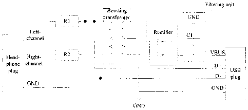
1 FIRST EMBODIMENT
2 Fig. 1 is a schematic diagram of an audio signal adapter device according
to a first
3 embodiment of the present disclosure. As shown in Fig. 1, the audio
signal adapter device
4 comprises a headphone plug, a boosting unit (such as a boosting
transformer shown in Fig. 1),
a rectifying unit (such as a rectifier shown in Fig. 1), a filtering unit and
a USB plug.
6 The headphone plug is configured to be connected with a headphone jack of
an audio
7 signal sending device (such as a mobile phone) and to receive an audio
signal output from the
8 audio signal sending device.
9 The headphone plug comprises a left-channel pin, a right-channel pin and
a ground pin.
The left-channel pin and the right-channel pin are connected with a same pin
of a primary
11 coil of the boosting transformer, and the ground pin of the headphone
plug is connected with the
12 other pin of the primary coil of the boosting transformer.
13 Alternatively, in order to reduce the power consumption of the audio
signal sending device,
14 a resistor R1 may be connected in series between the left-channel pin
and the boosting
transformer, and a resistor R2 may be connected in series between the right-
channel pin and
16 the boosting transformer. In this embodiment, a resistance of the
resistor R1 is equal to that of
17 the resistor R2.
18 Furthermore, the ground pin of the headphone plug is also connected with
the D- pin of the
19 USB plug.
The boosting transformer, comprising a primary coil and a secondary coil, is
configured to
21 boost an input voltage (generally about 1V) at an input end (the primary
coil) to an output
22 voltage (for example, greater than or equal to 5V) at an output end (the
secondary coil).
23 As described above, the primary coil of the boosting transformer
comprises two pins, one
24 pin is connected with the left-channel pin and the right-channel pin of
the headphone plug
respectively, and the other pin is connected with the ground pin of the
headphone plug.
26 The secondary coil of the boosting transformer comprises two output pins
and one tag, the
27 two output pins are connected with the two input pins of an input end in
the rectifier respectively,
28 and the tag is connected with the ground pin of the USB plug.
29 The rectifier is configured to rectify an alternating current level
input from the input end to
obtain a rectified level, and to output the rectified level via an output end.
5
22484207.1
CA 02839476 2013-12-16
CA Application
Blakes Ref: 10798/00002
1 In this embodiment, the rectifier comprises two input pins of the input
end and one output
2 pin of the output end. Correspondingly, the rectifier comprises two
diodes, anodes of the two
3 diodes are connected with the two input pins of the rectifier
respectively, and cathodes of the
4 two diodes are connected with the output pin of the rectifier.
The filtering unit, comprising an input end and an input end, is configured to
convert the
6 rectified level input from the input end into a smooth direct current
level and to output the
7 smooth direct current level via the output end.
8 In this embodiment, the input end of the filtering unit is connected with
the output end of the
9 rectifier, and the output end of the filtering unit is connected with the
VBUS pin (the power pin)
of the USB plug, thus the electronic equipment connected with the USB plug is
supplied with
11 power via the VBUS pin.
12 In this embodiment, the input end of the filtering unit is connected
with the output end of the
13 filtering unit. The filtering unit further comprises a capacitor Cl. One
end of the capacitor Cl is
14 connected with the input/output end, and the other end of the capacitor
Cl is grounded.
Furthermore, the left-channel pin and the right-channel pin of the headphone
plug are also
16 connected with the D+ pin of the USB plug.
17 When the audio signal adapter device according to the first embodiment
of the present
18 disclosure is used together with an electronic equipment, the headphone
plug of the audio
19 signal adapter device may be inserted into a headphone jack of an audio
signal sending device
(such as the mobile phone), and the USB plug of the audio signal adapter
device may be
21 inserted into the USB socket of the electronic equipment. Such that, the
electronic equipment
22 can obtain power via the VBUS pin of the USB plug/socket (collectively
known as the USB
23 output interface), meanwhile, use the D+ pin as the audio signal pin and
use the D- pin as the
24 reference signal pin so as to receive the audio signal output from the
headphone jack of the
audio signal sending device.
26 Furthermore, Fig. la shows a schematic diagram of an audio signal
receiving module in an
27 audio signal receiving device connected with the audio signal adapter
device according to the
28 first embodiment of the present disclosure. The audio signal receiving
module is configured to
29 receive a differential signal.
As shown in Fig. 1 a, the audio signal receiving module comprises a
comparator, a positive
31 terminal of the comparator is connected with the D+ pin of the USB plug,
a negative terminal of
6
22484207.1
CA 02 83 94 7 6 2 01 3-1 2-1 6
CA Application
Makes Ref 10798/00002
1 the comparator is connected with the D- pin of the USB plug, a ground pin
of the comparator is
2 grounded, a power pin of the comparator is connected with a power supply,
and an output pin of
3 the comparator is configured to output a square wave corresponding to the
input audio signal.
4 Alternatively, the positive terminal of the comparator may be connected
with the D- pin of the
USB plug, and the negative terminal of the comparator may be connected with
the D+ pin of the
6 USB plug.
7 According to the basic principle of the present disclosure, many
alternatives and
8 modifications may be made to the above embodiments as follows,
9 As shown in Fig. 2, in other embodiments of the present disclosure, it is
also possible to
use the D- pin of the USB output interface as the audio signal pin, and to use
the D+ pin of the
11 USB output interface as the reference signal pin.
12 As shown in Fig. 3, in other embodiments of the present disclosure, it
is also possible to
13 connect only one audio pin (for example, the left-channel pin) of the
headphone plug with the
14 primary coil of the boosting transformer, and to connect the other audio
pin (for example, the
right-channel pin) of the headphone plug with only the D+ pin of the USB plug.
16 Certainly, when the electronic equipment only needs to receive the audio
data of one
17 channel (for example, the left channel), it is also possible for the
audio signal adapter device
18 shown in Fig. 3 not to use the right-channel pin.
19 SECOND EMBODIMENT
Fig. 4 is a schematic diagram of an audio signal adapter device according to a
second
21 embodiment of the present disclosure. As shown in Fig. 4, the
differences between the second
22 embodiment and the first embodiment are as follows.
23 In this embodiment, only one output pin of the secondary coil of the
boosting transformer is
24 connected with the input pin of the rectifier, thus the rectifier only
has to comprise one input pin
and one diode.
26 Apparently, compared with the first embodiment, a half of electric
energy of the secondary
27 coil of the boosting transformer will be lost if using the audio signal
adapter device in the second
28 embodiment. However, a circuit structure of the audio signal adapter is
simplified, thus a
29 hardware cost is reduced.
7
22484207 1
CA 02839476 2013-12-16
CA Application
Blakes Ref. 10798/00002
1 In this embodiment, the other output pin of the secondary coil of the
boosting transformer is
2 grounded, and the boosting transformer does not comprise a tag.
3 The above embodiments of the present disclosure realize a feeding
function via the audio
4 signal with a low hardware cost. When the electronic equipment is used
together with the audio
signal adapter device (such as an audio cable) according to the present
disclosure, it can obtain
6 electric energy while receiving the audio signal, thus reducing a cost of
the electronic equipment
7 and decreasing a size of the electronic equipment.
8 Furthermore, since the audio signal adapter device according to the
present disclosure
9 comprises the USB plug, it can be inserted into the USB socket of the
electronic equipment (the
audio signal receiving device), and then the electronic equipment can obtain
power via the
11 VBUS pin and can use one of the D+ pin and the D- pin as the audio
signal pin (the pin
12 corresponding to a left-channel audio signal, a right-channel audio
signal, a mono audio signal
13 or a hybrid channel audio signal) and use the other one of the D+ pin
and the D- pin as the
14 ground pin (or referred to as the reference signal pin) so as to receive
the audio signal output
from the headphone jack of the audio signal sending device.
16 Certainly, according to the basic principle of the present disclosure,
the headphone plug in
17 the above embodiments may be replaced with other types of input
interfaces having an audio
18 pin (a left-channel pin, a right-channel pin and/or a mono pin) and a
reference signal pin (a
19 ground pin).
Furthermore, as shown in Fig. 6, the USB plug in the above embodiments may be
replaced
21 with other types of output interfaces having a power pin, an audio
signal pin, a reference signal
22 pin and a ground pin.
23 Furthermore, the output interface of the above embodiments may comprise
two output
24 interfaces, which are a power output interface (may comprise a power pin
and a ground pin) and
an audio signal output interface (may comprise an audio signal pin and a
reference signal pin).
26 Furthermore, the above input interface may be fixed connected with the
audio signal
27 sending device.
28 Furthermore, the above output interface may be fixed connected with the
electronic
29 equipment (the audio signal receiving device).
8
22484207,1
CA 02 83 947 6 2 01 3-1 2-1 6
CAApplication
Bakes Ref. 10798/00002
1 The above input interface may comprise a plurality of plugs, such as an
audio signal plug
2 having an audio signal input pin and a MIC plug having a M1C pin.
3 Furthermore, as shown in Fig. 5, the audio signal pin of the output
interface may be
4 connected with the output pin of the boosting transformer for outputting
the audio signal.
9
22484207.1