Note : Les descriptions sont présentées dans la langue officielle dans laquelle elles ont été soumises.
CA 02852646 2014-04-16
WO 2013/056356
PCT/CA2012/000971
1
Ripple Cancellation Converter with High Power Factor
Field
This invention relates to methods and circuits for improving the performance
of an
AC to DC power supply. In particular, methods and circuits are provided for
power supplies
that achieve high power factor (PF) at the AC side and at the same time,
reduce or
substantially eliminate ripple in the DC output power. The methods and
circuits may be used
in any application where high power factor and/or low output ripple are
required. In
particular, the methods and circuits may be used in DC lighting applications,
such as in light
emitting diode (LED) lighting, wherein suppression of low frequency ripple in
the output
power eliminates visible flickering.
Background
Regulation concerning power factor correction for a wide range of devices is
becoming increasingly stringent. For example, new regulation requires power
factor
correction for any light emitting diode (LED) power supply with output power
higher than
For low to medium power level (e.g., 5 W to 100 W), a flyback converter is
often
used. Figure 1 shows a block diagram of such a system. By forcing the average
input current
to follow the input voltage, high power factor can be achieved. In order to
reduce the cost,
critical conduction mode is often used to achieve power factor correction.
However, this
results in a ripple in the output voltage at harmonics of the line frequency.
The second
harmonic (e.g., 120 Hz for North America or 100 Hz for China, Europe) is of
particular
concern for DC lighting applications, such as LED lighting, as it results in
visible flickering
wherein the human eye can see fluctuation of the light emitting from the LED.
In such a conventional design there is a compromise between power factor and
small
low frequency current ripple through the load. For example, in order to
achieve a power
factor higher than 90%, the peak to peak value of the load current ripple can
be as high as
60% of the average DC value. For example, for an average load current of 0.5
A, the low
frequency current ripple can be as high as 0.3 A (peak to peak). This raises
several problems:
Firstly, as mentioned above, for DC lighting (e.g., LED) applications, the
ripple current
CA 02852646 2014-04-16
WO 2013/056356 PCT/CA2012/000971
2
causes visible flickering. Secondly, it is difficult to achieve variable
output power. When the
average load current is reduced, the ripple current does not decrease
proportionally and
therefore the ripple current will become more of a problem at reduced output
power. In DC
lighting applications, flickering will be worse at reduced brightness.
Thirdly, the ripple
current degrades the lifespan of many devices, such as LEDs.
To achieve high power factor and small low frequency current ripple, two-stage
conversion may be used. Figure 2 shows a circuit block diagram of a
conventional converter
used to drive an LED, where the first stage 20 is typically a boost converter
that converts the
AC voltage into a high voltage, e.g., 400 V, and also achieves power factor
correction. The
second stage 22 is a DC to DC converter that converts the 400 V into a lower
voltage
required by the load 100, e.g., 50 V or 125 V, provides electrical isolation,
and regulates the
load current. However, compared to the converter of Figure 1, the converter of
Figure 2
suffers from the drawbacks of higher cost and larger size.
Summary
Provided herein is a circuit for use with a power supply that provides a main
output
including a main DC voltage with a first AC voltage ripple or a main DC
current with a first
AC current ripple, the circuit comprising a ripple cancellation converter
that: (i) provides a
second AC voltage ripple and is connected in series with the main output, such
that the first
AC voltage ripple is substantially cancelled; or (ii) provides a second AC
current ripple and is
connected in parallel with the main output, such that the first AC current
ripple is
substantially cancelled; wherein substantially ripple-free DC output power is
provided.
Also provided herein is a circuit that provides DC power, comprising: a
portion that
outputs a main DC voltage with a first AC voltage ripple or a main DC current
with a first
AC current ripple; and a ripple cancellation converter that: (i) provides a
second AC voltage
ripple and is connected in series with the main output, such that the first AC
voltage ripple is
substantially cancelled; or (ii) provides a second AC current ripple and is
connected in
parallel with the main output, such that the first AC current ripple is
substantially cancelled;
wherein substantially ripple-free DC output power is provided.
In some embodiments, the ripple cancellation converter provides an auxiliary
output
comprising: (i) an auxiliary DC voltage with the second AC voltage ripple,
wherein the
second AC voltage ripple is substantially equal in magnitude and substantially
opposite in
CA 02852646 2014-04-16
WO 2013/056356 PCT/CA2012/000971
3
phase to the first AC voltage ripple; or (ii) an auxiliary DC current with the
second AC
current ripple, wherein the second AC current ripple is substantially equal in
magnitude and
substantially opposite in phase to the first first AC current ripple; wherein
the main output
and the auxiliary output are combined such that: (i) a total DC voltage or a
total DC current is
provided; (ii) the second AC voltage ripple substantially cancels the first AC
voltage ripple,
or the second AC current ripple substantially cancels the first AC current
ripple; (iii) the total
DC voltage or the total DC current is substantially ripple-free. The ripple
cancellation
converter may comprise a buck converter, a boost converter, a buck-boost
converter, or a full
bridge converter.
In one embodiment, the circuit further comprises a sensor that senses the
first AC
voltage ripple or the first AC current ripple, and outputs a sensor signal to
the ripple
cancellation converter. In one embodiment, the circuit further comprises a
power factor
correction portion. Operation of the power factor correction portion may be
based on a
feedback signal derived from a load current.
In some embodiments, the substantially ripple-free DC output power is
variable.
Embodiments may be used with an AC-DC power supply. In one embodiment, the
portion that outputs a main DC voltage with a first AC voltage ripple or a
main DC current
with a first AC current ripple comprises an AC-DC power supply. The AC-DC
power supply
may comprise a flyback converter, an isolated boost converter, a buck-boost
converter, a
buck converter, or a boost converter.
In some embodiments, a load comprises an LED.
Also provided herein is a method for providing DC power from a main output
power
comprising a main DC voltage with a first AC voltage ripple or a main DC
current with a first
AC current ripple, the method comprising: (i) connecting a second AC voltage
ripple in series
with the main output power, such that the first AC voltage ripple is
substantially cancelled; or
(ii) connecting a second AC current ripple in parallel with the main output,
such that the first
AC current ripple is substantially cancelled; wherein substantially ripple-
free DC output
power is provided.
Also provided herein is a method for providing DC power, comprising:
outputting a
main output power comprising a main DC voltage with a first AC voltage ripple
or a main
DC current with a first AC current ripple; and (i) connecting a second AC
voltage ripple in
series with the main output power, such that the first AC voltage ripple is
substantially
CA 02852646 2014-04-16
WO 2013/056356 PCT/CA2012/000971
4
cancelled; or (ii) connecting a second AC current ripple in parallel with the
main output, such
that the first AC current ripple is substantially cancelled; wherein
substantially ripple-free DC
output power is provided.
In some embodiments the method further comprises: (i) providing an auxiliary
DC
voltage with the second AC voltage ripple, wherein the second AC voltage
ripple is
substantially equal in magnitude and substantially opposite in phase to the
first AC voltage
ripple; or (ii) providing an auxiliary DC current with the second AC current
ripple, wherein
the second AC current ripple is substantially equal in magnitude and
substantially opposite in
phase to the first first AC current ripple; wherein connecting includes
combining the auxiliary
DC voltage with the main DC voltage, or combining the main DC current with the
auxiliary
DC current, such that: (i) a total DC voltage or a total DC current is
provided; (ii) the second
AC voltage ripple substantially cancels the first AC voltage ripple, or the
second AC current
ripple substantially cancels the first AC current ripple; (iii) the total DC
voltage or the total
DC current is substantially ripple-free.
Embodiments may include using a buck converter, a boost converter, a buck-
boost
converter, or a full bridge converter to provide the second AC voltage ripple
or to provide the
second AC current ripple.
One embodiment further comprises sensing the first AC voltage ripple or the
first AC
current ripple, and outputting a sensor signal to the ripple cancellation
converter.
Another embodiment further comprises adjusting a power factor of a circuit
used to
provide DC power. The method may comprise adjusting the power factor based on
a
feedback signal derived from a load current.
Embodiments may include varying the substantially ripple-free DC output power.
Embodiments may be used with an AC-DC power supply. Various embodiments
include using a flyback converter, an isolated boost converter, a buck-boost
converter, a buck
converter, or a boost converter for the AC-DC power supply.
Brief Description of the Drawings
For a better understanding of the invention, and to show more clearly how it
may be
carried into effect, embodiments will be described, by way of example, with
reference to the
accompanying drawings, wherein:
CA 02852646 2014-04-16
WO 2013/056356 PCT/CA2012/000971
Figure 1 is a block diagram of an LED driver with a flyback converter
according to
the prior art;
Figure 2 is a block diagram of a two-stage LED driver according to the prior
art;
Figure 3 is a block diagram of a power supply with a ripple cancellation
controller
according to one embodiment;
Figure 4 is a block diagram of a power supply with a ripple cancellation
controller
and control architecture, according to one embodiment;
Figure 5 is a plot showing voltage waveforms of the embodiment of Figure 4;
Figure 6 is a block diagram of a power supply with a ripple cancellation
controller
and load current control according to one embodiment;
Figure 7 is a block diagram of apower supply with a ripple cancellation
controller
based on an isolated boost converter, according to one embodiment;
Figure 8 is a diagram of power supply with a ripple cancellation controller
based on a
non-isolated buck-boost converter that generates output Vol, according to one
embodiment;
Figure 9 is a schematic diagram of power supply with a ripple cancellation
controller
based on a full bridge converter and pulse width modulation control, according
to one
embodiment;
Figure 10 is a schematic diagram of a ripple cancellation converter
implemented with
a buck converter, according to one embodiment;
Figure 11(a) is a schematic diagram of a ripple cancellation converter
implemented
with a buck-boost converter, according to one embodiment;
Figure 11(b) is a diagram of a power supply with current control using a
second
primary winding for isolation, according to one embodiment;
Figure 12 is a block diagram of a power supply with current control and an
external
DC reference voltage, according to one embodiment;
Figure 13 is a block diagram of driver power supply with a parallel-connected
ripple
current cancellation controller and load current control, according to one
embodiment;
Figure 14 is a schematic diagram of driver power supply secondary side and
control
circuitry suitable for integrated circuit implementation, according to one
embodiment;
CA 02852646 2014-04-16
WO 2013/056356 PCT/CA2012/000971
6
Figure 15(a) is a schematic diagram of driver power supply secondary side and
control circuitry suitable for integrated circuit implementation, according to
another
embodiment;
Figure 15(b) is a schematic diagram of driver power supply secondary side and
control circuitry suitable for integrated circuit implementation based on the
embodiment of
Figure 14(a), wherein an opto-coupler is not used;
Figure 16 is a schematic diagram of driver power supply secondary side and
control
circuitry suitable for integrated circuit implementation, wherein load current
control is
achieved by applying a voltage to a current amplifier;
Figure 17 is a schematic diagram of driver power supply secondary side and
control
circuitry based on a buck-boost converter, suitable for integrated circuit
implementation,
according to another embodiment;
Figure 18 is a schematic diagram of driver power supply secondary side
suitable for
implementation using discrete components, according to one embodiment;
Figure 19 is a block diagram showing driver power supply secondary side at
least
partially implemented in an integrated circuit, wherein the DC reference
voltage is inside the
integrated circuit, according to one embodiment;
Figure 20 is a block diagram of an embodiment with variable output power,
wherein
LED dimming control is provided by using an on/off control signal for the
ripple cancellation
converter;
Figure 21 is a schematic diagram of a power supply with variable output power
wherein a buck converter is used for the ripple cancellation converter,
according to one
embodiment;
Figure 22 is a plot showing a control signal (top) and load current (bottom)
for the
embodiment of Figure 21;
Figure 23 is a block diagram of a test setup used to evaluate performance of a
power
supply with a ripple cancellation converter according to one embodiment;
Figure 24 is a plot showing performance for the test setup of Figure 23,
wherein the
upper waveform is the DC coupled load current (200 mA/div), the middle
waveform is the
AC coupled load current (10 mA/div), and the bottom waveform is the AC ripple
voltage at
the main output, between Vol+ and Vol- (2 V/div); and
CA 02852646 2014-04-16
WO 2013/056356 PCT/CA2012/000971
7
Figure 25 is a plot of the AC input current waveform at 110 V AC and 50 V, 0.7
A
output, for the test setup of Figure 23.
Detailed Description
Provided herein are AC to DC power supply methods and circuits that provide
substantially ripple-free output power and achieve high power factor. The
methods and
circuits provided herein may be used in any power supply application where
substantially
ripple-free output power and high power factor are desirable, such as, but not
limited to,
computers, tablets, cell phones, etc. Embodiments are described primarily with
respect to
lighting applications, e.g., wherein the load is an LED; however, it is to be
understood that
they are not limited thereto.
For the sake of brevity, the term "LED" as used herein is intended to refer to
a single
LED or to multiple LEDs electrically connected together (e.g., in a series,
parallel, or series-
parallel arrangement). It will be appreciated that an LED lighting fixture
(e.g., an LED lamp)
may include a single LED or multiple LEDs electrically connected together.
The methods and circuits achieve high power factor (PF) at the AC side and
reduce or
substantially eliminate ripple in the DC output power. The ripple may be a
harmonic of the
line frequency, such as the second harmonic (e.g., 120 Hz for North America or
100 Hz for
China, Europe) of the line frequency. In DC lighting (e.g., LED) applications,
ripple at the
2' harmonic results in visible flickering, wherein the human eye can see
fluctuation of the
light emitting from the LED. Therefore, of particular interest for lighting
applications is
suppression or elimination of ripple at the 2nd harmonic. The methods and
circuits described
herein reduce or substantially eliminate ripple at the second harmonic and at
other harmonics.
The methods and circuits provided herein minimize component counts, providing
power
supplies that are compact and cost effective. Embodiments may be implemented
in any
currently-available semiconductor technology. Embodiments may be implemented
as a
hybrid circuit comprising one or more integrated circuit (IC) component
together with
discrete components, or substantially as an IC.
Provided herein are circuits and methods for use with a power supply that
provides a
main output including a main DC voltage having a first AC voltage ripple, or a
main DC
current having a first AC current ripple. The methods and circuits include a
ripple
cancellation converter (RCC). The ripple cancellation converter (i) provides a
second AC
CA 02852646 2014-04-16
WO 2013/056356 PCT/CA2012/000971
8
voltage ripple connected in series with the main output, such that the first
AC voltage ripple
is substantially cancelled; or (ii) provides a second AC current ripple
connected in parallel
with the main output, such that the first AC current ripple is substantially
cancelled. As a
result, substantially ripple-free DC output power is provided.
In some embodiments, a first portion provides most of the DC power (i.e., the
main
output power) to the load with a small AC component (i.e., a selected amount
of voltage
ripple or current ripple), and a second portion provides a small amount of DC
power (i.e.,
auxiliary power) to the load and an AC component that cancels the voltage
ripple or current
ripple produced by the first portion. The AC component provided by the second
portion is
substantially equal in magnitude and substantially opposite in phase (i.e.,
inverse) to the AC
component provided by the first portion, such that combining the AC components
of the first
and second portions substantially cancels ripple in the total output power to
the load. The
total output power to the load therefore includes the main DC power provided
by the first
portion together with the auxiliary DC power provided by the second portion,
substantially
without ripple. The first portion may be implemented with fewer and/or smaller
components,
such as, for example, a smaller output capacitor, such that size and cost of
the first portion is
reduced, and efficiency is improved. Also, since the auxiliary power provided
by the second
portion is only a small amount of the total output power, it may be
implemented using
passive components with smaller inductance and capacitance values, and active
components
with lower voltage and/or current ratings, so as to achieve ripple
cancellation and supply the
required auxiliary output power with reduced cost and size relative to a
conventional
converter such as shown in Figure 2. Power supply methods and circuits
provided herein
include series-connected embodiments for voltage ripple cancellation, wherein
the output of a
ripple cancellation converter is connected in series with a main output, and
parallel-connected
embodiments for current ripple cancellation, wherein the output of a ripple
cancellation
converter is connected in parallel with a main output.
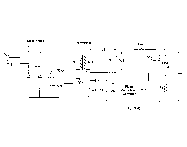
Series Ripple Cancellation Converter
A series-connected embodiment based on a flyback converter will now be
described
with reference to Figure 3. In the embodiment of Figure 3, the primary side
includes a full-
wave bridge rectifier and a switch S in series with a transformer primary
winding Np. A
power factor correction (PFC) controller controls the switch S to achieve high
power factor at
CA 02852646 2014-04-16
WO 2013/056356 PCT/CA2012/000971
9
the primary (input) side. Different from the conventional flyback architecture
shown in
Figure 1, the secondary side includes first and second secondary windings Nsl
and Ns2,
respectively. Winding Nsl provides the main voltage Vol. Winding Ns2 provides
a
secondary voltage Vo2. The voltage Vo2 is followed by a ripple cancellation
converter 35
with auxiliary output voltage Vo3. The main voltage Vol and the auxiliary
voltage Vo3 are
connected in series to provide the total output voltage Vout for the load 100.
When power factor correction is achieved, or when the power factor is high,
the
output voltage Vol will contain a significant amount of low frequency voltage
ripple at a
frequency two times the line frequency (e.g., 120 Hz in North America), as
shown in the
following equation:
Vol = Vo 1 _dc + Vol_rip (1)
In the above equation, Vol_dc represents the DC component of Vol and Vol_rip
represents the low frequency component of Vol.
The output of the ripple cancellation converter may be expressed by the
following
equation:
Vo3 = Vo3_dc + Vo3_rip (2)
In the above equation, Vo3_dc represents the DC component of Vo3, and Vo3_rip
represents the low frequency component of Vo3.
Therefore, the total output voltage which will be applied to the load may be
derived
as:
Vout = Vol + Vo3 = Vo 1 _dc + Vo3_dc + Vol_rip + Vo3_rip (3)
The DC value (Vout_dc) and low frequency ripple value (Vout_rip) of the total
output
Vout may be expressed as:
Vout dc = Vol dc + Vo3_dc (4)
Vout_rip = Vol_rip + Vo3_rip (5)
The ripple cancellation converter is constructed and controlled such that the
low
frequency voltage ripple (Vo3_rip) is the same in magnitude and inverse in
phase compared
with the low frequency voltage ripple in Vol, as shown in the following
equation:
Vo3_rip = - Vol_rip (6)
CA 02852646 2014-04-16
WO 2013/056356 PCT/CA2012/000971
Substituting (6) into (5), the following equation is obtained:
Vout_rip = 0 (7)
Therefore, the voltage across the load will contain substantially no low
frequency
ripple. In the case where the load is an LED, flickering of the LED is avoided
and lifespan of
the LED is not degraded.
Figure 4 shows a block diagram of a series embodiment with control blocks. In
the
figure, a Vol ripple sensor 40 senses the low frequency ripple component of
Vol and
provides an output of the ripple with inverse polarity to a RCC control
circuit 37. The Vol
ripple sensor may include, for example, a high pass filter. The Vol ripple
sensor output is ¨
Vol_rip. Vo3_dc_ref is a reference voltage for the DC value of the RCC output
voltage.
The reference of the RCC is Vo3 ref= Vo3_dc_ref + (- Vol_rip). Therefore, the
control
circuit 37 will regulate the output voltage Vo3 as:
Vo3 = Vo3 dc ref + (- Vol _rip) = Vo3 dc ref ¨ Vol _rip (8)
Therefore, the output voltage Vout may be expressed as:
Vout = Vol dc + Vol_rip + Vo3 _ dc_ ref ¨ Vol_rip = Vo 1 dc + Vo3 dc (9)
In the above equation, Vo3_dc = Vo3_dc_ref. The value of Vol_dc may be
regulated
by the PFC controller 30 to control the DC value of the load current. This is
discussed in
detail below.
Whereas it may be desirable to reduce the power consumption, and therefore
size, of
the ripple cancellation converter, the DC value of Vo3 (Vo3_dc) should be
minimized. For
example, the value of Vo3_dc_ref may be set to 0, in which case the output
voltage of the
ripple cancellation converter is only the ripple voltage of Vol, Vol_rip.
Figure 5 shows the waveforms of Vol (top), Vo3 (middle) and Vout (bottom) when
only low frequency ripple is considered. It can be observed that the low
frequency voltage
ripple in Vol has been completely compensated by Vo3 and the output voltage
(Vout) that
will be applied to the load does not contain any low frequency ripple.
In other embodiments the DC value of Vo3 (Vo3 dc) is minimized, but is greater
than
zero so as to provide a DC offset that is high enough to prevent the
instantaneous output
voltage from going below 0 V. That is, the value of Vo3 de ref may be set to a
value equal
_ _
to or higher than the peak value of the ripple. For example, if the peak value
of the ripple is
1.5 V, Vo3_dc_ref may be set to 2 V, in which case the output voltage of the
ripple
CA 02852646 2014-04-16
WO 2013/056356 PCT/CA2012/000971
11
cancellation converter is the ripple voltage of Vol, Vol rip with DC offset
Vo3_dc. To
minimize power dissipation in the RCC, Vo3_dc ref may be set to a value equal
to or slightly
higher than the peak value of the ripple.
The series topology and control strategy embodiments described above remove or
substantially reduce ripple, such as low frequency ripple (e.g., 100 Hz or 120
Hz), in the DC
output power. In the power supply embodiments described herein, ripple
cancellation and
power factor correction are achieved at the same time by separate control
loops. Ripple
cancellation is achieved by the ripple cancellation converter 35 and its
related control circuit
37. Power factor correction is achieved by the PFC controller 30 at the
primary side.
Load Current Control
The load current may be controlled by regulating the DC value of Vol. Figure 6
shows the embodiment of Figure 4 with current control added to achieve this
objective.
Operation of this embodiment will be described for the case where the load 100
is an LED.
The LED current is sensed using a current sense resistor Rs. The sensed signal
V_I _led is
compared with a reference LED current I_ref by a current error amplifier 60,
in this case
OpAmpl. Its output is the error voltage Verror_s, which is transferred to the
primary side
using an isolating device 62 such as, for example, an opto-coupler. Verror_p
is used to
control the PFC controller on the primary side to adjust the voltage level of
Vol. By
changing the current reference level I ref, the LED current may be controlled
by the PFC
controller. The ripple voltage across Vol will be automatically compensated by
the ripple
cancellation converter 35. Therefore, power factor control and LED current
control are de-
coupled and high power factor can be achieved over wide LED current variation
range.
In the above embodiments a flyback converter is used as an example of an
implementation for power factor correction. It will be understood that other
converters may
also be used. For example, a boost converter with isolating transformer for
power factor
correction may also be used, as shown in Figure 7.
Further, the output Vo3 may also be generated using other converter designs.
For
example, in the embodiment shown in Figure 8, the output Vol is generated with
a non-
isolated buck-boost converter. The ripple cancellation converter, which
generates Vo3, may
be implemented using a flyback converter. In this configuration, the voltage
ripple in Vol
may be compensated by Vo3 using the above-mentioned control method. The DC
value of
CA 02852646 2014-04-16
WO 2013/056356
PCT/CA2012/000971
12
the load current is controlled by the DC value of Vol (Vol_de). Vol_de is
controlled by the
PFC controller of the buck-boost converter.
Ripple Cancellation Converter Implementation
The ripple cancellation converter may be implemented with different types of
switching converters. One example is a full bridge converter, as shown in
Figure 9. In this
embodiment, the DC value of the full bridge converter may be zero, a positive
value, or a
negative value. Its low frequency ripple may be controlled to be the same as
the low
frequency ripple of Vol with inverse polarity. That is, the output of the full
bridge converter
may be regulated as:
Vo3 = Vo3 _dc ¨ Vol_rip (10)
For embodiments where a buck converter is used as the ripple cancellation
converter,
an example of a power circuit is shown in Figure 10. In Figure 10, only the
secondary side
circuit is shown (the primary side circuit is the same as in Figure 9). Using
a buck converter,
the DC value of Vo3 cannot be reduced to zero. Similarly, -Vol_rip is used as
part of the
reference voltage for the buck converter. The output voltage Vo3 is controlled
as:
Vo3 = Vo3 _de ¨ Vol_rip (11)
The maximum and minimum value of Vo3 may be calculated as:
Vo3_max = Vo3_dc + 0.5 * Vo 1 _rip_pp (12)
Vo3_min = Vo3_dc ¨0.5 * Vol_rip_pp (13)
In the above equations, Vol_rip_pp represents the peak to peak value of the
low
frequency ripple for Vol. It is advantageous to set the Vo3_dc to be a little
bit higher than
0.5*Vol_rip_pp. In this way, the power provided by the buck converter will be
minimized
and the overall efficiency will be improved.
In addition, in order for the buck converter to operate properly, the
transformer
secondary side turns ratio (Nsl and Ns2), as well as the output capacitor
values (Cl and C2)
should be selected so that the following relations are satisfied:
Vo2_min > Vo3_dc + 0.5 * Vol_rip_pp (14)
CA 02852646 2014-04-16
WO 2013/056356 PCT/CA2012/000971
13
Vo2_min = Vo2_dc ¨ 0.5 * Vo2_rip_pp (15)
In equation (15), Vo2_rip_pp represents the peak to peak value of the low
frequency
ripple for Vo2. That is, the minimum Vo2 value should be higher than the
maximum value
of Vo3.
The power circuit for an embodiment where a buck-boost converter is used as
the
ripple cancellation converter is shown in Figure 11(a). In Figure 11(a), only
the secondary
side is shown (the primary side circuit is the same as in Figure 9). Of note
is the reference
direction of the voltage Vo2.
As described above, -Vol_rip is used as part of the reference voltage for the
buck-
boost converter. The output voltage Vo3 may be controlled as:
Vo3 = Vo3_dc ¨ Vol_rip (16)
In order to achieve ripple cancellation, Ns 1, Ns2 and Cl, C2 should be
selected
properly to meet the following requirement:
Vo3_dc > Vo3 _min + 0.5 * Vol_rip_pp (17)
That is, the minimum output voltage of Vo3 should be higher than zero. The
ripple
cancellation converter may also be implemented using other switching
converters, such as,
but not limited to, a boost converter, as would be apparent to one of ordinary
skill in the art.
In practice, it is desirable to limit the DC value of Vo3 (Vo3_dc) to just
slightly
higher than half the ripple voltage, (0.5 * Vol_rip_pp). Therefore, a control
strategy
according to one embodiment is to sense the peak to peak value of the ripple
voltage
(Vol_rip_pp) and then set the DC value of Vo3 as
Vo3_dc_ref = 0.5 * Vol_rip_pp + V_o ffset (17a)
In equation (17a), V_offset is a small DC value, such as, for example, 0.5V,
0.75V,
1.0V, etc. Alternatively, Vo3_dc_ref may be determined by the following
equation:
Vo3_dc_ref = (0.5 + K_offset) * Vol_rip_pp (17b)
In equation (17b), K_offset is a small positive value, such as, for example,
0.1 to 1.
With this arrangement, the relation (17) will always be satisfied under
different ripple
conditions for Vol.
As described above, an isolating device such as an opto-coupler may be used
where
the load current is regulated by a primary side PFC controller. In some
applications where an
CA 02852646 2014-04-16
WO 2013/056356 PCT/CA2012/000971
14
opto-coupler cannot be used or where it is not preferred to use an opto-
coupler, the load
current may also be regulated using the DC value of Vo3.
As can be observed from equation (9), when Vo3_dc is changed, the voltage
across
the load will also change and, consequently, the load current will change. In
this case, the
voltage Vol will be controlled to be substantially constant through primary
side voltage
sensing by controlling a primary auxiliary voltage at the primary side as
described below with
reference to Figure 11(b).
In Figure 11(b), a second primary winding Np2 is added at the primary side.
Diode
D aux and capacitor C_aux are used to create an auxiliary voltage for the PFC
controller.
Because of the nature of a flyback converter, the relationship between V_aux
and Vol can be
expressed approximately as the following:
V_aux = Vol * Np2 / Nsl (17c)
It can be observed that by maintaining V_aux at a predetermined level, Vol can
also
be controlled. Therefore, the output voltage Vout can be controlled by
changing Vo3. At the
secondary side, the voltage across the current sense resistor Rs is sent to
the ripple
cancellation converter, which changes the voltage Vo3 to regulate the load
current.
In Figure 11(b), Rd l and Rc2 are used to detect the zero crossing of the
magnetizing
inductor current. Of course, other methods and circuits may be used to control
operation of
the PFC, as will be readily apparent to one of ordinary skill in the art.
The block diagram of Figure 12 shows an embodiment with an LED load wherein an
external DC reference voltage is used. In this embodiment, the ripple voltage
of the main
output voltage (between Vol+ and Vol-) is sensed at 120 and separated at 122
from its DC
component, and added at summer 124 to the DC reference voltage of the ripple
cancellation
converter 35, and the combined voltage (Vrcc_ref) is used as the reference
voltage for the
ripple cancellation converter.
Parallel Ripple Cancellation Converter
The above embodiments provide series-connected ripple cancellation converters,
wherein the main output voltage Vol and the auxiliary output voltage Vo3 from
the ripple
cancellation converter are connected in series and added such that the ripple
voltage in the
main output is cancelled. However, parallel-connected embodiments are also
provided
CA 02852646 2014-04-16
WO 2013/056356 PCT/CA2012/000971
herein. In parallel compensation, the auxiliary output of a current ripple
cancellation
converter 35 is connected in parallel with the main output, as shown in the
embodiment of
Figure 13.
In Figure 13, the total current for the load 100, which may be an LED as
shown, is
Lled. The main output Vol provides most of the current Lol required for the
LED. This
current contains low frequency ripple (e.g., at either 100 Hz or 120 Hz). The
output current
of the main output can be described by the following equation:
Lol = Lol_dc + Lol_rip (18)
wherein I ol dc represents the DC value and Lol_rip indicates the low
frequency
_ _
ripple of the main output current.
The output current Lol is sensed and its ripple component Lol_rip is retrieved
by an
Lol ripple sensor circuit 130.
The output current of the current ripple cancellation converter 35 is
controlled such
that:
1o2 = I_a_dc ¨ Lol_rip
= I o2_dc ref¨ Lo 1 _rip (19)
That is, the output current of the current ripple cancellation converter has a
DC value
determined by a reference (1o2_dc_ref) and an AC value equal to the inverse of
the ripple
value of Jo 1. Therefore, the current through the LED load will be:
I led = I ol + I o2
_ _ _
= Lo 1 _dc + Lo 1 _rip + Lo2 dc ¨ Lo 1 _rip
= I ol de + I o2 de (20)
_ _ _ _
From equation (20) it can be seen that there is no ripple component for the
LED
current.
To improve efficiency, Lo2_de may be selected to be smaller than I ol dc.
_ _
The LED current is controlled by an LED current controller 60 and isolating
device
62 such as an opto-coupler, and the error signal is sent to the primary side
to provide a
reference for a power factor correction controller. By adjusting the LED
current reference
CA 02852646 2014-04-16
WO 2013/056356 PCT/CA2012/000971
16
Iied_ref, the output voltage of Vol changes and the DC value of the main
output current
I_ol (I_ol_dc) also changes, such that the LED current changes.
In other embodiments, other converter types may be used to implement the
current
fipple cancellation converter. For example, in one embodiment a buck converter
is used. In
this case, the voltage Vo2 should be higher than Vo3, which is substantially
the same as Vol,
as they are connected together in parallel.
In another embodiment, a boost converter is used to implement the current
ripple
cancellation converter. In this case, Vo2 should be lower than Vo3.
In another embodiment, a buck-boost converter is used to implement the current
ripple cancellation converter. In this case, the polarity of the input voltage
Vo2 of the current
ripple cancellation converter is reversed relative to the polarity of Vol.
Integrated Circuit Implementation
In some applications, such as an LED driver, the current for the ripple
cancellation
converter is not large, for example, it may be in the range of 0.5 A to 1 A,
depending on the
application. The ripple voltage is normally less than 10 V (peak to peak
value). For some
applications, a preferred way to implement the ripple cancellation converter
and the related
control circuit may be in an integrated circuit (IC) chip. For example, the IC
chip may
include the switch (e.g., MOSFET) and control circuits. For example, in one
embodiment the
high side switch (such as Sbl in Figure 10) may be implemented with a P
channel MOSFET
to conveniently facilitate gate drive. This is described in greater detail
below, wherein, for
example, a buck converter is used as the ripple cancellation converter. Other
converter types
may also be used, as would be apparent to one of ordinary skill in the art.
Figure 14 shows a circuit diagram of a ripple cancellation converter and
related
control circuits according to one embodiment, wherein the load is an LED. The
secondary
side ground is at the negative terminal of Vo2. R1 and R2 form a resistor
divider from the
positive terminal of Vol (Vol+) to ground. Cdl and Rdl form a DC blocking
circuit that
blocks the DC component in Vol+. Similarly, R3 and R4 is a resistor divider
from the
negative terminal of Vol (Vol-) to ground. Cd2 and Rd2 is a DC blocking
circuit that blocks
the DC component of Vol-. The signals Vol-_s and Vol +_s are fed to a circuit
140, in this
case OpAmpl which calculates the difference and reconstructs the ripple
voltage of Vol.
CA 02852646 2014-04-16
WO 2013/056356 PCT/CA2012/000971
17
The output of OpAmpl is offset by a voltage with value of Vo3_dc_ref.
Therefore, the
reference voltage for the buck converter is:
Vo3_ref = Vo3_dc_ref ¨ (Vo 1 +_s ¨ Vol-s) (21)
The value of Vo3_dc ref is set to be slightly higher than 0.5* (Volts ¨ Vol-
_s), but
not substantially higher, so that the energy provided by the buck converter is
minimized.
The output voltage Vo3 is sent to the IC through resistor divider R5 and R6
and
compared with Vo3_ref using a voltage error amplifier 142, in this case
OpAmp2. Its output
is sent to the pulse width modulator (PWM) and driver 144 to control the duty
cycle of the
buck switches Sbl and Sb2.
In the design, the ratios R1/R2, R3/R4, and R5/R6 should be substantially the
same in
order to substantially compensate (i.e., cancel) the low frequency voltage
ripple in Vol.
The LED current is sensed by the resistor Rs and sent to the current error
amplifier
60, OpAmp3. The LED current reference signal may be generated inside the IC.
The output
of the current error amplifier (Lerror_s) is sent to the primary side using an
opto-coupler
(Lerror_p) and then used to control the PFC circuit to regulate Vol.
The pin assignments (pinl, pin2, pin3, ..., pin9) indicate possible pin out
numbers for
the integrated circuit. For example, in the embodiment shown, a 9 pin IC chip
is needed. In
this example Pin8 is the ground or reference point of the integrated circuit
chip. It is also the
reference point for the secondary side.
In a practical design, it is preferred to have an 8 pin IC chip in order to
reduce cost.
Figure 15(a) shows an embodiment where the ripple cancellation converter and
control
circuits are implemented with an 8 pin IC chip. It is noted that from a power
flow point of
view, there is no difference between the embodiment shown in Figure 14 and the
embodiment shown in Figure 15(a).
The main difference between the embodiments in Figure 14 and Figure 15(a) is
that in
Figure 15(a), Vo3 is connected on top of Vol and the secondary side reference
point (ground)
is moved to the negative terminal of Vo3 (Vo3-). The positive terminal of Vol
(Vol+) is
connected to the negative terminal of Vo3 (Vo3-) through the current sense
resistor Rs.
Therefore, Vol+ is almost zero. The low frequency ripple voltage of Vol is
obtained by
resistor divider R1, R2, Cdl, and Rdl, as indicated by Vol -_s.
Vol-_s = - Vo 1 _rip * R2 / (R1 + R2) (22)
CA 02852646 2014-04-16
WO 2013/056356 PCT/CA2012/000971
18
Vol-_s is sent to the IC chip through pin 4. In the IC chip, Vol -_s is added
with a
voltage Vo3_dc_ref and the combined voltage is used as the reference voltage
for Vo3. It is
noted that the ratio of Rl/R2 and R5/R6 should be substantially the same in
order to
substantially compensate (i.e., cancel) the low frequency voltage ripple in
Vol. That is, the
closer the ratios of Rl/R2 and R5/R6, the better will be the compensation.
If an opto-coupler is not used, the output of OpAmp3 (as shown in Figure
15(a)) will
be sent to the positive input terminal of OpAmp2 to change the DC reference
voltage for
Vo3. The embodiment of Figure 15(b) shows one such implementation. The output
of
OpAmp3 is connected to Vo3 ref through resistor R20.
In some embodiments, the load current is controlled from the primary side. In
this
case, the current error signal, I_error_s is sent to the primary side. For
example, the error
signal I_error_s may be sent to the primary side using an isolating device 62,
such as, for
example, an opto-coupler, as shown in Figures 14 and 16. In Figures 14 and 16,
the load 100
is shown as an LED. It is noted that the load current may be adjusted by
applying a voltage
to the current amplifier as shown in the embodiment of Figure 16. A voltage
(Iied_con)
may be applied to signal Tied (pin6) using resistors R11 and R12. In this way,
the voltage
applied to the negative terminal of OpAmp3 may be adjusted.
The embodiment of Figure 17 shows an IC implementation with a buck-boost
converter used as the ripple cancellation converter. This embodiment may be
implemented
with an 8 pin IC package. In this case, the Vcc for the IC chip is the sum of
Vo2 and Vo3. It
is noted that because of relatively larger low frequency ripple across C3, the
Vcc of the IC
chip will also contain several volts of ripple. A linear regulator may be
incorporated inside
the IC to compensate for the ripple voltage.
One advantage of using a buck-boost converter is that it permits a wider Vo3
voltage
range, as Vo3 may be higher or lower than its input voltage Vo2.
The embodiment of Figure 18 shows another implementation where low cost, off
the
shelf components (i.e., discrete components) may be used for the ripple
cancellation
converter, and to achieve low current ripple through the load and high power
factor at the AC
side. In this embodiment, the diode D3 of the buck-boost converter is moved to
the top side.
The secondary side ground is the negative terminal of Vo3 and the positive
terminal of Vol is
connected to Vo3 through the load current sense resistor R3. In this case, the
gate drive of
Q1 is a common ground drive, which simplifies implementation.
CA 02852646 2014-04-16
WO 2013/056356 PCT/CA2012/000971
19
In some embodiments wherein an integrated control and power circuit is used,
the
reference voltage is inside the IC chip and it cannot be changed or
controlled. The
embodiment of Figure 19 overcomes this limitation. In Figure 19, the ripple
voltage of the
main output (between Vol+ and Vol-) is sensed at 120 and separated from the DC
voltage at
122, and added at 190 to the output voltage Vo3+ of the ripple cancellation
converter 35, and
the combined voltage is used as the feedback voltage for the ripple
cancellation converter.
The output voltage of the ripple cancellation converter includes an AC voltage
component
that is the same in magnitude and in opposite phase with the AC voltage
component (i.e.,
ripple) of the main output (between Vol+ and Vol-). As a result, the voltage
across the load
100, in this case an LED, will be a substantially ripple-free DC voltage.
Variable Output Power
In some applications it might be desirable to vary (e.g., control) the output
power of
the converter. This can be achieved by controlling either the output voltage
or current, or by
controlling the output power between two different levels according to a
variable duty cycle.
For example, the two different powers levels might be switched between 0% and
100% of the
output power.
For example, in some applications, such as LED lighting, dimming of the LED is
required. The term "dimming" means that the light output of the LED is
adjustable or
variable. Dimming may be achieved by adjusting the average load current. Some
applications may require that the LED light is adjustable from 100% to 1%.
One method to achieve dimming is to reduce the regulated load current, as
discussed
with reference to Figures 14, 15, and 16. However, in practical
implementation, the current
reference voltage change will be too wide. For example, if the current sense
resistor value is
selected so that at full load, the voltage across the current sense resistor
is 0.5 V, the voltage
across the current sense resistor will be 5 mV when the required LED current
is 1% of the full
load. This voltage level will be too low for the current error amplifier 60
(e.g., OpAmp3) to
operate properly. One way to avoid this problem is to add a DC offset to the
current sense
voltage. An example of one way to implement this is shown in the embodiment of
Figure 16.
In Figure 16, a DC offset circuit includes an I led_ con signal and R11 and
R12, wherein
_
Ijed_con may be an externally generated LED light control signal. With this
configuration,
the voltage at pin6, lied, can be calculated approximately as:
CA 02852646 2014-04-16
WO 2013/056356 PCT/CA2012/000971
I led = I led_ con * R12 / (R11 + R12) + lout * Rs (23)
_
The current loop implemented by opamp3 forces the Tied voltage to be the same
as the
reference voltage I Jed_ref. When Iied_on is zero, or very low,
Tied = lout * Rs (24)
and the LED current is high. When the voltage level of I led_con is increased,
I Jed_con *
R12/(R11 + R12) will increase, and the lout * Rs will be reduced, as the sum
of these two
signals is substantially equal to I Jed_ref. Therefore, the LED current lout
will be reduced.
With this implementation, the voltage at the input terminal (pin6) of the
opamp will be
maintained at a value suitable for proper operation, such as, for example,
about 0.5 V, based
on the above. For example, R11, R12 may be selected such that when I Jed_con
is 10 V, the
voltage across R12 is 0.495V. The voltage across Rs will then be 0.005 V after
feedback
control. This effectively adjusts the LED current to about 1% of the rated
current. When
I_Ied_con is 5 V, the voltage across R12 will be about 0.25 V and the LED
current will be
about 50% of its rated current.
Another example of a dimming method is to turn off the ripple cancellation
converter
for a certain period of time, as shown in the embodiment of Figure 20. For
example, if the
ripple cancellation converter 35 is on all the time, the load current will be
at its highest value
and the LED will be brightest. If the RCC is on for half the time, the load
current will be half
of the full load current. For preferred performance the on/off frequency of
the RCC should
be selected to be higher than the line frequency and lower than the converter
switching
frequency. As an example, the on/off frequency of the RCC may be 500 Hz to
2000 Hz,
although other frequencies may be used as required for a given design or
application.
One way to implement a control strategy for such an embodiment is to add a
switch
(e.g., MOSFET) to the ripple cancellation converter, as shown in the
embodiment of Figure
21. For example, as compared with the embodiment shown in Figure 10, a switch
S3 is
added. During normal operation, i.e., non-dimming operation, S3 is turned on
all the time
and the circuit operation is substantially the same as before. During dimming
operation, a
dimming control signal, Vgs3, is applied to the gate of S3, as shown in the
example of Figure
22. The switching period, Ts is
Ts S3 = Ton S3 + Toff S3 (25)
For proper operation the switching frequency of the dimming signal Fs S3 =
1/Ts S3 is
selected to be lower than the switching frequency of the buck converter and
higher than the
CA 02852646 2014-04-16
WO 2013/056356
PCT/CA2012/000971
21
line frequency. For example, if the switching frequency of the buck converter
is about 100
kHz to 1 MHz, Fs_S3 may be selected to be about 500 Hz to 2000 Hz. In this
way, there will
be multiple of switching cycles within the Ton_S3 period. During dimming
operation, when
S3 is on (during the Ton_S3 period), the operation of the converter is
substantially the same
as before. During the Toff S3 period, Si, S2, and S3 will all be off. The
energy stored in L3
will be transferred to C3 in a very short period of time and substantially no
current will flow
through the Buck converter. Therefore, the current through the load will also
be zero. The
waveform of the load current is shown in the example of Figure 22 (bottom).
The average
LED current can be calculated as:
I_Ied_avg = I _led ref * Ton_S3 / Ts_S3 (26)
Therefore, by adjusting the ratio of Ton_S3/Ts_S3, the average LED current can
be adjusted
over a wide range, such that dimming is achieved.
Another reason to select the on/off frequency of S3 to be, e.g., several
hundred to
several thousand Hz is that the human eye cannot detect the light change in
this frequency
range.
In various embodiments switch S3 may be placed in series with switch Sb2, or
in
series with inductor L3. These methods may applied to embodiments wherein the
ripple
cancellation converter is implemented using other topologies, such as, for
example, boost or
buck-boost converters, to achieve dimming operation.
Embodiments are further described by way of the following non-limiting
example.
Example
Methods and circuits as described above were applied to a power supply to
investigate
efficiency and current ripple reduction performance. A block diagram of the
test setup is
shown in Figure 23, and Table 1 provides details on the test equipment used.
For this
example, a Buck converter was used for the ripple cancellation converter, and
LEDs were
used as the load.
CA 02852646 2014-04-16
WO 2013/056356
PCT/CA2012/000971
22
Table 1. Measurement Equipment
AC power source Agilent 6813B
DC voltage source Agilent 6654A
Multi-meter Fluke 4 digit multi-meter
Load 22 LEDs, LR W5AM-HZJZ-1-Z
(OSRAM Opto Semiconductors)
Signal generator Agilent 33250A
Oscilloscope Tektronix TDS3034B
Current probe Tektronix TCP202
Addition of the ripple cancellation converter substantially reduced AC ripple
in the
output current. Figure 24 shows the measured load current ripple, with 120V AC
input and
an LED voltage of about 50V DC and LED DC current of about 0.7A DC. It is
noted that the
load current ripple is about 10 mA peak to peak, which is very small as
compared with the
DC current of 0.7 A. The AC ripple at the main output (between Vo+ and Vo- of
Figure 23)
was about 3 V peak to peak. Figure 25 shows the input AC current waveform at
the same
conditions. It can be seen that the AC current is a sinusoidal waveform, which
indicates high
power factor is achieved. The power factor was measured to be 0.99.
Equivalents
Those skilled in the art will recognize or be able to ascertain variants of
the
embodiments described herein. Such variants are within the scope of the
invention and are
covered by the appended claims.