Note : Les descriptions sont présentées dans la langue officielle dans laquelle elles ont été soumises.
CA 02898428 2015-07-16
WO 2014/126026 PCT/JP2014/052986
-1-
DESCRIPTION
TITLE OF INVENTION
AMPLIFIER CIRCUIT, ANTENNA MODULE, AND RADIO
COMMUNICATION DEVICE
TECHNICAL FIELD
The present invention relates to an amplifier
circuit, an antenna module, and a radio communication
device which are adapted to perform an amplification of
a carrier signal received by a transmitting and
receiving unit.
BACKGROUND ART
Recently, mobile devices that are driven by a
secondary battery or the like and perform radio
communication at short ranges using RFID (radio
frequency identification) are put into widespread use.
Regarding the RFID, see Japanese Laid-Open Patent
Publication No. 2009-065426. There is a demand for a
small-sized, built-in antenna used in the mobile devices.
However, the use of a small-sized antenna may reduce
communication performance of the mobile devices due to
reduction of the gain. Therefore, some mobile devices
in recent years are improved to save the arrangement
space of an antenna in the device and maintain the
RECTIFIED SHEET (RULE 91)
CA 02898428 2015-07-16
WO 2014/126026 PCT/JP2014/052986
-2-
communication performance.
Some improvements for such mobile devices are
known: one of the improvements is to stick an antenna
formed into a thin film to a battery pack including a
secondary battery, and another is to arrange a slim
piece of an antenna in a lateral or lower corner portion
of a housing of the device. However, in the related art,
in many cases, a configuration into which an antenna is
formed must be decided based on the free space in the
mobile device. In many cases, the configuration and the
arrangement location of the antenna must be changed to
match the size and the configuration of the mobile
device. Hence, there has been a need for taking into
consideration the configuration and the arrangement
location of an antenna for each of individual mobile
devices.
If the arrangement location of an antenna in a
mobile device is changed, an impedance of the antenna
with the latter-stage circuit in the mobile device is
also changed. Hence, according to the related art,
matching of the impedance of the antenna must have been
performed for each of individual mobile devices, and a
process of mounting the antenna in the housing has been
complicated.
CA 02898428 2016-11-18
76311-51
- 3 -
SUMMARY
According to an aspect of the present invention,
there is provided an amplifier circuit that performs an
amplification of a carrier signal received by a transmitting
and receiving unit, comprising: an impedance matching circuit
that performs matching of an impedance of the amplifier circuit
to an impedance of the transmitting and receiving unit; a
superposition wave generating unit that generates a
superposition wave which is superimposed on the received
carrier signal; a driver that outputs an amplified carrier
signal which is obtained by adding the superposition wave to
the received carrier signal; and an amplitude detecting unit
that detects whether the received carrier signal is a
predetermined carrier signal superimposed with a predetermined
communication signal, based on changes of an amplitude value of
the received carrier signal, wherein, when the predetermined
carrier signal is detected, the amplifier circuit outputs the
amplified carrier signal.
According to another aspect of the present invention,
there is provided an antenna module comprising: a transmitting
and receiving unit that transmits and receives a signal by
radio; and the amplifier circuit described above, wherein, when
the predetermined carrier signal is detected based on the
signal received by the transmitting and receiving unit, the
amplifier circuit outputs the amplified carrier signal.
According to another aspect of the present invention,
there is provided a radio communication device comprising: a
transmitting and receiving unit that transmits and receives a
signal by radio; the amplifier circuit described above; and a
radio communication unit that performs radio communication
CA 02898428 2016-11-18
76311-51
- 3a -
using the amplified carrier signal received from the amplifier
circuit, wherein, when the predetermined carrier signal is
detected based on the signal received by the transmitting and
receiving unit, the amplifier circuit outputs the amplified
carrier signal to the radio communication unit.
According to another aspect of the present invention,
there is provided an amplifier circuit comprising: a carrier
detecting unit that detects a carrier signal from an input
signal; an amplitude detecting unit that detects whether the
detected carrier signal is a predetermined carrier signal on
which a predetermined communication signal is carried based on
changes of an amplitude value of the detected carrier signal; a
superposition wave generating unit that generates a
superposition wave which is superimposed on and synchronized in
phase with the detected carrier signal; and a driver that
outputs an amplified carrier signal which is obtained by adding
the superposition wave to the detected carrier signal and
amplifying the detected carrier signal, wherein, when the
predetermined carrier signal is detected, the amplifier circuit
outputs the amplified carrier signal.
According to another aspect of the present invention,
there is provided an antenna module comprising: a transmitting
and receiving unit that transmits and receives a signal by
radio; and the amplifier circuit described above, wherein, when
the predetermined carrier signal is detected based on the
signal received by the transmitting and receiving unit, the
amplifier circuit outputs the amplified carrier signal.
According to another aspect of the present invention,
there is provided a radio communication device comprising: a
transmitting and receiving unit that transmits and receives a
i
CA 02898428 2016-11-18
76311-51
- 3b -
signal by radio; the amplifier circuit described above; and a
radio communication unit that performs radio communication
using the amplified carrier signal received from the amplifier
circuit, wherein, when the predetermined carrier signal is
detected based on the signal received by the transmitting and
receiving unit, the amplifier circuit outputs the amplified
carrier signal to the radio communication unit.
CA 02898428 2016-11-18
76311-51
- 3c -
In one aspect, the present disclosure provides
an amplifier circuit which allows for a small-sized
antenna, maintains communication performance, and
automatically performs impedance matching.
In one embodiment, the present disclosure
provides an amplifier circuit that performs an
amplification of a carrier signal received by a
transmitting and receiving unit, the amplifier circuit
including: an impedance matching circuit that performs
matching of an impedance of the amplifier circuit when
the transmitting and receiving unit and the amplifier
circuit are connected; a superposition wave generating
unit that generates a superposition wave which is
superimposed on the received carrier signal; a driver
that outputs an amplified carrier signal which is
obtained by adding the superposition wave to the
received carrier signal; and an amplitude detecting unit
that detects whether the received carrier signal is a
predetermined carrier signal superimposed with a
predetermined communication signal, based on changes of
an amplitude value of the received carrier signal,
wherein, when the predetermined carrier signal is
detected, the amplifier circuit outputs the amplified
carrier signal.
CA 02898428 2015-07-16
WO 2014/126026
PCT/JP2014/052986
-4-
In one embodiment, the present disclosure
provides an amplifier circuit including: a carrier
detecting unit that detects a carrier signal from an
input signal; an amplitude detecting unit that detects
whether the detected carrier signal is a predetermined
carrier signal on which a predetermined communication
signal is carried based on changes of an amplitude value
of the detected carrier signal; a superposition wave
generating unit that generates a superposition wave
which is superimposed on and synchronized in phase with
the detected carrier signal; and a driver that outputs
an amplified carrier signal which is obtained by adding
the superposition wave to the detected carrier signal
and amplifying the detected carrier signal, wherein,
when the predetermined carrier signal is detected, the
amplifier circuit outputs the amplified carrier signal.
BRIEF DESCRIPTION OF DRAWINGS
FIG. 1 is a diagram showing an antenna module
according to an embodiment.
FIG. 2 is a diagram for explaining an
amplification of a carrier signal.
FIG. 3 is a diagram showing an amplifier
circuit according to an embodiment.
FIG. 4 is a diagram for explaining a
CA 02898428 2015-07-16
WO 2014/126026 PCT/JP2014/052986
-5-
modulation carrier signal input to the amplifier circuit.
FIG. 5 is a diagram showing an impedance
matching circuit in the amplifier circuit according to
the embodiment.
FIG. 6 is a diagram showing an amplifier
circuit according to another embodiment.
FIG. 7 is a diagram showing an amplifier
circuit according to another embodiment.
DESCRIPTION OF EMBODIMENTS
A description will be given of embodiments
with reference to the accompanying drawings.
FIG. 1 is a diagram showing an antenna module
10 according to an embodiment. The antenna module 10
according to the embodiment includes an amplifier
circuit 100 and an antenna 200, and this antenna module
10 is connected to a radio chip 11. The amplifier
circuit 100 may be an analog circuit called an analog
front end (AFE).
In this embodiment, a superposition signal of
a predetermined frequency is superimposed on a carrier
signal received by an antenna, and the carrier signal
superimposed with the superposition signal is output to
a radio communication device. Hence, a small-sized
antenna may be provided and the communication
CA 02898428 2015-07-16
WO 2014/126026
PCT/JP2014/052986
-6-
performance may be maintained. Further, in this
embodiment, matching of an impedance of the antenna with
a latter-stage circuit (not shown) is automatically
performed.
As shown in FIG. 1, the antenna module 10
according to the embodiment is connected to the radio
chip 11. When a communication signal (modulation
signal) to convey information represented by changes of
the amplitude of the communication signal is carried on
a carrier signal received from the antenna 200, the
antenna module 10 amplifies the received carrier signal
and transmits the amplified carrier signal, in which the
signal amplitude changes are increased, to the radio
chip 11. Hence, the antenna module 10 according to the
embodiment may allow for a small-sized antenna and
maintain the communication performance.
An amplification of a carrier signal performed
by the amplifier circuit 100 according to the embodiment
will be described with reference to FIG. 2. FIG. 2 is a
diagram for explaining the amplification of a carrier
signal.
As shown in FIG. 2, the amplifier circuit 100
generally includes a superposition wave generating unit
110, a high-frequency component eliminating unit 120,
and a driver 130. In the amplifier circuit 100, the
CA 02898428 2016-11-18
76311-51
-7-
superposition wave generating unit 110 generates a
superposition signal (superposition wave) of a
predetermined frequency, and the high-frequency
component eliminating unit 120 eliminates a high-
frequency component from the generated superposition
signal from the superposition wave generating unit 110.
The generated superposition signal from which the high-
frequency component is eliminated is added to the
carrier received by the antenna 200 through the driver
130. Hence, in the amplifier circuit according to the
embodiment, the increased amplitude of the carrier may
be provided, and even when the gain falls due to the use
of a small-sized antenna, the communication performance
may be maintained.
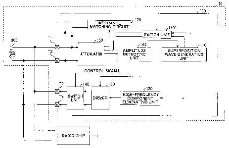
FIG. 3 is a diagram showing the amplifier
circuit 100 according to the embodiment.
As shown in FIG. 3, the amplifier circuit 100
includes the superposition wave generating unit 110, the
high-frequency component eliminating unit 120, the
driver 130, switch units 140 and 140', an attenuator 150,
an amplitude detecting unit 160, and an impedance
matching circuit 170. The amplifier circuit 100 further
includes a plurality of terminals T1-T4. In the
amplifier circuit 100, the terminals Ti and T2 serve as
input terminals, and the terminals T3 and T4 serve as
CA 02898428 2015-07-16
WO 2014/126026
PCT/JP2014/052986
-8-
output terminals.
In the amplifier circuit 100, the input
terminals Ti and T2 are connected to the antenna 200,
and the output terminals T3 and T4 are connected to the
radio chip 11. The antenna 200 is connected to the
radio chip 11.
The amplifier circuit 100 detects whether a
carrier signal received from the terminals Ti and T2 is
a predetermined carrier signal on which a predetermined
communication signal is carried, based on changes of the
amplitude value of the received carrier signal. When
the predetermined carrier signal is detected, the
amplifier circuit 100 superimposes the received carrier
signal with the superposition signal (superposition
wave) of the predetermined frequency, amplifies such
carrier signal, and outputs the amplified carrier signal
to the radio chip 11.
Next, the radio chip 11 used for the amplifier
circuit according to the embodiment will be described.
The radio chip 11 is a radio communication unit which
performs radio communication using the amplified carrier
signal from the amplifier circuit 100. For example, the
radio chip 11 may be an RFID chip, and the RFID chip 11
may include a memory which stores identification
information to identify a mobile device on which the
CA 02898428 2015-07-16
WO 2014/126026
PCT/JP2014/052986
-9-
radio chip 11 is mounted. Alternatively, the radio chip
11 may be an RFID controller which functions as an RFID
reader/writer.
For example, when the radio chip 11 as an RFID
chip approaches an RFID reader, the antenna module 10
connected to the radio chip 11 receives a carrier signal
of a predetermined frequency (e.g., 13.56 MHz) sent by
the RFID reader via the antenna 200.
In the antenna module 10 according to the
embodiment, when the carrier signal received by the
antenna 200 carries a communication signal representing
information by changes of the signal amplitude, the
amplifier circuit 100 amplifies the received carrier
signal and outputs the amplified carrier signal to the
radio chip 11. In the following, the carrier signal
carrying the communication signal will be called a
modulation carrier signal.
When a modulation carrier signal is received
from the amplifier circuit 100, the radio chip 11
returns a response signal via the antenna module 10 by a
load modulation which changes a load (not shown) in the
radio chip 11. A period for which the radio chip 11
returns the response signal is a period for which the
antenna 200 receives a carrier signal whose amplitude
value does not change.
CA 02898428 2015-07-16
WO 2014/126026
PCT/JP2014/052986
-10-
FIG. 4 is a diagram showing a modulation
carrier signal input to the amplifier circuit. In FIG.
4, an example of the modulation carrier signal sent by
the RFID reader is illustrated. As shown in FIG. 4, it
is assumed that the modulation carrier signal sent by
the RFID reader in this example is represented by a
carrier signal in which signal waves of amplitude H1 and
signal waves of amplitude H2 are alternately present at
a predetermined frequency.
In the amplifier circuit 100 according to the
embodiment, reception of a modulation carrier signal is
detected, the superposition wave is superimposed on the
modulation carrier signal, and the resulting modulation
carrier signal is amplified and output to the radio chip
11. The radio chip 11 operates in response to the
amplified modulation carrier signal received from the
amplifier circuit 100 as an energy source, converts the
identification information stored in the memory into the
amplitude of the non-modulation range of the amplified
modulation carrier signal, and returns the resulting
signal to an RFID reader.
The details of the amplifier circuit 100
according to the embodiment will be described. As
described above, the amplifier circuit 100 includes the
superposition wave generating unit 110, the high-
CA 02898428 2016-11-18
76311-51
-11-
frequency component eliminating unit 120, the driver 130,
the switch units 140 and 140', the attenuator 150, the
amplitude detecting unit 160, and the impedance matching
circuit 170.
The superposition wave generating unit 110
generates a superposition wave of a predetermined
frequency so that the superposition wave is superimposed
on the modulation carrier signal received from the
antenna 200. In this embodiment, the generated
superposition wave is synchronized in phase with the
modulation carrier signal which is received from, for
example, an RFID reader, and the frequency of the
superposition wave is equal to the frequency of the
modulation carrier signal. Alternatively, the phase of
the superposition wave may not be the same as the phase
of the modulation frequency. Note that the
superposition wave generating unit 110 in this
embodiment supplies a superposition signal of a
frequency equal to the frequency of the received carrier
signal to the attenuator 150 via the switch unit 140' at
the time of the impedance matching which will be
described later.
The high-frequency component eliminating unit
120 eliminates a high-frequency component from the
superposition wave generated by the superposition wave
CA 02898428 2015-07-16
WO 2014/126026
PCT/JP2014/052986
-12-
generating unit 110. The driver 130 outputs an
amplified carrier signal that is obtained by adding the
superposition wave to the modulation carrier signal and
amplifying the modulation carrier signal. In the
following, the carrier signal obtained by adding the
superposition wave to the modulation carrier signal and
amplifying the modulation carrier signal will be called
an amplified modulation carrier signal.
The switch unit 140 is provided to control
connection between the output of the driver 130 and the
output terminals T3 and T4. Turning ON and OFF of the
switch unit 140 is controlled in response to a control
signal output from the amplitude detecting unit 160.
The attenuator 150 attenuates the carrier
signal received from the terminals Ti and T2. The
resulting carrier signal at the output of the attenuator
150 is supplied to the impedance matching circuit 170.
The amplitude detecting unit 160 detects a
modulation carrier signal from the carrier signal
received from the terminals Ti and T2 via the attenuator
150, and supplies the detected modulation carrier signal
to the driver 130. When the modulation carrier signal
is detected, the amplitude detecting unit 160 outputs a
control signal to the switch unit 140 so that the switch
unit 140 is turned ON by the control signal. The
CA 02898428 2016-11-18
76311-51
-13-
details of the amplitude detecting unit 160 will be
described later.
The impedance matching circuit 170 is
connected between the terminals Ti, T2 and the
attenuator 150 and performs matching of the impedance of
the antenna module 10 as a whole. The impedance
matching circuit 170 controls turning ON and OFF of the
switch unit 140% The details of the impedance matching
circuit 170 will be described later.
Next, operation of the amplifier circuit 100
according to the embodiment relating to the
amplification of a carrier signal will be described.
First, operation of the antenna module 10 to
receive a modulation carrier signal will be described.
In the antenna module 10, when a carrier signal is
received from the antenna 200, the input carrier signal
is supplied to the amplitude detecting unit 160 via the
attenuator 150.
The amplitude detecting unit 160 detects
whether the received signal is a modulation carrier
signal based on the amplitude of the carrier signal
received via the attenuator 150. For example, the
amplitude detecting unit 160 may be implemented by a
binarizing circuit, such as a comparator including a
carrier eliminating filter. When the amplitude value of
CA 02898428 2015-07-16
WO 2014/126026
PCT/JP2014/052986
-14-
the carrier signal received from the attenuator 150
indicates the amplitude H1 (FIG. 4), the amplitude
detecting unit 160 may output a high-level (H level)
binary signal. When the amplitude value of the carrier
signal indicates the amplitude H2 (FIG. 4), the
amplitude detecting unit 160 may output a low-level (L
level) binary signal. In the following, the binary
signal output by the amplitude detecting unit 160 based
on the amplitude detected by the amplitude detecting
unit 160 will be called a modulation binary signal.
For example, when the binary value of the
modulation binary signal output by the amplitude
detecting unit 160 changes in a sequential pattern of 1
(the H level at a first period Ti), 0 (the L level at a
second period T2), 1 (the H level at a third period T3),
... as shown in FIG. 4, the amplitude detecting unit 160
detects the carrier signal input to the terminals Ti and
T2 as being the modulation carrier signal. However, the
method of detecting the modulation carrier signal by the
amplitude detecting unit 160 is not limited to the
above-described pattern method. For example, the
amplitude detecting unit 160 may be configured to detect
the input carrier signal as being the modulation carrier
signal when the binary value of the modulation binary
signal changes in another predetermined sequential
CA 02898428 2015-07-16
WO 2014/126026
PCT/JP2014/052986
-15-
pattern.
When the modulation carrier signal is detected,
the amplitude detecting unit 160 outputs a control
signal to the switch unit 140 so that the switch unit
140 is turned ON or OFF. Specifically, the amplitude
detecting unit 160 outputs the control signal causing
the switch unit 140 to be turned ON, when the modulation
carrier signal is detected. Further, the amplitude
detecting unit 160 outputs the detected modulation
carrier signal to the driver 130 at the same time.
In this embodiment, the input carrier signal
is supplied to the superposition wave generating unit
110 via the attenuator 150 and the driver 130. It is
preferred that the superposition wave generating unit
110 is able to perform phase correction to match the
phase of the carrier signal and the phase of the
superposition wave. For example, the superposition wave
generating unit 110 may be implemented by a PLL (phase
locked loop) circuit.
When the switch unit 140 is turned ON by the
control signal, the driver 130 is connected to the
terminals T3 and T4 by the ON-state switch unit 140.
In this embodiment, the superposition wave
generated by the superposition wave generating unit 110
and the modulation binary signal supplied through the
CA 02898428 2015-07-16
WO 2014/126026 PCT/JP2014/052986
-16-
amplitude detecting unit 160 are input to the driver 130.
In the driver 130, the modulation carrier signal is
converted into an amplified modulation carrier signal
which is obtained by adding the superposition wave to
the modulation carrier signal and amplifying the
modulation carrier signal. This amplified modulation
carrier signal is supplied to the radio chip 11 via the
terminals T3 and T4.
Next, operation of the antenna module 10 to
transmit a response signal output from the radio chip 11
will be described.
When a response signal output from the radio
chip 11 is transmitted to an RFID reader, the antenna
module 10 according to the embodiment does not performs
the amplification of the response signal. The signal
output from the radio chip 11 is a signal in which the
amplitude value of the amplified modulation carrier
signal is changed by the load modulation. In this case,
the amplitude detecting unit 160 detects that the
received signal is not the predetermined carrier signal.
In the antenna module 10, the terminals Ti and
T2 are connected also to the radio chip 11. Hence,
there is a case in which the response signal output from
the radio chip 11 may be input to the antenna module 10.
In this case, the amplitude value of the carrier signal
CA 02898428 2015-07-16
WO 2014/126026 PCT/JP2014/052986
-17-
input to the terminals Ti and T2 does not match the
predetermined pattern. Hence, the switch unit 140 is in
an OFF state, the driver 130 is not connected to the
terminals T3 and T4, and the antenna module 10 does not
output any signal. Therefore, in this case, the signal
output from the radio chip 11 is simply supplied to the
antenna 200.
Accordingly, in this embodiment, only when the
carrier signal received from the antenna 200 is the
modulation carrier signal carrying the communication
signal, the amplified modulation carrier signal obtained
by adding the superposition wave to the modulation
carrier signal is supplied to the radio chip 11.
Therefore, in the amplifier circuit according to the
embodiment, a small-sized antenna may be provided and
the communication performance may be maintained.
In the above embodiment, when the modulation
carrier signal is detected, the amplitude detecting unit
160 outputs the control signal to the switch unit 140 so
that the switch unit 140 is turned ON, and the driver
130 is connected to the terminals T3 and T4. However,
the present disclosure is not limited to this embodiment.
For example, the above embodiment may be
modified so that only when the amplitude value of the
carrier signal indicates the amplitude H1, the amplitude
CA 02898428 2015-07-16
WO 2014/126026 PCT/JP2014/052986
-18-
detecting unit 160 outputs the control signal to the
switch unit 140 so that the switch unit 140 is turned ON
to connect the driver 130 to the terminals T3 and T4.
In this case, the switch unit 140 is turned ON at the
first period Ti and at the third period T3 respectively
as shown in FIG. 4 and the superposition wave is added
to the carrier signal. Hence, the amplitude value of
the amplified modulation carrier signal output from the
driver 130 is increased only at the periods Ti and T3
respectively, and the amount of the amplitude change may
be increased.
In the above embodiment, the antenna module 10
has the composition including the amplifier circuit 100
and the antenna 200. Alternatively, the antenna module
10 may further include the radio chip 11 in addition to
the amplifier circuit 100 and the antenna 200. Further,
in the above embodiment, the radio chip 11 and the
amplifier circuit 100 are connected in parallel with the
antenna 200. The present disclosure is not limited to
this embodiment. For example, the radio chip 11 may be
connected to the latter-stage part of the amplifier
circuit 100.
Next, the impedance matching performed in the
amplifier circuit 100 according to the embodiment will
be described. In the amplifier circuit 100 according to
I
CA 02898428 2016-11-18
76311-51
-19-
the embodiment, matching of the impedance of the antenna
module 10 is performed. More specifically, the
amplifier circuit 100 performs matching of the impedance
of the antenna module 10 by using the impedance matching
circuit 170 so that the frequency of the carrier signal
is changed to a resonant frequency.
Next, the impedance matching circuit 170 will
be described with reference to FIG. 5. FIG. 5 is a
diagram showing the impedance matching circuit 170 in
the amplifier circuit 100 according to the embodiment.
As shown in FIG. 5, the impedance matching
circuit 170 includes a switch unit 140'and a matching
control unit 190. The switch unit 140'includes a
plurality of capacitors Cl-C connected in parallel and a
plurality of switches SW1-SWn respectively provided for
connecting the capacitors Cl-C to the terminals Ti and
T2. The switch unit 140'is connected to the matching
control unit 190. The matching control unit 190 selects
some of the capacitors included in the switch unit 140'
so that the selected capacitors may be connected to the
terminals Ti and T2.
In the switch unit 140, the switches SW1-SWn
correspond to the capacitors Cl-C respectively, and
turning ON and OFF of the switches SW1-SWn is controlled
by the matching control unit 190.
CA 02898428 2016-11-18
76311-51
-20-
The matching control unit 190 includes a
switch control unit 191, an impedance matching unit 192,
a combination extracting unit 193, an impedance setting
unit 194, and a memory unit 195.
The switch control unit 191 controls turning
ON and OFF of the switch unit 140'. The impedance
matching unit 192 changes the switches SW1-SWn which are
turned ON and changes the capacity of the switch unit
140'so that matching of the impedance of the antenna
module 10 is performed.
The combination extracting unit 193 extracts a
combination of capacitors from among all possible
combinations of the capacitors Cl-Cn included in the
switch unit 140'with which the amplitude (output value)
of the signal output by the attenuator 150 is at the
maximum.
Next, operation of the impedance matching
circuit 170 in the amplifier circuit 100 according to
the embodiment will be described. The impedance
matching which will be described later may be performed
upon startup of the device carrying the antenna module
10.
During the impedance matching, the impedance
matching circuit 170 causes the switch control unit 191
to turn ON the switch unit 140'so that the superposition
I
CA 02898428 2016-11-18
76311-51
-21-
wave generating unit 110 and the attenuator 150 are
connected together via the switch 140: Specifically,
the switch control unit 191 causes the switch unit 140 '
to be turned ON so that the superposition wave
generating unit 110 and the attenuator 150 are connected
together via the ON-state switch unit 140'.
When the superposition wave generating unit
110 and the attenuator 150 are connected, a
superposition signal of a frequency which is the same as
the frequency of the carrier signal, generated by the
superposition wave generating unit 110, is input to the
attenuator 150. For example, the frequency of the
signal generated at this time may be 13.56 MHz.
Subsequently, the impedance matching circuit
170 causes the impedance matching unit 192 to turn ON
the switches SW1-SWn included in the switch unit 140'
sequentially switch by switch.
The impedance matching unit 192 controls
turning ON and OFF of the switches SW1-SWn and acquires
= 20 respective output values of the attenuator 150
corresponding to all capacity values that may be taken
for all possible combinations of the capacitors Ci-Cn of
the switch unit 140% Subsequently, the combination
extracting unit 193 extracts a combination of capacitors
from among the capacitors Cl-Cn for which the acquired
CA 02898428 2016-11-18
76311-51
-22-
output value is at the maximum.
Subsequently, the impedance setting unit 194
sets up corresponding ones of the switches SW1-SWn in
the switch unit 140'for turning ON the extracted
capacitors to be in an ON state. For example, the
information indicating which of the switches SW1-SWn in
the switch unit 140'are set up in an ON state is stored
in the memory unit 195 as setting information.
Accordingly, in this embodiment, the output
value of the attenuator 150 for the combination of
capacitors corresponding to the ON-state switches
indicated by the setting information is at the maximum,
and the frequency of the carrier signal may be changed
to a resonant frequency. Therefore, the impedance of
the antenna module 10 according to the embodiment may be
changed to an optimal value.
In the above embodiment, the impedance when
the output value of the attenuator 150 is at the maximum
is used as the matched impedance. However, the present
disclosure is not limited to this embodiment. For
example, when there are very many combinations of
capacitors that must be monitored, impedance when the
output value of the attenuator 150 is greater than a
predetermined threshold value may be used as the matched
impedance.
CA 02898428 2015-07-16
WO 2014/126026
PCT/JP2014/052986
-23-
In this case, the combination extracting unit
193 compares the output value of the attenuator 150 with
the threshold value stored beforehand in the memory unit
195. When the output value of the attenuator 150 is
less than the threshold value, the impedance matching
unit 192 changes the ON-state switches of the switches
SW1-SWn.
For example, the impedance matching unit 192
turns ON the switch SW1 and connects the capacitor C1 to
the terminals Ti and T2. At this time, the combination
extracting unit 193 detects whether the output value of
the attenuator 150 is greater than the threshold value.
When it is detected that the output value of the
attenuator 150 is less than the threshold value, the
impedance matching unit 192 turns ON the switches SW1
and SW2, and the same detecting process is repeated.
When it is detected that the output value of
the attenuator 150 is greater than the threshold value,
the impedance setting unit 194 sets up the switches SW1
and SW2 for that combination of capacitors as being the
ON state switches.
In this embodiment, the threshold value is
predetermined as being a value adequate for performing
radio communication. Hence, in this embodiment, the
impedance matching may be performed so that the output
I
CA 02898428 2016-11-18
76311-51
-24-
value of the attenuator 150 is greater than the
threshold value, and the communication performance may
be maintained.
In this embodiment, the impedance matching
circuit 170 included in the amplifier circuit 100
performs the impedance matching, and it is unnecessary
to perform matching of the impedance for each of
individual devices on which the antenna module 10 is
carried.
In the above embodiment, the impedance
matching circuit 170 performs the impedance matching by
using the plural capacitors in the switch unit 140'which
are connected in parallel. However, the present
disclosure is not limited to this embodiment. For
example, a plurality of resistors connected in series
may be used for performing the impedance matching.
In this embodiment, the impedance matching for
every device may be automatically performed by matching
the impedance of the antenna module 10, and the
communication performance may be maintained.
Next, FIG. 6 is a diagram showing an amplifier
circuit 100A according to another embodiment.
In this embodiment, a superposition signal of
a predetermined frequency is superimposed on a carrier
signal received from an antenna, the superposition
CA 02898428 2015-07-16
WO 2014/126026 PCT/JP2014/052986
-25-
signal is synchronized in phase with the carrier signal,
and the carrier signal superimposed with the
superposition signal is output to a radio communication
device. Hence, a small-sized antenna may be provided
and the communication performance may be maintained.
As shown in FIG. 6, the amplifier circuit 100A
includes a superposition wave generating unit 110A, a
high-frequency component eliminating unit 120, a driver
130, a switch unit 140, a subtractor unit 145, an
attenuator 150, and an amplitude detecting unit 160.
The amplifier circuit 100A further includes a plurality
of terminals T1-T4. In the amplifier circuit 100A, the
terminals Ti and T2 serve as input terminals, and the
terminals T3 and T4 serve as output terminals.
In the amplifier circuit 100A, the input
terminals Ti and T2 are connected to the antenna 200,
and the output terminals T3 and T4 are connected to the
radio chip 11. The antenna 200 is connected to the
radio chip 11 via an impedance matching circuit 12. The
impedance matching circuit 12 is a circuit which
performs matching of the impedance between the antenna
200 and the radio chip 11.
The amplifier circuit 100A detects whether a
carrier signal received from the terminals Ti and T2 is
a predetermined carrier signal on which a predetermined
CA 02898428 2015-07-16
WO 2014/126026 PCT/JP2014/052986
-26-
communication signal is carried, based on changes of the
amplitude value of the received carrier signal. When
the predetermined carrier signal is detected, the
amplifier circuit 100A superimposes the received carrier
signal with a superposition signal (superposition wave)
of a predetermined frequency synchronized in phase with
the received carrier signal, amplifies such carrier
signal and outputs the amplified carrier signal to the
impedance matching circuit 12 and the radio chip 11.
The radio chip 11 used for the amplifier
circuit 100A according to this embodiment is essentially
the same as the radio chip 11 used for the amplifier
circuit 100 according to the previously described
embodiment, and a description thereof will be omitted.
In the amplifier circuit 100A shown in FIG. 6,
the superposition wave generating unit 110A generates a
superposition wave of a predetermined frequency so that
the superposition wave is superimposed on the modulation
carrier signal received from the antenna 200. In this
embodiment, the generated superposition wave is
synchronized in phase with the modulation carrier signal
which is received from, for example, an RFID reader, and
the frequency of the superposition wave is equal to the
frequency of the modulation carrier signal. For example,
the superposition wave generating unit 110A may be
CA 02898428 2015-07-16
WO 2014/126026
PCT/JP2014/052986
-27-
implemented by a PLL (phase locked loop) circuit.
The high-frequency component eliminating unit
120 eliminates a high-frequency component from the
superposition wave generated by the superposition wave
generating unit 110A. The driver 130 outputs an
amplified modulation carrier signal that is obtained by
adding the superposition wave to the modulation carrier
signal and amplifying the modulation carrier signal.
The switch unit 140 is provided to control
connection between the output of the driver 130 and the
output terminals T3 and T4. Turning ON and OFF of the
switch unit 140 is controlled in response to a control
signal output from the amplitude detecting unit 160.
The subtractor unit 145 is connected between
the input terminals Tl and T2 and the input of the
attenuator 150 and subtracts the signal from the output
of the driver 130 from the carrier signal from the input
terminals Ti and T2.
The attenuator 150 attenuates the amplitude of
the carrier signal from the output of the subtractor
unit 145. The amplitude detecting unit 160 detects a
modulation carrier signal from the carrier signal
received from the terminals Ti and T2 via the attenuator
150, and supplies the detected modulation carrier signal
to the driver 130. When the modulation carrier signal
CA 02898428 2015-07-16
WO 2014/126026
PCT/JP2014/052986
-28-
is detected, the amplitude detecting unit 160 outputs a
control signal to the switch unit 140 so that the switch
unit 140 is turned ON by the control signal.
Next, operation of the antenna module 10A
according to the embodiment will be described. First,
operation of the antenna module 10A to receive a
modulation carrier signal will be described. In the
antenna module 10A, when a signal is received from the
input terminals Ti and T2 via the antenna 200, the
received signal is supplied to the subtractor unit 145.
The subtractor unit 145 subtracts the signal from the
output of the driver 130 from the received signal and
outputs the resulting signal to the attenuator 150 as a
carrier signal. This carrier signal is supplied to the
amplitude detecting unit 160 via the attenuator 150.
The amplitude detecting unit 160 detects
whether the received signal is a modulation carrier
signal based on the amplitude of the carrier signal
received via the attenuator 150. For example, the
amplitude detecting unit 160 may be implemented by a
binarization circuit, such as a comparator including a
carrier eliminating filter. When the amplitude value of
the carrier signal received from the attenuator 150
indicates the amplitude H1 (FIG. 4), the amplitude
detecting unit 160 may output a high-level (H level)
CA 02898428 2015-07-16
WO 2014/126026
PCT/JP2014/052986
-29-
binary signal. When the amplitude value of the carrier
signal indicates the amplitude H2 (FIG. 4), the
amplitude detecting unit 160 may output a low-level (L
level) binary signal. In the following, the binary
signal output by the amplitude detecting unit 160 based
on the amplitude detected by the amplitude detecting
unit 160 will be called a modulation binary signal.
For example, when the binary value of the
modulation binary signal output by the amplitude
detecting circuit 160 changes in a sequential pattern of
1 (the H level at a first period Ti), 0 (the L level at
a second period T2), 1 (the H level at a third period
T3), ... as shown in FIG. 4, the amplitude detecting
circuit 160 detects the carrier signal input to the
terminals Ti and T2 as being the modulation carrier
signal. However, the method of detecting the modulation
carrier signal by the amplitude detecting unit 160 is
not limited to the above-described pattern method.
Alternatively, the amplitude detecting unit 160 may be
configured to detect the input carrier signal as being
the modulation carrier signal when the binary value of
the modulation binary signal changes in a predetermined
sequential pattern, for example.
When the modulation binary signal is detected,
the amplitude detecting unit 160 outputs a control
CA 02898428 2015-07-16
WO 2014/126026 PCT/JP2014/052986
-30-
signal to the switch unit 140 so that the switch unit
140 is turned ON or OFF. Specifically, the amplitude
detecting unit 160 outputs the control signal causing
the switch unit 140 to be turned ON, when the modulation
carrier signal is detected. Further, the amplitude
detecting unit 160 outputs the detected modulation
carrier signal to the driver 130 at the same time.
In this embodiment, the input carrier signal
is supplied to the superposition wave generating unit
110A via the attenuator 150. It is preferred that the
superposition wave generating unit 110A is able to
perform phase correction to match the phase of the
carrier signal and the phase of the superposition wave.
When the switch unit 140 is turned ON by the
control signal, the driver 130 is connected to the
terminals T3 and T4 by the ON-state switch unit 140.
In this embodiment, the superposition wave
generated by the superposition wave generating unit 110A
and the modulation carrier signal supplied through the
amplitude detecting unit 160 are input to the driver 130.
In the driver 130, the modulation carrier signal is
converted into an amplified modulation carrier signal
which is obtained by adding the superposition wave to
the modulation Carrier signal and amplifying the
modulation carrier signal. This amplified modulation
CA 02898428 2015-07-16
WO 2014/126026
PCT/JP2014/052986
-31-
carrier signal is supplied to the radio chip 11 via the
terminals T3 and T4.
Next, a function of the subtractor unit 145 in
the amplifier circuit 100A according to the embodiment
will be described. The subtractor unit 145 is a carrier
detecting unit adapted to detect a carrier signal from
the signal received from the terminals Ti and T2 with
good precision.
The terminals Ti and T2 of the amplifier
circuit 100A according to the embodiment are connected
to the terminals T3 and T4 via the impedance matching
circuit 12. In the amplifier circuit 100A, there may be
a case in which the signal output from the terminals T3
and T4 of the amplifier circuit 100A is added to the
carrier signal input from the terminals Ti and T2. In
such a case, the amplitude value of the carrier signal
may be altered due to the output signal of the amplifier
circuit 100A itself, and it may be difficult to
correctly detect the carrier signal as being a
modulation carrier signal.
To eliminate the problem, the subtractor unit
145 subtracts the signal from the output of the driver
130 from the signal received from the terminals Ti and
T2. Hence, as a result of the subtraction, the output
of the subtractor unit 145 provides only the carrier
CA 02898428 2015-07-16
WO 2014/126026 PCT/JP2014/052986
-32-
signal received from the antenna 200.
Accordingly, in this embodiment, the carrier
signal received from the antenna 200 may be detected
with good precision. Hence, the amplitude detecting
unit 160 may detect changes of the amplitude value of
the carrier signal correctly. Further, the
superposition wave generating unit 110A may generate the
superposition wave of the frequency which is equal to
the frequency of the carrier signal, the superposition
wave being synchronized in phase with the carrier signal.
Next, operation of the antenna module 10A
according to the embodiment to transmit a response
signal output from the radio chip 11 will be described.
In the antenna module 10A, the terminals Ti
and T2 of the amplifier circuit 100A are connected to
the radio chip 11. Hence, there may be a case in which
the response signal output from the radio chip 11 is
input to the antenna module 10A. In such a case, the
amplitude value of the carrier signal received from the
terminals Tl and T2 may be altered due to the input
signal to the amplifier circuit 100A. Hence, the switch
unit 140 remains in an OFF state, the driver 130 is not
connected to the terminals T3 and T4, and the antenna
module 10A does not output any signal.
Accordingly, only the signal output from the
CA 02898428 2015-07-16
WO 2014/126026 PCT/JP2014/052986
-33-
radio chip 11 is supplied to the antenna 200 and
transmitted from the antenna 200.
As described above, in this embodiment, only
when the carrier signal received from the antenna 200 is
detected as being the modulation carrier signal on which
the communication signal is carried, the amplified
modulation carrier signal which is obtained by adding
the superposition wave to the modulation carrier signal
and amplifying the modulation carrier signal may be
supplied to the radio chip 11. Therefore, in the
amplifier circuit 100A according to the embodiment, a
small-sized antenna may be provided and the
communication performance may be maintained.
In the above embodiment, when the modulation
carrier signal is detected, the amplitude detecting unit
160 outputs the control signal to the switch unit 140 so
that the switch unit 140 is turned ON, and the driver
130 is connected to the terminals T3 and T4. However,
the present disclosure is not limited to this embodiment.
For example, the above embodiment may be
modified so that only when the amplitude value of the
carrier signal indicates the amplitude H1, the amplitude
detecting unit 160 outputs the control signal to the
switch unit 140 so that the switch unit 140 is turned ON
to connect the driver 130 to the terminals T3 and T4.
CA 02898428 2015-07-16
WO 2014/126026
PCT/JP2014/052986
-34-
In this case, the switch unit 140 is turned ON at the
first period Ti and at the third period T3 respectively
as shown in FIG. 4 and the superposition wave is added
to the carrier signal. Hence, the amplitude value of
the amplified modulation carrier signal output from the
driver 130 is increased only at the periods Ti and T3
respectively, and the amount of the amplitude change may
be increased.
Furthermore, the above embodiment may be
modified so that a superposition wave having a phase
opposite to the phase of the carrier signal is generated
and the superposition wave having the opposite phase is
added to the carrier signal only when the amplitude
value of the carrier signal indicates the amplitude H2.
In this case, the amplitude value H2 of the carrier
signal is canceled by the superposition wave added
thereto, and the amplitude change of the modulation
carrier signal may be increased.
In the above embodiment, the antenna module
10A has the composition including the amplifier circuit
100A and the antenna 200. Alternatively, the antenna
module 10A may further include the radio chip 11 in
addition to the amplifier circuit 100A and the antenna
200. Further, in the above embodiment, the radio chip
11 and the amplifier circuit 100A are connected in
CA 02139138 23157-16
WO 2014/126026
PCT/JP2014/052986
-35-
parallel with the antenna 200. The present disclosure
is not limited to this embodiment. For example, the
radio chip 11 may be connected to the latter-stage part
of the amplifier circuit 100A.
Next, an amplifier circuit 100B according to
another embodiment will be described. The amplifier
circuit 1003 according to this embodiment differs from
the amplifier circuit 100A according to the previously
described embodiment in that an additional antenna which
functions as a carrier detecting unit is provided.
Other elements of the amplifier circuit 100B which are
essentially the same as corresponding elements of the
amplifier circuit 100A are designated by the same
reference numerals, and a description thereof will be
omitted.
FIG. 7 is a diagram showing the amplifier
circuit 100B according to this embodiment.
As shown in FIG. 7, an antenna module 10B
includes the amplifier circuit 1003 according to the
embodiment, an antenna 200, and an antenna 210. The
amplifier circuit 1003 includes a superposition wave
generating unit 110B, a high-frequency component
eliminating unit 120, a driver 130, a switch unit 140,
attenuators 150 and 155, and an amplitude detecting unit
160. The amplifier circuit 100B further includes a
CA 02898428 2015-07-16
WO 2014/126026
PCT/JP2014/052986
-36-
plurality of terminals T1-T6. In the amplifier circuit
100B, each of the antennas 200 and 210 is implemented by
an antenna with equivalent characteristics. Hence, each
of the antennas 200 and 210 receives a carrier signal in
the same manner.
In the amplifier circuit 100B, the antenna 210
is connected to the attenuator 155 via the terminals T5
and T6. An output signal from the output of the
attenuator 155 is supplied to the superposition wave
generating unit 110B.
When the amplitude detecting unit 160 detects
the carrier signal received from the antenna 200 as
being a modulation carrier signal, the superposition
wave generating unit 110B generates a superposition wave
of a predetermined frequency based on the carrier signal
received from the antenna 210. For example, the
superposition wave generating unit 110B is implemented
by a PLL circuit. Specifically, the superposition wave
generating unit 110B generates a superposition wave
whose frequency is equal to the frequency of the carrier
signal received from the antenna 210, and the generated
superposition wave is synchronized in phase with the
carrier signal received from the antenna 210.
In this embodiment, the antenna 210 which
receives the carrier signal that is the same as that
CA 02898428 2015-07-16
WO 2014/126026
PCT/JP2014/052986
-37-
received by the antenna 200 is connected to the
superposition wave generating unit 1103 via the
attenuator 155, and the superposition wave generating
unit 110B generates the superposition wave based on the
carrier signal from the antenna 210. Hence, even when
the output signal of the amplifier circuit 100B output
from the terminals T3 and T4 is added to the carrier
signal received from the terminals Ti and T2, the
superposition wave generating unit 110B may detect the
carrier signal received from the antenna 210 with good
precision and generate the superposition wave whose
phase is synchronized with the phase of the received
carrier signal.
In the above embodiment, the superposition
wave generating unit 110B generates the superposition
wave when the modulation carrier signal is detected by
the amplitude detecting unit 160. However, the present
disclosure is not limited to this embodiment. For
example, the above embodiment may be modified so that
the superposition wave generating unit 1103 always
generates a superposition wave and supplies the
superposition wave to the high-frequency component
eliminating unit 120, because the amplitude detecting
unit 160 is not connected to the superposition wave
generating unit 110B in the amplifier circuit 1003.
CA 02898428 2015-07-16
WO 2014/126026 PCT/JP2014/052986
-38-
In this case, it is necessary that the
amplitude detecting unit 160 outputs a modulation
carrier signal to the driver 130 when the modulation
carrier signal is detected, and outputs the control
signal to the switch unit 140 so that the switch unit
140 is turned ON. In this way, only when the modulation
carrier signal is detected, the superposition wave
generated by the superposition wave generating unit 1103
based on the carrier signal received from the antenna
210 is superimposed on the modulation carrier signal
output from the amplitude detecting unit 160, and the
modulation carrier signal superimposed with the
superposition wave is supplied to the radio chip 11.
In the above embodiment, the attenuator 155 is
connected between the antenna 210 and the superposition
wave generating unit 110B. However, the present
disclosure is not limited to this embodiment. For
example, the antenna 210 may be directly connected to
the superposition wave generating unit 1103 without
utilizing the attenuator 155.
In the amplifier circuit according to the
embodiment, a small-sized antenna may be provided and
the communication performance may be maintained.
The amplifier circuit according to the present
disclosure is not limited to the above-described
CA 02898428 2016-11-18
76311-51
-39-
embodiments, and variations and modifications may be
made without departing from the scope of the present
disclosure.