Note : Les descriptions sont présentées dans la langue officielle dans laquelle elles ont été soumises.
CA 2926715 2017-06-20
1
Electro-optical modulator devices
Description
This relates to an electro-optical modulator device.
Such electro-optical modulator devices comprise, for example, a high frequency
electrode arrangement used for supplying a voltage across the optical
waveguides
of the modulators for creating a phase shift of the optical waves propagating
in the
waveguides. For example, travelling wave electrodes are used for supplying a
voltage to the optical modulator waveguides as disclosed in the publication
"High-
Speed III-V Semiconductor Intensity Modulators", Robert G. Walker, IEEE
Journal
of Quantum Electronics Vol. 27, No. 3, March 1991. Driver units are used to
provide a voltage fed to the travelling wave electrodes, wherein the driver
units are
connected to the travelling wave electrodes via bonding wires. The inductance
of
the bonding wires, however, causes reflection of the high frequency electrical
signal supplied to the travelling wave electrodes that may deteriorate the
frequency response of the modulators.
According to one embodiment, there is provided an electro-optical modulator
device, comprising
at least one electro-optical modulator having a first and a second optical
waveguide and an electrode arrangement for applying a voltage across the
optical
waveguide,
- wherein the electrode arrangement comprises a plurality of first
waveguide
electrodes and a plurality of second waveguide electrodes arranged on top of
the
first and the second optical waveguide, respectively,
wherein the first and second waveguide electrodes are capacitively coupled
to one another; and
CA 2926715 2017-06-20
2
- at least one driver unit for supplying a voltage to the electrode
arrangement;
and
- an electrical connection between the driver unit and the electrode
arrangement;
- wherein the electrode arrangement comprises a first electrical line
connected to the first waveguide electrodes and a second electrical line
connected
to the second waveguide electrodes, the first and the second electrical line
forming
a coplanar strip line,
wherein
the electrical connection between the driver unit and the electrode
arrangement
comprises a flexible coplanar strip line,
wherein the flexible coplanar strip line comprises at least two electrical
lines,
wherein a first one of the electrical lines of the flexible coplanar strip
line is
connected to the first electrical line of the electrode arrangement and a
second
one of the electrical lines of the flexible coplanar strip line is connected
to the
second electrical line of the electrode arrangement, and
wherein the driver unit is configured for supplying a differential voltage
signal to
the coplanar strip line formed by the first and the second electrical line of
the
electrode arrangement via the first and the second electrical line of the
flexible
coplanar strip line,
wherein
the flexible coplanar strip line is a part of a flexible contact structure
that in addition
to the electrical lines of the flexible coplanar strip line comprises a
plurality of
conducting lines connected to input contacts of an integrated circuit that
forms the
driver unit and configured for connecting external devices to the input
contacts.
According to another embodiment, there is provided an electro-optical
modulator
device, comprising
= CA 2926715 2017-06-20
2a
at least one electro-optical phase modulator having at least one active
optical waveguide and an electrode arrangement for applying a voltage across
the
active optical waveguide,
wherein the electrode arrangement comprises a plurality of waveguide
electrodes arranged on top of capacitive segments formed by the optical
waveguide;
at least one optically inactive capacitive element;
at least one driver unit for supplying a voltage to the electrode arrangement;
an electrical connection between the at least one driver unit driver unit and
the electrode arrangement, wherein the waveguide electrodes are capacitively
coupled to the at least one driver unit via the capacitive segments and the at
least
one capacitive element and the electrical connection,
wherein
the electrical connection between the at least one driver unit and the
electrode
arrangement comprises a flexible coplanar strip line.
CA 02926715 2016-04-06
WO 2015/075258 PCT/EP2014/075526
3
It is noted that the electrical connection (i.e. an electrical link) between
the driver unit and the
electrode arrangement may at least essentially consist of the flexible
coplanar strip line, wherein
the driver unit is directly connected to the electrode arrangement via the
flexible coplanar strip
line. However, it is also conceivable that the flexible coplanar strip line
only forms a segment of
the electrical connection between the driver unit and the electrode
arrangement such that the
connection comprises at least one other section that is not formed by a
flexible coplanar strip line.
The flexible coplanar strip line in particular permits to be adapted
(impedance matched) to the
coplanar strip line of the electrode arrangement of the modulator, wherein the
flexible coplanar
strip line and the coplanar strip line of the modulator may form a homogeneous
and impedance
matched line having improved high frequency characteristics. In particular,
the at least two
electrical lines of the flexible coplanar strip line are arranged on at least
one flexible layer, wherein
the two lines are arranged in a distance from one another that permits the
lines to act as an
electrical waveguide for conveying a high frequency mode from the driver unit
to the modulator.
For example, the distance between the first and the second electrical line of
the flexible coplanar
strip line is less than 25 pm, less than 10 pm or less than 5 pm (e.g. 2, 3 or
4 pm). The flexible
coplanar strip line may comprise exactly two electrical lines, wherein in
particular none of the two
electrical lines is grounded.
For example, modulator devices (i.e. the combination of the driver unit and
the modulator),
employed e.g. for long-distance applications, having power losses smaller than
400 mW may be
realized. Further, because of the possible low power consumption and the
possible compact
design of the modulator, compact high frequency modulator modules (having e.g.
a transmission
rate of at least 100 Gbit/s) can be fabricated (e.g. in the CFP4 module size).
Further, the thermal
conductivity of the flexible coplanar strip line may be lower than those of
conventional bonding
wires. Thus, thermal crosstalk between the driver unit and the modulator may
be lower. Further,
the distance between the driver unit (e.g. in the form of an integrated
circuit) and modulator may
be larger, thereby facilitating the assembly of the modulator device. For
example, the modulator
can be disposed on a thermoelectric cooler while the driver unit is arranged
on a housing part of
the modulator device.
CA 2926715 2017-06-20
=
4
The electrical lines of the flexible coplanar strip line may be bonded, e.g.
soldered
or glued (using a conductive adhesive) or by means of a metal connection, to
the
electrical lines of the modulator's electrode arrangement.
The flexible coplanar strip line further may be formed employing thin film
technology (that in particular permits the electrical lines of the flexible
coplanar
strip line to be produced with high precision). For example, the flexible
coplanar
strip line comprises two electrical lines arranged on at least one isolating
layer,
wherein the isolating layer may be formed from a polymer material such as
polyimide, a liquid crystal polymer - LCP or Benzocyclobutene - BCB, wherein
multiple polymer layers may be used. Examples of the principle fabrication of
isolating layers for a flexible electrical line are described in the article
"Multilayer
polyimide film substrates for interconnections in microsystems", A. Fach, Y.
Athanassov, U. Brunner, D. Hablutzel, B. Ketterer, J. Link,
MicrosystemTechnologies 5 (1999) 166- 168.
For example, the at least one isolating layer may have a thickness of less
than 50
pm, less than 25 pm or less than 15 pm. Further, the electrical lines of the
flexible
coplanar strip line may be fabricated using a lithographic process, wherein
the
electrical lines may be disposed on the flexible substrate by metal deposition
(using e.g. electroplating, vapor deposition or sputtering). It is noted,
however, that
instead of thin polyimide layers the flexible coplanar line may comprise a
(e.g.
single) isolating (e.g. foil-like) thicker substrate.
In particular, other components of the modulator device may be connected by
other flexible electrical lines (e.g. fabricated together with the flexible
coplanar strip
line). In particular, the driver unit (e.g. a driver IC) can be arranged on a
flexible
substrate together with the electrical lines of the flexible coplanar line and
other
wiring (e.g. using the flip-chip technology).Thus, a testable driver unit
having
= CA 2926715 2017-06-20
integrated connections to and from the driver unit can be generated, the
driver unit
being easily and cost-efficiently integrable into a module.
For example, the coplanar strip line formed by the first and the second
electrical
5 line is operated as a travelling wave electrode, e.g. of a Mach-Zehnder
modulator.
Further, the first and the second electrical line is capacitively coupled to
one
another via the capacitively coupled first and second waveguide electrodes.
For
example the optical waveguides of the modulator each comprise a plurality of
capacitive segments spaced apart from one another, the capacitive segments
each forming an electrical capacitor. The first and second waveguide
electrodes
are arranged on top of the capacitive segments such that they are capacitively
coupled to one another via the capacitive segments.
An example of a possible principal optical and electrical layout of such a
travelling
wave Mach-Zehnder modulator is described in the publication "45 GHz Bandwidth
Travelling Wave Electrode Mach-Zehnder Modulator with Integrated Spot Size
Converter", D. Hoffmann, Proceedings International Conference on Indium
Phosphide and Related Materials, p. 585, 2004. It is noted, however, that the
invention is of course not restricted to a particular electrode design but
could be
also used in other electrical circuits or to form other electrical circuits.
Further, the
another possible design is described in international patent application WO
2012/175551. For example, the modulator device comprises IQ modulators and/or
OFDM modulator(s) (e.g. in the form of a PIC - photonic IC).
The first and a second electrical line is driven symmetrically ("differential
drive"),
i.e. the driver unit is configured for supplying a differential voltage signal
to the
flexible coplanar strip and thus to the coplanar strip line of the modulator.
For
example, none of the electrical lines of the electrode arrangement and/or of
the
flexible coplanar strip line is grounded, wherein the driver unit is
configured for
supplying a first varying signal to the first electrical line of the electrode
' CA 2926715 2017-06-20
=
6
arrangement via the first electrical line of the flexible coplanar strip line
and a
second varying signal to the second electrical line of the electrode
arrangement
via the second electrical line of the flexible coplanar strip line.
Further, the first and the second electrical line may be formed at least
partially as
geometrically symmetric structures. For example, the first and the second
electrical line of the flexible coplanar strip line are formed as longitudinal
structures
which at least essentially extend parallel to one another.
The impedance of the driver unit at each one of its two output ports may be
essentially half of the impedance of the electrode arrangement. Moreover, the
driver unit may be configured in such a way that the first and the second
varying
signal supplied to the first and second electrical line, respectively, have
opposite
polarity (wherein the absolute voltage value of the first and the second
varying
signal may be at least essentially identical).
Examples of symmetrically driven electrodes are disclosed in the European
patent
applications EP 2 615 489 and EP 2 615 490.
Further, the first and the second electrical line of the flexible coplanar
strip line are
e.g. arranged on a (e.g. flexible) isolating layer at least partially adjacent
to one
another in a direction perpendicular to their longitudinal extension. However,
the
first and the second electrical line of the flexible coplanar strip line may
also be
= CA 2926715 2017-06-20
6a
arranged at least partially one above the other in a direction perpendicular
to the at
least one isolating layer.
The first and/or the second line of the flexible coplanar strip line may be
arranged
on a first isolating layer (e.g. a first polyimide layer) and may be covered
by a
second isolating layer (e.g. a second polyimide layer). For example, a second
isolating layer extends between a first portion and a second portion of the
second
electrical line. Moreover, two further lines may be arranged on the isolating
layer,
the further lines being grounded.
According to another embodiment, the driver unit is operated in open collector
mode or in open collector mode with back termination. Similarly, the driver
unit
may be operated in open drain or in open drain mode with back termination (if
the
driver unit is a CMOS device).
More particularly, the driver unit (e.g. a driver chip), the flexible coplanar
line, the
first and the second electrical line, a terminating resistors and a (blocking)
capacitive structure for galvanically separating the terminating resistors
(and e.g.
also the employed assembly and joining technology) can be regarded as integral
components of the open collector circuitry (e.g. a high frequency open
collector
circuitry) as will be explained in more detail below. In particular, an
immersive
electrical design of the driver unit, flexible coplanar line, the electrical
lines and a
terminating network (comprising at least one terminating resistors as set
forth
below) of the modulator will be carried out in particular to adapt the overall
impedance of these components and thus to optimize the
CA 02926715 2016-04-06
WO 2015/075258 PCT/EP2014/075526
7
performance of the modulator. It is noted that it is of course not necessary
to use open collector
circuitry. Rather, the driver unit may have an internal terminating resistance
that equals the
impedance of the electrode arrangement, wherein the impedance of the flexible
coplanar line, the
first and the second electrical line and other electrical components (such as
the terminating
resistor mentioned above) is matched to the internal terminating resistance of
the driver unit.
As set forth above, the modulator may comprises at least one terminating
resistor for terminating
the coplanar strip line formed by the first and the second electrical line,
wherein the terminating
resistor may be (physically) arranged between the first and the second
electrical line of the
electrode arrangement. For example, the terminating resistor is a single
resistor (having a
resistance of e.g. 50 Ohm), wherein the terminating resistor may be formed by
a material layer
(e.g. a thin film layer or a thin film layer packet). The terminating resistor
may be monolithically
integrated with the first and the second electrical line, i.e. it may be
arranged on the same
substrate as the first and the second electrical line. In that case only the
driver unit will be
connected to the first and the second electrical line of the modulator's
electrode arrangement via
a flexible coplanar strip line. However, the terminating resistor may also be
formed as a separate
component arranged e.g. on a different substrate (e.g. a ceramic substrate)
than the electrical
lines of the modulator and/or coupled to the first and the second electrical
line of the modulator
via a flexible coplanar strip line or e.g. via short bonding wires.
The modulator may also comprise two terminating resistors, wherein the two
terminating resistors
are connected to one another via an end contact. In particular, a first end of
the first one of the
terminating resistors is connected to the first electrical line and a second
end is connected to the
end contact. Similarly, a first end of the second terminating resistor is
connected to the second
electrical line and a second end is connected to the end contact. The two
terminating resistors
may be formed by material layers connected to one another by an end contact
layer forming the
end contact. It is also possible that the two terminating resistors are
galvanically separated by
connecting the terminating resistor to one another via a capacitor. Moreover,
at least one
capacitive structure may be provided that galvanically separates the two
terminating resistors.
For example, the capacitive structure comprises at least two electrically
conductive layers
arranged between the first and the second electrical line, wherein the at
least two layers are
separated by at least one dielectric layer.
. CA 2926715 2017-06-20
-
8
The flexible coplanar strip line may further be part of a flexible contact
structure
that comprises a plurality of conducting lines for connecting external devices
to
input contacts of the driver unit.
According to another aspect, an electro-optical modulator device is provided,
comprising
- at least one electro-optical modulator having a first and a second
optical
waveguide and an electrode arrangement for applying a voltage across the
optical
waveguide,
- wherein the electrode arrangement comprises a plurality of first
waveguide
electrodes and a plurality of second waveguide electrodes arranged on top of
the
first and the second optical waveguide, respectively,
- wherein the first and second waveguide electrodes are capacitively
coupled to
one another; and
- an electrical connection between the driver unit and the electrode
arrangement;
and
- a plurality of driver units, wherein each one of the driver units is
connected to one
of the first waveguide electrodes and to one of the second waveguide
electrodes
via an electrical connection that comprises a flexible coplanar strip line.
Thus, the waveguide electrodes can be driven individually (independent from
one
another) as described in the publication "10 Gb/s - 80-km operation of full C-
band
InP MZ modulator with linear-accelerator-type tiny in-line centipede electrode
structure directly driven by logic IC of 90-nm CMOS process", T. Kato et al.,
Optical Fiber Communication Conference and Exposition, 2011, p. 1.
According to yet another aspect, there is provided an electro-optical
modulator
device, comprising
' = CA 2926715 2017-06-20
8a
- at least one electro-optical phase modulator having at least one active
optical
waveguide and an electrode arrangement for applying a voltage across the
active
optical waveguide,
- wherein the electrode arrangement comprises a plurality of waveguide
electrodes
arranged on top of capacitive segments formed by the optical waveguide;
- at least one optically inactive capacitive element;
CA 02926715 2016-04-06
WO 2015/075258 PCT/EP2014/075526
9
- at least one driver unit for supplying a voltage to the electrode
arrangement;
- an electrical connection between the driver unit and the electrode
arrangement, wherein the
waveguide electrodes are capacitively coupled to the at least one driver unit
via the capacitive
segments and the capacitive element and the electrical connection, wherein
- the electrical connection between the at least one driver unit and the
electrode arrangement
comprises a flexible coplanar strip line.
A plurality of capacitive elements may be provided in the form of capacitive
segments formed by
a second waveguide that is optically inactive. On top of the second waveguide
(second)
waveguide electrodes may be provided such that the phase modulator is designed
similarly to the
travelling wave Mach-Zehnder modulator mentioned above, wherein, however, only
one of the
two optical waveguides is optically active and used for modulating the phase
of an optical signal.
In contrast to the Mach-Zehnder-modulator, however, the second, inactive
waveguide and thus
the second waveguide electrodes of the phase modulator may be broader than the
active optical
waveguide and the (first) waveguide electrodes on top of the optically active
waveguide.
According to an alternative embodiment, the phase modulator device comprises a
plurality of
driver units, which permit the waveguide electrodes to be driven individually
as described above.
However, it is noted the capacitive elements of the phase modulator device do
not necessarily
have to be formed by an (inactive) waveguide. Rather, in principle, any kind
of capacitive structure
may used that, in particular, is connected in series with the capacitive
segments formed by the
active optical waveguide.
According to yet another aspect, the invention relates to an electro-optical
modulator device, in
particular as described above, comprising
- at least one electro-optical modulator having at least one optical
waveguide and an electrode
arrangement for applying a voltage across the optical waveguide,
- wherein the electrode arrangement comprises a first and a second
electrical line forming a
coplanar strip line; and
- at least one terminating resistor terminating the first and a second
electrical line; and
CA 02926715 2016-04-06
WO 2015/075258 PCT/EP2014/075526
- an electrical connection between the terminating resistor and first and a
second electrical line,
wherein
- the electrical connection between the terminating resistor and the first
and the second electrical
line comprises a flexible coplanar strip line.
5
The first and the second electrical line in particular may be capacitively
coupled to one another.
For example, the electro-optical modulator is a Mach-Zehnder modulator or a
phase modulator
as described above.
Embodiments of the invention are explained in more detail hereinafter with
reference to the
10 Drawings, in which:
Figure 1A shows a perspective view of an electro-optical modulator
device according
to an embodiment of the invention;
Figure 1B relates to an alternative realization of the embodiment shown
in Fig. 1A;
Figure 1C relates to yet another alternative realization of the
embodiment shown in
Fig. 1A;
Figures 2A ¨ 2D illustrated different configurations of a flexible coplanar
strip line;
Figure 3 shows a diagram of a first open collector circuit for
operating an electro-
optic modulator device according to the invention;
Figure 4 shows a diagram of a second open collector circuit for
operating an
electro-optic modulator device according to the invention;
Figure 5 shows a diagram of a third open collector circuit for
operating an electro-
optic modulator device according to the invention;
Figure 6 depicts a variant of a terminating arrangement for
terminating the
electrode arrangement of a modulator;
CA 02926715 2016-04-06
WO 2015/075258 PCT/EP2014/075526
11
Figure 7 depicts another variant of a terminating arrangement for
terminating the
electrode arrangement of a modulator;
Figure 8A shows a top view of a detail of an electro-optical
modulator of a modulator
device according to yet another embodiment of the invention;
Figure 8B shows a sectional view of the modulator shown in Fig. 8A
along A-A;
Figure 8C shows a sectional view of the modulator shown in Fig. 8A
through its
capacitive structure (along line B-B in Fig. 8A);
Figure 9 shows a sectional view of another embodiment of the
capacitive structure;
Figure 10 illustrates the modulator device of Fig. 1 without the
driver unit;
Figure 11 shows a perspective view of a modulator device according to a
further
embodiment of the invention;
Figure 12 illustrates a perspective view of a modulator device
according to yet
another embodiment of the invention;
Figure 13 depicts a schennatical view of a multiple driver unit
embodiment of
modulator device according to an embodiment of the invention; and
Figure 14 shows a perspective view of an alternative realization of
the modulator
device of Fig. 13.
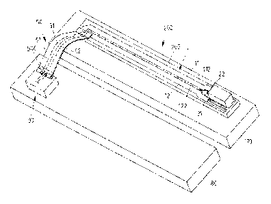
The electro-optical modulator device 200 according to the invention shown in
Figure 1A comprises
an open-collector capable Mach-Zehnder-modulator 100. The modulator 100
comprises an
electrode arrangement 1 having a first and a second electrical line 11, 12
forming a coplanar strip
line. The electrical lines 11,12 are connected to waveguide electrodes 113,
123 (see Fig. 8B) via
air bridges for applying a voltage across optical waveguides 112, 122 of the
modulator as in
principle known from the prior art. The modulator 100 (including a
semiconductor substrate 205
CA 02926715 2016-04-06
WO 2015/075258 PCT/EP2014/075526
12
on which the electrode arrangement 1 is arranged) is disposed on a first
substrate 70 (e.g. a
ceramic substrate). The optical and electrical layout of modulator 100 may
designed as described
in the above-mentioned publication "45 GHz Bandwidth Travelling Wave Electrode
Mach-Zehnder
Modulator with Integrated Spot Size Converter", D. Hoffmann, Proceedings
International
Conference on Indium Phosphide and Related Materials, p. 585, 2004.
Besides the modulator 100 the electro-optical modulator device 200 further
comprises a driver
unit 30 configured to supply a (high frequency) differential voltage to the
electrode arrangement
1 of modulator 100. The driver unit 30 is disposed on a second substrate 80
(e.g. a PCB) different
from the first substrate 70 and arranged in a distance from the first
substrate 70 such that a gap
(of e.g. of at least 200 pm) is present between the two substrates 70, 80.
Further, the driver unit 30 (i.e. an output port of the driver unit 30
comprising two output contacts
506) is electrically connected to the first and the second electrical line 11,
12 via an electrical
connection a flexible coplanar line 50. The flexible coplanar line 50
comprises electrical lines 51,
52 arranged at at least one flexible, foil-like substrate 61 (e.g. formed from
a polymer such as
polyinnide), wherein a first end of the electrical lines 51, 52 is connected
to the output contacts
506 and a second, opposite end is connected to the electrical lines 11, 12 of
the modulator's
electrode arrangement 1. Examples of the configuration of the flexible
coplanar line 50 are
described with reference to Fig. 2A ¨ 2D.
Figure 1B relates to an alternative realization of the modulator device
according to the invention.
The driver unit 30 in contrast to Fig. 1A is arranged on the second substrate
80 in flip chip
configuration, i.e. its contacts (such as the output contacts 506) face
downwards towards the
substrate 80. The output contacts 506 are connected to an electrical coplanar
strip line 90
arranged on the substrate 80, wherein one end of the flexible coplanar line 50
is connected to the
electrical line 90 and an opposite end connects to the electrical lines 11, 12
of the modulator. In
other words, the electrical connection between the driver unit 30 and the
electrode arrangement
1 does not only comprise the flexible coplanar line 50 but also the electrical
line 90, wherein a
high frequency electrical mode may be continuously guided via the connecting
coplanar strip lines
90 and 50 and the coplanar strip line formed by the electrical lines 11, 12 of
the modulator 100.
CA 02926715 2016-04-06
WO 2015/075258 PCT/EP2014/075526
13
It is noted that further electrical components (not shown) might be arranged
on the second
substrate 80 connected to the driver unit 30 via additional electrical lines
(not shown) arranged
on the substrate 80. According to another embodiment of the invention, the
modulator 100 may
be operated as a phase modulator, wherein only one of the optical waveguides
112, 122 is used
to modulate the phase of an optical signal. For example, the one of the
optical waveguides 112,
122 that is not used may be optically inactive, wherein, however, the
capacitive segments 114
and 124 (see Fig. 8B), respectively, formed by the optically inactive
waveguide are used as
capacitive elements. Thus, the waveguide electrodes of the optically active
waveguide are still
capacitively coupled to the driver unit via the capacitive segments of the two
waveguides.
According to the embodiment shown in Fig. 1C, the modulator 100 and the driver
unit 30 are
arranged on a common substrate 75.
The distance between the two (parallel) electrical lines 51, 52 is chosen to
be small enough that
the electrical lines 51, 52 from an electrical waveguide for conveying a high
frequency electrical
wave. For example, the distance between the electrical lines 51, 52 is smaller
than 25 pm
First endings of the electrical lines 51, 52 of the flexible coplanar line 50
are connected to an
output port of the driver unit, whereas second endings of the electrical lines
51, 52 are connected
to endings of the first and second electrical line 11, 12 of the modulator
100. Since the flexible
coplanar strip 50 provides an electrical waveguide, its impedance can be
better matched with the
impedance of the driver unit 30 and the electrode arrangement 1 of the
modulator such that the
high frequency performance of the modulator can be improved. Due to its
waveguide properties,
in turn, the flexible coplanar strip 50 in contrast to bonding wires does not
have to be very short
such that a good thermal separation between the driver unit 30 (that may warm
up during
operation) and the modulator 100 can be realized. For example, the driver unit
30 is arranged in
a distance of at least 1 mm from the modulator 100.
In order to terminate the coplanar strip line formed by the electrical lines
11, 12 of the modulator
100, two terminating resistors 21, 22 (each one having a resistance of e.g.
250) are arranged
between the electrical lines 11, 12, wherein the terminating resistors 21, 22
are formed as material
layers (e.g. Ni-Cr layers) arranged on a substrate together with the coplanar
strip line, i.e. the
terminating resistors 21, 22 are monolithically integrated with other
components of the electro-
CA 02926715 2016-04-06
WO 2015/075258 PCT/EP2014/075526
14
optic modulator. However, the terminating resistors 21, 22 may also be
fabricated separately (e.g.
on a different substrate) and connected to the electrical lines 11, 12 via
another flexible coplanar
strip line as shown in Fig. 11. Alternatively the terminating resistors 21, 22
may be conventionally
bonded (e.g. via short bonding wires) to the electrical lines 11, 12. Examples
of how the electrical
lines 11, 12 may be terminated are shown in Fig. 6 to 9.
Figures 2A ¨ 2D relate to embodiments of the flexible coplanar strip line 50.
According to Figure
2A, the electrical lines 51, 52 of the flexible coplanar strip line 50 are
arranged on the same side
of a first (e.g. flexible) electrically isolating layer 61 (e.g. a first
polyimide layer) next to one another
in the direction perpendicular to the longitudinal extension of the electrical
lines 51, 52. A second
isolating layer (e.g. a second polyimide layer) covers the first and the
second electrical line 51, 52
such that they are embedded by the isolating layers 61, 62. For example, the
thickness of each
one of the isolating layers 61, 62 is less than 20 pnn or less than 15 pm,
e.g. about 10 urn, wherein
the thickness of each one of the electrical lines 51, 52 (formed e.g. from a
metal such as gold) is
less than 10 pm or less than 8 pm (e.g. about 5 pm).
The flexible coplanar line 50 shown in Fig. 2A (and similar the flexible
coplanar lines illustrated in
Fig. 2B-D) can be fabricated using thin film technology, wherein for example
for fabricating the
first isolating layer 61 a polymer material is applied to a carrier substrate,
the electrical lines 51,
52 are deposited on the first isolating layer 61 and subsequently the second
isolating layer 62 is
applied. Finally, the carrier substrate is removed. It is noted that the
isolating layers 61, 62 are
not connected to one another by means of an adhesive, particularly to avoid
that gases are set
free from the adhesive. In particular, the isolating layers 61, 62 are formed
from a standard
isolating polymer used in solid state processes (such as liquid polyimides
fabricated by e.g. the
company "HD MicroSystems").
Figure 2B is related to another variant, wherein the electrical lines 51, 52
are arranged one above
the other in a direction perpendicular to the first isolating layer 61.
Further, a second isolating
layer 62 is arranged between the first and the second electrical line 51, 52
and a third isolating
layer 63 covers the upper second electrical line 52 such that the electrical
lines 51, 52 are
embedded by the isolating layers 61 ¨ 63.
CA 02926715 2016-04-06
WO 2015/075258 PCT/EP2014/075526
According to Fig. 2C, again three isolating layers 61-63 are provided, wherein
the first electrical
line 51 and a first portion 521 of the second electrical line 52 are disposed
on the first (lower)
isolating layer 61. The second (middle) isolating layer 62 is arranged on the
first electrical line 51
and the first portion 521 of the second electrical line 52, wherein a second
portion 523 of the
5 second electrical line 52 is arranged on top of the middle isolating
layer 62. The first portion 521
and the second portion 523 are (e.g. integrally) connected to one another by a
connecting portion
522 reaching trough a recess of the middle layer 62. The second portion 523 of
the second
electrical line 52 is covered by a third (upper) isolating layer 63.
10 The structure shown in Fig. 20 might be fabricated by arranging the
middle layer 62 on the first
electrical line 51 and the first portion 521 of the second electrical line 52.
Subsequently, an
opening is formed in the middle layer 62 and the connecting portion 522 is
generated by
depositing a metal (e.g. gold) in the region of the opening. Finally, the
second portion 523 is
generated to connect to the connecting portion 522.
According to the variant depicted in Fig. 2D, the flexible coplanar line 50 in
addition to the electrical
lines 51, 52 comprises two further electrical lines 53, 54, the further
electrical lines 53, 54 being
grounded (to realize a "ground-signal-signal-ground" configuration). The
further lines 53, 54 may
be arranged on the same side of the first isolating layer 61 as the first and
the second electrical
line 51, 52. Further, a second isolating layer 62 is arranged to cover the
first and the second
electrical line 51, 52 and the further electrical lines 53, 54.
Figure 3 illustrates a first example of an open collector circuit that may be
used to drive the
electrode arrangement 1 of modulator 100. The driver unit 30 supplies a
differential voltage to the
modulator's electrode arrangement 1 via the flexible coplanar strip line 50.
Two terminating
resistors 21, 22 are provided for terminating the coplanar strip line of the
modulator 100, wherein
the terminating resistors 21, 22 are connected to one another via an end
contact 23. The end
contact further connects to a supply voltage Vcc fed towards the collectors
401, 402 of two
transistors 41, 42 of the driver unit 30.
A modification of the open collector circuit shows Fig. 4, wherein the
terminating resistors 21, 22
are capacitively coupled to one another via a capacitor 31. A possible
realization of the capacitor
31 is depicted in Fig. 8A ¨ 8C. Further, two inductances 301, 302 are
connected to the terminating
CA 02926715 2016-04-06
WO 2015/075258 PCT/EP2014/075526
16
resistors 21, 22 via which the supply voltage Vcc is fed towards the
collectors 401, 402 of the
transistors 41, 42 of the driver unit 30. Supplying Vcc via the inductances
301, 302 has the
advantage that the supply power is guided around the terminating resistors 21,
22 such that a
power loss in the terminating resistors 21, 22 is avoided. It is noted that
the driver unit 30 may
also be a CMOS device, wherein an open drain circuit may be realized (by
supplying the voltage
Vcc to a drain of the driver unit's transistors). According to another
embodiment, the inductances
301, 302 are arranged between the driver unit 30 and the modulator 100.
Fig. 5 relates to another open collector circuitry that may be used to operate
the modulator 100,
wherein the driver unit 30 again is connected to the electrical lines 11, 12
of the modulator's
electrode arrangement via the flexible coplanar strip line 50. Furthermore,
the termination of the
modulator's coplanar strip line is realized by two terminating resistors 21,
22, each one of the
terminating resistors 21,22 being connected to ground via a capacitor 31a,
31b. An example of
how the two capacitors 31a, 31b may be realized is illustrated in Fig. 9.
Figure 6 illustrates a possible realization of a terminating network used for
the termination of the
electrical lines 11, 12 of the electrode arrangement 1 of the modulator 100.
The terminating
network comprises two terminating resistors 21, 22 (each one having a
resistance of e.g. 25 0)
arranged between the electrical lines 11, 12, wherein the terminating
resistors 21, 22 are formed
as material layers arranged on a substrate together with the coplanar strip
line, i.e. the terminating
resistors 21, 22 are monolithically integrated with other components of the
electro-optic
modulator. However, as mentioned above it is of course also possible that the
terminating
resistors 21, 22 are not monolithically integrated with the modulator. For
example, the resistors
21, 22 are arranged on a different substrate and are bonded to the electrical
lines 11, 12 of the
modulator 100 (e.g. by means of bonding wires).
In order to permit the two terminating resistors 21, 22 to be arranged between
the electrical lines
11, 12, the gap between the electrical lines 11, 12 widens towards the
terminating resistors 21,
22 such that the electrode arrangement 1 comprises a first section 10 in which
the electrical lines
11, 12 extend with a first distance dl from one another and a second region 20
in which the
electrical lines 21, 22 extend with a second distance d2 from one another,
wherein the second
distance d2 is larger than the first distance dl.
CA 02926715 2016-04-06
WO 2015/075258 PCT/EP2014/075526
17
In the second region 20, an electrically conductive structure in the form of
an additional metal
layer 3 is arranged which compensates the influence of the larger gap between
the electrical lines
11, 12 in the second region 20 on the impedance of the coplanar strip line. In
particular, the metal
layer 3 reduces the effective distance between the first and the second
electrical line 11, 12, which
determines the impedance of the coplanar strip-line, such that a deteriorating
effect of the
increased distance between the electrical lines 11, 12 in the region of the
terminating resistors
21, 22 may be compensated.
In particular, the dimensions of the metal layer 3 are chosen in such a way
that the impedance of
the coplanar strip line formed by the electrical lines 11, 12 is adapted to
the desired overall
impedance of the coplanar line. In particular, the effective distance of the
electrical lines 11, 12
from one another varies with the geometry of the metal layer 3 such that the
metal layer 3 can be
used to adapt the impedance of the coplanar strip line. In particular, instead
of a single metal layer
3 a plurality of layers (comprising e.g. more than one metal layer) may be
arranged.
More particularly, the metal layer 3 comprises a triangular base portion 311
integrally connected
to a longitudinal protrusion 312. The triangular portion 311 extends within a
lower subregion of
the second region 20 (with distance d2 between the electrical lines 11, 12) of
the electrode
arrangement 1, but also extends towards the first region 10, i.e. it extends
within a region of the
electrode arrangement 1 where the gap between the electrical lines 11, 12
decreases from
distance d2 towards a third distance d3 that is smaller than d2 and larger
than d, . The longitudinal
portion 312 of the metal layer 3 extends in the region of the third distance
d3.
It is noted that the gap between the electrical lines 11, 12 in the first
and/or the second region 10,
20 of the electrode arrangement 1 does not necessarily have to be constant. It
is further noted
that the shape of the gap between the electrical lines 11, 12 shown in Figure
1 is of course only
exemplary. Accordingly, other shapes of the metal layer 3 are conceivable,
e.g. having a
rectangular, round and/or a sine shaped base portion 311. Further, the
longitudinal portion 312 of
the metal layer 3 may be shorter or may even be omitted.
Moreover, the terminating resistors 21, 22 are connected to one another via an
end contact 23 (in
particular formed by a metal layer) that may be used to realize the open
collector circuit shown in
Fig. 3. That is, the end contact 23 can be used to connect the supply voltage
Vcc to the electrical
CA 02926715 2016-04-06
WO 2015/075258 PCT/EP2014/075526
18
lines 11, 12 and thus to feed the supply voltage Vcc to the driver unit. More
particularly, the end
contact 23 has a (rectangular) base portion 231 from which a longitudinal
portion 232 extends
towards the base portion 311 of the metal layer 3, wherein the terminating
resistors 21, 22 are
connected to one another via the longitudinal portion 232.
When supplying a differential voltage to the modulator's electrode arrangement
1, i.e. if the
electrical lines 11, 12 are driven symmetrically, the longitudinal portion 232
may be connected to
the triangular base portion 311 of the metal layer 3 such that the metal layer
3 could be connected
to a DC potential together with the terminating resistors 21, 22. It is noted
that the metal layer 3
may assume different DC potentials, wherein, however, its potential does not
vary with a
symmetric alternating voltage applied to the coplanar strip line, i.e. the
metal layer 3 is arranged
as a "floating" structure.
However, the metal layer 3 could also be electrically (galvanically) isolated
from the electrical lines
11, 12 and the terminating resistors 21, 22. In particular, the electrical
isolation of the metal layer
3 may be realized by a gap between the metal layer 3 and the surrounding
portions of the electrical
lines 11, 12 and the terminating resistors 21, 22.
The two terminating resistors 21, 22 might be replaced by a single terminating
resistor 24 as
shown in Figure 7. The single terminating resistor 24 is arranged in the
second region 20 of the
electrode arrangement 1 similarly to the two terminating resistors 21, 22 in
Figure 6. Also, a metal
layer 3 is arranged in the second region 20 of the electrode arrangement 1 for
adapting the overall
impedance of the electrode arrangement 1. Further, the metal layer 3 may be
galvanically isolated
from the electrical lines 11, 12 and the terminating resistor 24.
Further, instead of the additional metal layer 3 a capacitive structure in the
form of a metal
structure 31 may be arranged in the second region 20 of the electrode
arrangement 1 between
the electrical lines 11, 12 (connected to waveguide electrodes 113, 123 via
air bridges 111, 121
for applying a voltage across optical waveguides 112, 122) as shown in Figures
8A ¨ 8C. The
metal structure 31 forms a capacitive structure that galvanically separates
the two terminating
resistors 21, 22 and thus may be used to realize to open collector circuit
illustrated in Figure 4.
CA 02926715 2016-04-06
WO 2015/075258 PCT/EP2014/075526
19
More particularly, according to a first variant, the metal structure 31
comprises two metal layers
313, 314 arranged one above the other (see Figure 80), wherein the metal
layers 313, 314 (e.g.
gold layers) are separated by a dielectric layer 315 (e.g. a silicon nitride
or a silicon oxide layer)
arranged between them. The upper metal layer 313 is electrically connected to
the first
terminating resistor 21, wherein the lower metal layer 314 is electrically
connected to the second
terminating resistor 22. Thus, the metal structure 31 provides a capacitor
coupling the two
terminating resistors 21, 22. In particular, the capacitive coupling between
the two terminating
resistors 21, 22 provided by the metal structure 31 can be used to realize an
open collector circuit
shown in Figure 4.
Further, the metal structure 31 may be configured in such a way that the
influence of the larger
distance between the electrical lines 11, 12 in the second region 20 on the
impedance of the
coplanar strip line is compensated as set forth above with respect to the
metal layer 3 used in the
embodiments of Fig. 6 and 7.
Fig. 8B also illustrates that the first optical waveguide 112 comprises a
plurality of first capacitive
segments 114 and the second optical waveguide 122 comprises a plurality of
second capacitive
segments 124. The first and the second waveguide electrodes 113, 123 are
arranged on top of
the first and second capacitive segments 114, 124, respectively, such that the
first and the second
waveguide electrodes 113, 123 and thus the first and second electrical lines
11, 12 are
capacitively coupled to one another. The capacitive segments 114, 124 may be
formed by p-i-n
diode sections of the optical waveguides 112, 122. An active layer (for
example, a multi quantum
well layer) forms the intrinsic region, a p-doped region above the intrinsic
region the p-region and
an n-doped layer below the active layer and arranged on a semi-isolating
substrate (e.g. an InP-
substrate) the n-region of the diodes.
Further, the capacitive segments 114, 124 may be coupled in series via an n-
doped region 115
formed by a portion of an n-doped layer such that the first and the second
waveguide electrodes
113, 123 are capacitively coupled to one another, the modulator 1 thus having
a capacitively
coupled coplanar travelling wave electrode design as described above.
Figure 9 illustrates a second variant of the metal structure 31 (in a
sectional view along line B-B
in Fig. 8A), the metal structure according to this variant having three metal
layers 313, 314 and
CA 02926715 2016-04-06
WO 2015/075258 PCT/EP2014/075526
316. The first metal layer 313 is galvanically isolated from the third
(middle) metal layer 316 by a
first dielectric layer 317 and the second metal layer 314 is galvanically
isolated from the third
metal layer 316 by a second dielectric layer 318, thereby forming a first and
a second capacitor.
Instead of the two dielectric layers 317, 318 a single dielectric layer
embedding the middle metal
5 layer 316 could be arranged.
The middle metal layer 316 will be grounded, wherein the first, upper metal
layer 313 is connected
to the first terminating resistor 21 and the second, lower metal layer 314 is
connected to the
second terminating resistor 22 to realize the open collector circuitry shown
in Figure 5. That is,
10 the termination of the coplanar strip line of the modulator is not
realized by a single capacitor, but
by two capacitors, wherein each one of the terminating resistors 21, 22 is
connected to ground
via one of the capacitors.
Figure 10 shows a perspective view of the complete Mach-Zehnder-modulator 100
of Figure 1
15 without the driver unit. The modulator comprises a metal structure 31
according to Fig. 8A-C
arranged between the electrical lines 11, 12 in a widened portion of the
electrode arrangement 1
and capacitively coupling two terminating resistors 21, 22 to one another.
However, of course
also the terminating network shown in Fig. 7 (single terminating resistor) or
Fig. 9 could be
employed in modulator 100.
In addition to the capacitor formed by the metal structure 31 at least one
further (optional)
capacitor 40 is arranged. The capacitor 40 has a capacitance that is larger
than the capacitance
provided by the metal structure 31 such that the terminating resistors 21, 22
may be capacitively
coupled also with respect to lower frequencies. For example, the further
capacitor 40 allows
frequencies below 1 GHz to pass, while frequencies above 1 GHz will pass via
the capacitor
formed by the metal structure 31.
Figure 11 illustrates another embodiment of the modulator device 200. Similar
to Fig. 1, the driver
unit 30 (i.e. its output contacts 506) is connected to first endings of the
first and second electrical
line 11, 12 of the modulator's electrode arrangement 1 via a first flexible
coplanar line 50. Further,
two terminating resistors 21, 22 are provided that are arranged on a substrate
210 separate from
a substrate 205 on which the electrical lines 11, 12 of the modulator 100 are
disposed. The
terminating resistors 21, 22 are connected to second endings of the first and
second electrical
CA 02926715 2016-04-06
WO 2015/075258 PCT/EP2014/075526
21
line 11, 12 via a second flexible coplanar line 60. Further, the terminating
resistors 21, 22 are
connected to one another via a capacitor 310.
The first flexible line 50 of this embodiment is a part of larger flexible
contact structure 500. The
contact structure 500 comprises a central section 501 integrally connected to
the first flexible
coplanar line 50. The central section 501 comprises a plurality of conducting
lines 502 for
connecting external devices (such as a DC voltage controller) to input
contacts 503 of an
integrated circuit that forms the driver unit 30. Besides the central section
501 the contact structure
500 comprises an (integrally connected) input section 504 for supplying an RE
voltage to RE input
contacts 505 of the driver unit IC 30. For example, the input section 504
similarly to the first flexible
coplanar line 50 forms a coplanar line, i.e. a waveguide for conveying an RE
wave to the input
contacts 505.
The driver unit IC 30 is connected to the central section 501 in flip-chip
orientation, i.e. its backside
faces away from the central section 501 and may be disposed on a heat
conducting material (not
shown). That is, the driver unit IC 30 is connected in flip-chip orientation
to the first flexible line 50
and the conducting lines 502 of the flexible contact structure 500.
Subsequently, the arrangement
of the driver unit IC 30 and the flexible contact structure 500 turned around
and connected in this
turned around (flipped over) orientation to the electrical lines 11, 12 of the
modulator 100. Thus,
the electrical lines 51, 52 are located on a lower side of the isolating layer
61 of the flexible line
50 (i.e. on a side that faces towards the electrode arrangement 1 of the
modulator 100).
As shown in Fig. 12, the terminating resistors 21, 22 may also be integrated
with the modulator
100, i.e. they may be arranged on the same substrate 205 as the first and the
second electrical
line 11, 12 of the electrode arrangement 1. Further, the capacitor 310 that
galvanically separates
the first and the second terminating resistor 21, 22 may be formed by the
capacitive metal
structure 31 shown in Fig. 8A - C. The terminating resistors 21, 22 and the
capacitor 310 are
arranged in a widened section of the modulator 100 in which distance between
the first and the
second electrical line 11, 12 of the electrode arrangement 1 is greater than
outside the widened
section.
Fig. 13 schematically illustrates another embodiment of the invention, wherein
the modulator 100
of the modulator device 200 is not configured as a travelling wave modulator.
Rather, the
CA 02926715 2016-04-06
WO 2015/075258 PCT/EP2014/075526
22
modulator device 200 comprises a plurality of driver units 30a ¨ 30d, each of
them being assigned
to one of the first waveguide electrodes 113 and one of the second waveguide
electrodes 123.
The optical waveguides 112, 122 may be comprise capacitive segments 114, 124
as set forth
above with respect to Fig. 8B for capacitively coupling the waveguide
electrodes 113, 123. More
particularly, each one of the driver units 30a ¨ 30d is connected to one of
the first waveguide
electrodes 113 and one of the second waveguide electrodes 123 via a flexible
coplanar strip line
50a ¨ 50d. Each one of the flexible coplanar strip line 50a ¨ 50d may be
configured as shown in
Fig. 2A ¨ 2D.
The modulator device 200 shown in Fig. 13 may realize an arrangement described
in the above-
mentioned publication "10 Gb/s - 80-km operation of full C-band InP MZ
modulator with linear-
accelerator-type tiny in-line centipede electrode structure directly driven by
logic IC of 90-nnn
CMOS process", T. Kato et al., Optical Fiber Communication Conference and
Exposition, 2011,
p.1.
According to another embodiment of the invention, the modulator device 200 may
also be
operated as a phase modulator, wherein only one of the optical waveguides 112,
122 is used to
modulate the phase of an optical signal. For example, the one of the optical
waveguides 112, 122
that is not used may be optically inactive, wherein, however, the capacitive
segments 114 and
124, respectively, formed by the optically inactive waveguide are used as
capacitive elements.
Thus, the waveguide electrodes of the optically active waveguide are still
capacitively coupled to
the driver units 30a ¨ 30d via the capacitive segments of the two waveguides.
Fig. 14 shows an alternative configuration of the modulator device 200 shown
Fig. 13. The driver
units 30a - 30d are flip-chip bonded on a (second) substrate 80 (similar to
the driver unit 30 shown
in Fig. 1B), wherein the driver units 30a - 30d may be realized by a common,
single IC. Each one
of the driver units 30a - 30d comprises output contacts connected to coplanar
strip lines 90a ¨
90d arranged on the substrate 80. The electrical lines 90a ¨ 90d, in turn, are
connected to first
ends of flexible coplanar strip lines 50a ¨ 50d.
An opposite end of the flexible coplanar strip lines 50a ¨ 50d is connected to
electrical lines 11,
12 of the modulator's electrode arrangement 1, wherein the electrical lines
11, 12 in contrast to
CA 02926715 2016-04-06
WO 2015/075258 PCT/EP2014/075526
23
Fig. 1A ¨ 1C are line segments assigned to one of the waveguide electrode
pairs (that each
comprises a first waveguide electrode 113 and an opposite second waveguide
electrode 123).
* * * * *
CA 02926715 2016-04-06
WO 2015/075258
PCT/EP2014/075526
24
Reference signs
1 electrode arrangement
3 metal layer
first region
11, 12 electrical line
second region
21, 22 terminating resistor
23 end contact
24 single terminating resistor
30, 30a, 30b, 30c, 30d driver unit
31 metal structure
31a, 31b, 310 capacitor
40 further capacitor
41, 42 transistor
50, 50a, 50b, 50c, 50d flexible coplanar strip line
51, 52 electrical line
60 second coplanar strip line
61 first isolating layer
62 second isolating layer
63 third isolating layer
70 first substrate
75 common substrate
80 second substrate
90, 90a, 90b, 90c, 90d electrical line
100 modulator
111,121 air bridge
112, 122 optical waveguide
113,123 waveguide electrode
114, 124 capacitive segments
115 n-doped region
200 modulator device
CA 02926715 2016-04-06
WO 2015/075258
PCT/EP2014/075526
205 semiconductor substrate
311 base portion
312 longitudinal portion
313, 314, 316 metal layer
317, 318 dielectric layer
401, 402 collector
500 contact structure
501 central section
502 conductive line
503 input contact
504 input section
505 input contact
506 output contact
521 first portion second electrical line
522 second portion second electrical line
523 connecting portion