Sélection de la langue

Search

Sommaire du brevet 2956260 

Énoncé de désistement de responsabilité concernant l'information provenant de tiers

Une partie des informations de ce site Web a été fournie par des sources externes. Le gouvernement du Canada n'assume aucune responsabilité concernant la précision, l'actualité ou la fiabilité des informations fournies par les sources externes. Les utilisateurs qui désirent employer cette information devraient consulter directement la source des informations. Le contenu fourni par les sources externes n'est pas assujetti aux exigences sur les langues officielles, la protection des renseignements personnels et l'accessibilité.

Disponibilité de l'Abrégé et des Revendications

L'apparition de différences dans le texte et l'image des Revendications et de l'Abrégé dépend du moment auquel le document est publié. Les textes des Revendications et de l'Abrégé sont affichés :

  • lorsque la demande peut être examinée par le public;
  • lorsque le brevet est émis (délivrance).
(12) Brevet: (11) CA 2956260
(54) Titre français: ALIMENTATION BASSE TENSION (LVPS) BIDIRECTIONNELLE A MODULATEUR D'IMPULSIONS EN DUREE (PWM) UNIQUE, SYSTEME DE REFROIDISSEMENT CRYOGENIQUE, ET PROCEDE
(54) Titre anglais: BIDIRECTIONAL LOW VOLTAGE POWER SUPPLY (LVPS) WITH SINGLE PULSE WIDTH MODULATOR (PWM), CRYOGENIC COOLER SYSTEM, AND METHOD
Statut: Accordé et délivré
Données bibliographiques
(51) Classification internationale des brevets (CIB):
  • H02M 01/00 (2007.10)
  • H02M 01/08 (2006.01)
  • H02M 11/00 (2006.01)
  • H02P 29/00 (2016.01)
(72) Inventeurs :
  • ORTIZ, JOE ANTHONY (Etats-Unis d'Amérique)
(73) Titulaires :
  • RAYTHEON COMPANY
(71) Demandeurs :
  • RAYTHEON COMPANY (Etats-Unis d'Amérique)
(74) Agent: MARKS & CLERK
(74) Co-agent:
(45) Délivré: 2023-08-29
(86) Date de dépôt PCT: 2015-08-07
(87) Mise à la disponibilité du public: 2016-02-11
Requête d'examen: 2020-06-30
Licence disponible: S.O.
Cédé au domaine public: S.O.
(25) Langue des documents déposés: Anglais

Traité de coopération en matière de brevets (PCT): Oui
(86) Numéro de la demande PCT: PCT/US2015/044237
(87) Numéro de publication internationale PCT: US2015044237
(85) Entrée nationale: 2017-01-24

(30) Données de priorité de la demande:
Numéro de la demande Pays / territoire Date
14/612,357 (Etats-Unis d'Amérique) 2015-02-03
62/034,889 (Etats-Unis d'Amérique) 2014-08-08

Abrégés

Abrégé français

Selon des modes de réalisation, l'invention concerne d'une manière générale une alimentation basse tension (LVPS) bidirectionnelle à modulateur d'impulsions en durée (PWM) unique, et un procédé. Dans certains modes de réalisation, la LVPS bidirectionnelle peut comprendre un premier convertisseur conçu pour fournir de la puissance d'une source d'alimentation d'entrée à une charge et un second convertisseur conçu pour recycler sélectivement, vers la source d'alimentation d'entrée, de la puissance provenant de la charge au niveau d'une sortie du premier convertisseur. Un circuit de commande peut comprendre un circuit de commutation qui peut être configuré pour sélectionner soit le premier convertisseur de puissance soit le second convertisseur de puissance pour recevoir une sortie d'un PWM unique.


Abrégé anglais

Embodiments of a bidirectional low voltage power supply (LVPS) with a single pulse width modulator and method are generally described herein. In some embodiments, the bidirectional LVPS may include a first converter arranged to provide power from an input power source to a load and a second converter arranged to selectively recycle power from the load at an output of the first converter back to the input power source. Control circuitry may include switching circuitry that may be configured to select either the first power converter or the second power converter for reception of an output of a single PWM.

Revendications

Note : Les revendications sont présentées dans la langue officielle dans laquelle elles ont été soumises.


What is claimed is:
1. A bidirectional low voltage power supply (LVPS), comprising:
a first power converter arranged to provide power from an input
power source to a load;
a second power converter arranged to selectively recycle power
from the load at an output of the first power converter back to the input
power
source; and
control circuitry comprising a single pulse width modulator and
switching circuitry, the switching circuitry configured to select either the
first
power converter or the second power converter for reception of an output of
the
pulse width modulator, the control circuitry further configured to provide an
absolute value of a difference between an output of an error amplifier and
zero
volts,
wherein the switching circuitry, under control of the control
circuitry, is further configured to switch the output of the pulse width
modulator
between the first power converter and the second power converter depending on
whether the load is sourcing or sinking power.
2. The bidirectional LVPS of claim 1, wherein the switching
circuitry is configured to selectively provide either a first gate drive
signal to the
first power converter or a second gate drive signal to the second power
converter
to cause only one of the first and second power converters to operate at a
time.
3. The bidirectional LVPS of claim 2, further comprising:
a first gate drive circuit to provide the first gate drive signal to
drive one or more converter switch transistors of the first power converter;
and
a second gate drive circuit to provide a second gate drive signal to
drive one or more converter switch transistors of the second power converter,
wherein the first and second gate drive circuits are configured to
receive an output from the switching circuitry.
9

4. The bidirectional LVPS of claim 2, wherein the switching
circuitry is arranged to cause the bidirectional LVPS to switch between
operation of the first power converter to provide power from the input power
source to the load and operation of the second power converter to recycle
power
from the load back to the input power source.
5. The bidirectional LVPS of claim 4, wherein the control circuitry
comprises:
the error amplifier;
an absolute value circuit configured to provide the absolute value
of the difference between the output of the error amplifier and zero volts;
and
a converter selection comparator configured to cause the
switching circuitry to switch the output of the pulse width modulator between
the first power converter and the second power converter.
6. The bidirectional LVPS of claim 5, wherein the absolute value
circuit is configured to provide a signal into the pulse width modulator equal
to
the difference between the output of the error amplifier and zero volts.
7. The bidirectional LVPS of claim 6, wherein the bidirectional
LVPS is a bidirectional motor driver LVPS configured to provide power to
motor drive electronics of a motor drive system, and wherein the load
comprises
the motor drive electronics and a motor.
8. The bidirectional LVPS of claim 7, wherein the first power
converter is configured to regulate voltage to the motor drive electronics
when
the motor is sinking power, and wherein the second power converter is
configured to regulate voltage to the motor drive electronics when the motor
is
sourcing power.
9. The bidirectional LVPS of claim 8, wherein the motor is a
cryogenic cooler motor.

10. A method for operating a bidirectional low voltage power supply
(LVPS), the method comprising:
providing, by a first power converter, power from an input power
source to a load;
selectively recycling, by a second power converter, power from
the load at an output of the first power converter back to the input power
source;
selecting either the first power converter or the second power
converter for operation to receive an output of a single pulse width
modulator;
providing an absolute value of a difference between an output of
an error amplifier and zero volts: and
switching an output of the pulse width modulator between the
first power converter and the second power converter depending on whether the
load is sourcing or sinking power.
11. The method of claim 10, further comprising:
selectively providing either a first gate drive signal to the first
power converter or a second gate drive signal to the second power converter to
cause only one of the first and second power converters to operate at a time.
12. The method of claim 11, further comprising:
providing the first gate drive signal to drive one or more
converter switch transistors of the first power converter; and
providing a second gate drive signal to drive one or more
converter switch transistors of the second power converter.
13. The method of claim 11 or 12, wherein the selectively providing
configures the bidirectional LVPS to switch between operation of the first
power
converter to provide power from the input power source to the load and
operation of the second power converter to recycle power from the load back to
the input power source.
11

14. A method for operating a bidirectional low voltage power supply
(LVPS), the method comprising:
providing, by a first power converter, power from an input power
source to a load;
selectively recycling, by a second power converter, power from
the load at an output of the first power converter back to the input power
source;
selecting either the first power converter or the second power
converter for operation to receive an output of a single pulse width
modulator;
selectively providing either a first gate drive signal to the first
power converter or a second gate drive signal to the second power converter to
cause only one of the first and second power converters to operate at a time,
wherein the selectively providing configures the bidirectional LVPS to switch
between operation of the first power converter to provide power from the input
power source to the load and operation of the second power converter to
recycle
power from the load back to the input power source; and
providing a signal into the pulse width modulator equal to the
difference between an output of the error amplifier and zero volts.
15. A cryogenic cooler system, comprising:
motor drive electronics; and
a bidirectional motor driver low voltage power supply (LVPS)
configured to provide power to the motor drive electronics of a motor drive
system, the bidirectional motor drive LVPS comprising:
a first power converter arranged to provide power from an
input power source to a load comprising the motor drive electronics and a
motor;
a second power converter arranged to selectively recycle
power from the load at an output of the first power converter back to the
input
power source, and control circuitry comprising a single pulse width modulator
and switching circuitry, the switching circuitry configured to select either
the
first power converter or the second power converter for reception of an output
of
the pulse width modulator, the control circuitry further configured to provide
an
absolute value of a difference between an output of an error amplifier and
zero
volts,
12

wherein the switching circuitry, under control of the
control circuitry, is further configured to switch the output of the pulse
width
modulator between the first power converter and the second power converter
depending on whether the load is sourcing or sinking power.
16. The cryogenic cooler system of claim 15, wherein the first power
converter is configured to regulate voltage to the motor drive electronics
when
the motor is sinking power, and wherein the second power converter is
configured to regulate voltage to the motor drive electronics when the motor
is
sourcing power.
17. The cryogenic cooler system of claim 16, wherein the switching
circuitry is configured to selectively provide either a first gate drive
signal to the
first power converter or a second gate drive signal to the second power
converter
to cause only one of the first and second power converters to operate at the
same
time.
18. A non-transitory computer-readable storage medium that stores
instructions for execution by one or more processors to configure a
bidirectional
low voltage power supply (LVPS) to perform operations to:
provide, by a first power converter, power from an input power
source to a load;
selectively recycle, by a second power converter, power from the
load at an output of the first power converter back to the input power source;
select either the first power converter or the second power
converter for operation to receive an output of a single pulse width
modulator;
provide an absolute value of a difference between an output of an
error amplifier and zero volts; and
switch the output of the pulse width modulator between the first
power converter and the second power converter depending on whether the load
is sourcing or sinking power.
13

19. The non-transitory computer-readable storage medium of claim
18, wherein the instructions further configure the bidirectional LVPS to
selectively provide either a first gate drive signal to the first power
converter or a
second gate drive signal to the second power converter to cause only one of
the
first and second power converters to operate at a time.
20. The non-transitory computer-readable storage medium of claim
19, wherein the instructions further configure the bidirectional LVPS
to provide the first gate drive signal to drive one or more converter switch
transistors of the first power converter and provide a second gate drive
signal to
drive one or more converter switch transistors of the second power converter.
21. The non-transitory computer-readable storage medium of claim
20, wherein selectively providing configures the bidirectional LVPS to switch
between operation of the first power converter to provide power from the input
power source to the load and operation of the second power converter to
recycle
power from the load back to the input power source.
22. A bidirectional low voltage power supply (LVPS) comprising:
a first power converter arranged to provide power from an input
power source to a load;
a second power converter arranged to selectively recycle power
from the load at an output of the first power converter back to the input
power
source; and
control circuitry comprising a single pulse width modulator and
switching circuitry, the switching circuitry configured to select either the
first
power converter or the second power converter for reception of an output of
the
pulse width modulator, the control circuitry further comprising an error
amplifier, an absolute value circuit configured to provide an absolute value
of a
difference between an output of the error amplifier and zero volts, and a
converter selection comparator configured to cause the switching circuitry to
switch the output of the pulse width modulator between the first power
converter
and the second power converter.
14

23. The bidirectional LVPS of claim 22, wherein the switching
circuitry is configured to selectively provide either a first gate drive
signal to the
first power converter or a second gate drive signal to the second power
converter
to cause only one of the first and second power converters to operate at a
time.
24. The bidirectional LVPS of claim 23, further comprising:
a first gate drive circuit to provide the first gate drive signal to
drive one or more converter switch transistors of the first power converter;
and
a second gate drive circuit to provide a second gate drive signal to
drive one or more converter switch transistors of the second power converter,
wherein the first and second gate drive circuits are configured to
receive an output from the switching circuitry.
25. The bidirectional LVPS of claim 24, wherein the switching
circuitry is arranged to cause the bidirectional LVPS to switch between
operation of the first power converter to provide power from the input power
source to the load and operation of the second power converter to recycle
power
from the load back to the input power source.
26. The bidirectional LVPS of claim 25, wherein the absolute value
circuit is configured to provide a signal into the pulse width modulator equal
to
the difference between the output of the error amplifier and zero volts.
27. The bidirectional LVPS of claim 26, wherein the bidirectional
LVPS is a bidirectional motor driver LVPS configured to provide power to
motor drive electronics of a motor drive system, and wherein the load
comprises
the motor drive electronics and a motor.
28. The bidirectional LVPS of claim 27, wherein the first power
converter is configured to regulate voltage to the motor drive electronics
when
the motor is sinking power, and wherein the second power converter is
configured to regulate voltage to the motor drive electronics when the motor
is
sourcing power.

29. A method for operation of a bidirectional low voltage power
supply LVPS, the method comprising:
providing, by a first power converter, power from an input power
source to a load;
selectively recycling, by a second power converter, power from
the load at an output of the first power converter back to the input power
source;
selecting either the first power converter or the second power
converter for operation to receive an output of a single pulse width
modulator;
providing an absolute value of a difference between an output of
an error amplifier and zero volts; and
switching the output of the pulse width modulator between the
first power converter and the second power converter.
30. The method of claim 29, further comprising:
selectively providing either a first gate drive signal to the first
power converter or a second gate drive signal to the second power converter to
cause only one of the first and second power converters to operate at a time.
31. The method of claim 30, further comprising:
providing the first gate drive signal to drive one or more
converter switch tansistors of the first power converter; and
providing a second gate drive signal to drive one or more
converter switch transistors of the second power converter.
32. The method of claim 30 or 31, wherein the selectively providing
configures the bidirectional LVPS to switch between operation of the first
power
converter to provide power from the input power source to the load and
operation of the second power converter to recycle power from the load back to
the input power source.
16

33. The method of claim 32 further comprising causing switching
circuitry to switch the output of the pulse width modulator between the first
power converter and the second power converter depending on whether the load
is sourcing or sinking power.
34. The method of claim 33, further comprising providing a signal
into the pulse width modulator equal to the difference between the output of
the
error amplifier and zero volts.
35. A cryogenic cooler system comprising:
motor drive electronics; and
the bidirectional LVPS according to claim 22 configured to
provide power to the motor drive electronics of a motor drive system.
36. The cryogenic cooler system of claim 35, wherein the first power
converter is configured to regulate voltage to the motor drive electronics
when
the motor is sinking power, and wherein the second power converter is
configured to regulate voltage to the motor drive electronics when the motor
is
sourcing power.
37. The cryogenic cooler system of claim 36, wherein the switching
circuitry is configured to selectively provide either a first gate drive
signal to the
first power converter or a second gate drive signal to the second power
converter
to cause only one of the power converters to operate at the same time.
38. A non-transitory computer-readable storage medium that stores
instructions for execution by one or more processors to configure a
bidirectional
low voltage power supply (LVPS) to perform operations to:
provide, by a first power converter, power from an input power
source to a load;
selectively recycle, by a second power converter, power from the
load at an output of the first power converter back to the input power source;
17

select either the first power converter or the second power
converter for operation to receive an output of a single pulse width
modulator;
provide an absolute value of a difference between an output of an
error amplifier and zero volts; and
switch the output of the pulse width modulator between the first
power converter and the second power converter.
39. The non-transitory computer-readable storage medium of claim
38, wherein the instructions further configure the bidirectional LVPS to
selectively provide either a first gate drive signal to the first power
converter or a
second gate drive signal to the second power converter to cause only one of
the
first and second power converters to operate at a time.
40. The non-transitory computer-readable storage medium of claim
39, wherein the instructions further configure the bidirectional LVPS to:
provide the first gate drive signal to drive one or more converter
switch transistors of the first power converter; and
provide a second gate drive signal to drive one or more converter
switch transistors of the second power converter.
41. The non-transitory computer-readable storage medium of claim
40, wherein selectively providing configures the LVPS to switch between
operation of the first power converter to provide power from the input power
source to the load and operation of the second power converter to recycle
power
from the load back to the input power source.
18

Description

Note : Les descriptions sont présentées dans la langue officielle dans laquelle elles ont été soumises.


BIDIRECTIONAL LOW VOLTAGE POWER SUPPLY (LVPS) WITH
SINGLE PULSE WIDTH MODULATOR (PWM), CRYOGENIC COOLER
SYSTEM, AND METHOD
TECHNICAL FIELD
[0001] Embodiments pertain to power sources and power supplies.
Some
embodiments relate to bidirectional low voltage power supplies. Some
embodiments relate to cryogenic cooler systems. Some embodiments relate to
motor systems, motor drive electronics and motors.
BACKGROUND
[0002] Some motor applications, such as cryogenic cooler motors,
can
act as power sources during certain operating conditions and in some part of
their operating cycle. The motor drive electronics may be configured to sink
power from the motor as well as source power to the motor. Historically, power
sourced from cryocooler motors has been dissipated.
[0003] Thus there are general needs for more efficient motor
systems
including cryogenic cooler systems. There are also general needs for more
efficient power supplies suitable for systems, such as motor drive systems and
cryogenic cooler systems.
BRIEF DESCRIPTION
[0004] Accordingly, in one aspect there is provided a bidirectional low
voltage power supply (LVPS), comprising: a first power converter arranged to
provide power from an input power source to a load; a second power converter
arranged to selectively recycle power from the load at an output of the first
power converter back to the input power source; and control circuitry
comprising a single pulse width modulator and switching circuitry, the
switching
circuitry configured to select either the first power converter or the second
power
converter for reception of an output of the pulse width modulator, the control
circuitry further configured to provide an absolute value of a difference
between
1
Date Recue/Date Received 2021-12-08

an output of an error amplifier and zero volts, wherein the switching
circuitry,
under control of the control circuitry, is further configured to switch the
output
of the pulse width modulator between the first power converter and the second
power converter depending on whether the load is sourcing or sinking power.
[0004a] According to another aspect there is provided a method for
operating a bidirectional low voltage power supply (LVPS), the method
comprising: providing, by a first power converter, power from an input power
source to a load; selectively recycling, by a second power converter, power
from
the load at an output of the first power converter back to the input power
source;
selecting either the first power converter or the second power converter for
operation to receive an output of a single pulse width modulator; providing an
absolute value of a difference between an output of an error amplifier and
zero
volts: and switching an output of the pulse width modulator between the first
power converter and the second power converter depending on whether the load
is sourcing or sinking power.
1000413] According to another aspect there is provided a method for
operating a bidirectional low voltage power supply (LVPS), the method
comprising: providing, by a first power converter, power from an input power
source to a load; selectively recycling, by a second power converter, power
from
the load at an output of the first power converter back to the input power
source;
selecting either the first power converter or the second power converter for
operation to receive an output of a single pulse width modulator; selectively
providing either a first gate drive signal to the first power converter or a
second
gate drive signal to the second power converter to cause only one of the first
and
second power converters to operate at a time, wherein the selectively
providing
configures the bidirectional LVPS to switch between operation of the first
power
converter to provide power from the input power source to the load and
operation of the second power converter to recycle power from the load back to
the input power source; and providing a signal into the pulse width modulator
equal to the difference between an output of the error amplifier and zero
volts.
2
Date Recue/Date Received 2021-12-08

[0004c] According to another aspect there is provided a cryogenic
cooler
system, comprising: motor drive electronics; and a bidirectional motor driver
low voltage power supply (LVPS) configured to provide power to the motor
drive electronics of a motor drive system, the bidirectional motor drive LVPS
comprising: a first power converter arranged to provide power from an input
power source to a load comprising the motor drive electronics and a motor; a
second power converter arranged to selectively recycle power from the load at
an output of the first power converter back to the input power source, and
control circuitry comprising a single pulse width modulator and switching
circuitry, the switching circuitry configured to select either the first power
converter or the second power converter for reception of an output of the
pulse
width modulator, the control circuitry further configured to provide an
absolute
value of a difference between an output of an error amplifier and zero volts,
wherein the switching circuitry, under control of the control circuitry, is
further
configured to switch the output of the pulse width modulator between the first
power converter and the second power converter depending on whether the load
is sourcing or sinking power.
[0004d] According to another aspect there is provided a non-
transitory
computer-readable storage medium that stores instructions for execution by one
or more processors to configure a bidirectional low voltage power supply
(LVPS) to perform operations to: provide, by a first power converter, power
from an input power source to a load; selectively recycle, by a second power
converter, power from the load at an output of the first power converter back
to
the input power source; select either the first power converter or the second
power converter for operation to receive an output of a single pulse width
modulator; provide an absolute value of a difference between an output of an
error amplifier and zero volts; and switch the output of the pulse width
modulator between the first power converter and the second power converter
depending on whether the load is sourcing or sinking power.
[0004e] According to another aspect there is provided a bidirectional low
voltage power supply (LVPS) comprising: a first power converter arranged to
provide power from an input power source to a load; a second power converter
arranged to selectively recycle power from the load at an output of the first
2a
Date Recue/Date Received 2021-12-08

power converter back to the input power source; and control circuitry
comprising a single pulse width modulator and switching circuitry, the
switching
circuitry configured to select either the first power converter or the second
power
converter for reception of an output of the PWM, the control circuitry further
comprising the error amplifier, an absolute value circuit configured to
provide an
absolute value of a difference between an output of an error amplifier and
zero
volts, and a converter selection comparator configured to cause the switching
circuitry to switch the output of the pulse width modulator between the first
power converter and the second power converter.
[0004f] According to another aspect there is provided a method for
operation of a bidirectional low voltage power supply (LVPS), the method
comprising: providing, by a first power converter, power from an input power
source to a load; selectively recycling, by a second power converter, power
from
the load at an output of the first power converter back to the input power
source;
selecting either the first power converter or the second power converter for
operation to receive an output of a single pulse width modulator; providing an
absolute value of a difference between an output of an error amplifier and
zero
volts; and switching the output of the pulse width modulator between the first
power converter and the second power converter.
[0004g] According to another aspect there is provided a non-transitory
computer-readable storage medium that stores instructions for execution by one
or more processors to configure a bidirectional low voltage power supply
(LVPS) to perform operations to: provide, by a first power converter, power
from an input power source to a load; selectively recycle, by a second power
converter, power from the load at an output of the first power converter back
to
the input power source; select either the first power converter or the second
power converter for operation to receive an output of a single pulse width
modulator; provide an absolute value of a difference between an output of an
error amplifier and zero volts; and switch the output of the pulse width
modulator between the first power converter and the second power converter.
2b
Date Recue/Date Received 2021-12-08

BRIEF DESCRIPTION OF THE DRAWINGS
[0005] FIG. 1 is a functional diagram of a bidirectional low voltage
power supply (LVPS) in accordance with some embodiments;
[0006] FIG. 2 illustrates control circuitry in accordance with some
embodiments;
[0007] FIG. 3 illustrates a bidirectional low voltage power supply
in
accordance with some embodiments; and
[0008] FIG. 4 illustrates a procedure for bidirectional low-voltage
power
supply operation in accordance with some embodiments.
DETAILED DESCRIPTION
[0009] The following description and the drawings sufficiently
illustrate
specific embodiments to enable those skilled in the art to practice them.
Other
embodiments may incorporate structural, logical, electrical, process, and
other
changes. Portions and features of some embodiments may be included in, or
substituted for, those of other embodiments. Embodiments set forth in the
claims
encompass all available equivalents of those claims.
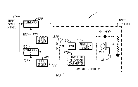
[0010] FIG. 1 is a functional diagram of a bidirectional low voltage
power supply (LVPS) in accordance with some embodiments. The bidirectional
low voltage power supply (LVPS) 100 may include a first converter 120
arranged to provide power from an input power source 110 to a load 190, and a
second converter 130 arranged to selectively recycle power from the load 190
at
an output of the first converter 120 back to the input power source 110. The
bidirectional low voltage power supply100 may also include control circuitry
140. The control circuitry may include, among other things, a single pulse
width
modulator (PWM) 160 and switching circuitry 175. The switching circuitry 175
may be configured to select either the first power converter 120 or the second
power converter 130 for reception of the output of the PWM 160.
2c
Date Recue/Date Received 2021-12-08

CA 02956260 2017-01-24
WO 2016/022932
PCT/US2015/044237
[0011] In these embodiments, the single bidirectional LVPS 100 may be
used to power the load 190 and recycle power returned from the load 190 back
to the input power source 110. This may increase system efficiency and may
reduce the thermal load. Unlike some conventional systems, the single PWM
160 is used to control both converters (i.e., converter 120 and converter
130). An
example of a bidirectional LVPS that uses two separate converters with each
converter having a PWM is described in U.S. Patent Application Serial No
13/855,295 [ref no. 12-29651 which is assigned to the same assignee as the
present application and which is incorporated herein by reference.
[0012] In some embodiments, the switching circuitry 175 may be
configured to selectively provide either a first gate drive signal 176 to the
first
power converter 120 or a second gate drive signal 177 to the second power
converter 130 to cause only one of the power converters 120 or 130 to operate
at
any one time. In these embodiments, the first converter 120 may be configured
to regulate voltage to the load 190 when the load 190 is sinking power and the
second converter 130 may be configured to regulate voltage to the load 190
when the load is sourcing power. In some motor drive and cryogenic cooler
embodiments, the first converter 120 is configured to regulate voltage to
motor
drive electronics when a motor is sinking power, and the second converter 130
is
configured to regulate voltage to the motor drive electronics when the motor
is
sourcing power, although the scope of the embodiments is not limited in this
respect.
[0013] In some embodiments, a first gate drive circuit 180 may be
configured to provide a gate drive signal 182 to drive one or more converter
switch transistors of the first power converter 120. A second gate drive
circuit
185 may be configured to provide a gate drive signal 187 to drive one or more
converter switch transistors of the second power converter 130. In some
embodiments, the first gate drive circuit 180 and/or the second gate drive
circuit
185 may be isolated gate drives, although the scope of the embodiments is not
limited in this respect.
[0014] In some embodiments, the switching circuitry 175 may be
arranged to cause the LVPS 100 to switch between operation of the first power
converter 120 to provide power from the input power source 110 to the load 190
3

CA 02956260 2017-01-24
WO 2016/022932
PCT/US2015/044237
and operation of the second power converter 130 to recycle power from the load
190 back to the input power source 110. In some embodiments, the input power
source 110 may be an input power bus, although the scope of the embodiments
is not limited in this respect.
[0015] In some embodiments, the control circuitry 140 may also
comprise an error amplifier 150, an absolute value circuit 155 and a converter
selection comparator 170. In these embodiments, the absolute value circuit 155
may be configured to provide the absolute value of the difference between the
output voltage of the error amplifier 150 and zero volts. The converter
selection
comparator 170 may be configured to cause the switching circuitry 175 to
switch
an output of the pulse width modulator 160 between the first power converter
120 and the second power converter 130. In some of these embodiments, the
regulated power supply output voltage and the reference voltage 151 may be any
suitable positive voltage, although the scope of the embodiments is not
limited in
this respect as other output voltages and reference voltages may be used. In
some
embodiments, the absolute value circuit 155 may be configured to provide a
signal into the PWM 160 equal to the difference between the output of the
error
amplifier 150 and a second reference voltage.
[0016] The control circuitry 140 illustrated in FIG. 1 is provided as
an
example configuration. Other configurations for the control circuitry 140 may
also be suitable for use in the bidirectional LVPS 100.
[0017] In some embodiments, the bidirectional LVPS 100 may be a
bidirectional motor driver LVPS configured to provide power to motor drive
electronics of a motor drive system. In these embodiments, the load 190 may
comprise the motor drive electronics and the motor, although the scope of the
enibodiments is not limited in this respect. In some embodiments, the first
converter 120 may be configured to regulate voltage to the motor drive
electronics when the motor is sinking power and the second converter 130 may
be configured to regulate voltage to the motor drive electronics when the
motor
is sourcing power. In some embodiments, the motor may be a cryogenic cooler
motor, although the scope of the embodiments is not limited in this respect.
In
some example embodiments, the bidirectional LVPS 100 may save up to 20
4

CA 02956260 2017-01-24
WO 2016/022932
PCT/US2015/044237
Watts or more over some conventional techniques which provides a significant
improvement in efficiency.
[0018] * Some embodiments are directed to a cryogenic cooler system.
In these embodiments, the cryogenic cooler system may include motor drive
electronics and a bidirectional motor driver LVPS 100 configured to provide
power to the motor drive electronics of a motor drive system. In these
embodiments, the bidirectional motor drive LVPS may comprise a first
converter 120 arranged to provide power from an input power source 110 to a
load comprising the motor drive electronics and a motor, a second converter
130
arranged to selectively recycle power from the load 190 at an output of the
first
converter 120 back to the input power source 110, and control circuitry 140
comprising a single PWM 160 and switching circuitry 175. In some
embodiments, the switching circuitry 175 may be configured to select either
the
first power converter 120 or the second power converter 130 for reception of
an
output of the PWM 160.
[0019] In some of these cryogenic cooler system embodiments, the
first
converter 120 may be configured to regulate voltage to the motor drive
electronics when the motor is sinking power and the second converter 130 may
be configured to regulate voltage to the motor drive electronics when the
motor
is sourcing power, although the scope of the embodiments is not limited in
this
respect. In some of these cryogenic cooler system embodiments, the switching
circuitry 175 may be configured to selectively provide either a first gate
drive
signal 176 to the first power converter 120 or a second gate drive signal 177
to
the second power converter 130 to cause only one of the power converters to
operate at the same time, although the scope of the embodiments is not limited
in
this respect.
[0020] FIG. 2 illustrates control circuitry in accordance with some
embodiments. Control circuitry 240 may be suitable for use as control
circuitry
140 in bidirectional I,VPS 100 (FIG. 1), although this is not a requirement as
other examples of control circuitry may also be suitable.
[0021] Control circuitry 240 may comprise a single PWM 260 and
switching circuitry 275 (i.e., a converter selection switch) that may be
configured to select either the first power converter 120 (FIG. 1) or the
second
5

CA 02956260 2017-01-24
WO 2016/022932
PCT/US2015/044237
power converter 130 (FIG. 1). In these embodiments, the switching circuitry
275
may selectively provide either a first gate drive signal 276 to the first
power
converter 120 or a second gate drive signal 277 to the second power converter
130 to cause only one of the power converters 120 or 130 to operate at a time.
[0022] In some embodiments, a first output 276 from the switching
circuitry 275 may be provided to the first gate drive circuit 180 (FIG. 1) and
a
second output 277 from the switching circuitry 275 may be provided to the
second gate drive circuit 185 (FIG. 1). In these embodiments, the first gate
drive
circuit 180 may provide the first gate drive signal 182 to drive one or more
converter switch transistors of the first power converter 120 and the second
gate
drive circuit 185 may provide a second gate drive signal 187 to drive one or
more converter switch transistors of the second power converter 130.
[0023] In some embodiments, the control circuitry 240 may also
comprise an error amplifier 250, an absolute value circuit 255 and a converter
selection comparator 270. In these embodiments, the absolute value circuit 255
may be configured to provide an absolute value of the difference between the
output of the error amplifier 250 and zero volts. The converter selection
comparator 270 may be configured to cause the switching circuitry 275 to
switch
an output of the pulse width modulator 260 between the first power converter
120 and the second power converter 130.
[0024] FIG. 3 illustrates a bidirectional low voltage power supply in
accordance with some other embodiments. The bidirectional low voltage power
supply 300 may be suitable for use as bidirectional low voltage power supply
100 (FIG. 1), although the scope of the embodiments is not limited in this
respect. In these embodiments, the first converter 320 may arranged to provide
power from the input power source 310 to the load 390, and the second
converter 330 may be arranged to selectively recycle power from the load 390
at
an output of the first converter 320 back to the input power source 310. The
control circuitry 340 may comprise a single PWM and switching circuitry that
may be configured to select either the first power converter 320 or the second
power converter 330 for reception of an output of the PWM.

CA 02956260 2017-01-24
WO 2016/022932
PCT/US2015/044237
[0025] In some embodiments, control circuitry 140 (FIG. 1) and/or
control circuitry 240 (FIG. 2) may be suitable for use as the control
circuitry 340
(FIG. 3), although this is not a requirement.
[0026] In some of these embodiments, a first output 176 from the
switching circuitry 175 (FIG. 1) may be provided to the first gate drive
circuit
180 (FIG. 1) and a second output 177 from the switching circuitry 175 may be
provided to the second gate drive circuit 185 (FIG. 1). In these embodiments,
the
first gate drive circuit 380 may provide the first gate drive signal 382 to
drive
one or more converter switch transistors of the first power converter 320 and
the
second gate drive circuit 385 may provide a second gate drive signal 387 to
drive
one or more converter switch transistors of the second power converter 330.
[0027] FIG. 4 illustrates a procedure for bidirectional low-voltage
power
supply operation in accordance with some embodiments. Procedure 400 may be
performed by a bidirectional low-voltage power supply, such as the
bidirectional
LVPS 100 (FIG. 1), although the scope of the embodiments is not limited is
this
respect as other bidirectional low-voltage power supply configurations may
also
be used.
[0028] Operation 402 may comprise providing, by a first converter 120
(FIG. 1) arranged to provide power from an input power source 110 (FIG. 1) to
a
load 190 (FIG. 1).
[0029] Operation 404 may comprise selectively recycling, by a second
converter 130 (FIG. 1), power from the load 190 at an output of the first
converter 120 back to the input power source 110.
[0030] Operation 406 may comprise selectively switching either the
first
power converter 120 or the second power converter 130 for reception of an
output of a single PWM 160 (FIG. 1). Operation 406 may be performed by
control circuitry, such as control circuitry 140 (FIG. 1).
[0031] Although the bidirectional low voltage power supply 100 (FIG.
1), the control circuitry 240 (FIG. 2) and the bidirectional low voltage power
supply 300 (FIG. 3) are illustrated as having several separate functional
elements, one or more of the functional elements may be combined and may be
implemented by combinations of digital electronics, such as digital PWMs,
firmware-configured or software-configured elements, such as processing
7

elements including digital signal processors (DSPs), and/or other hardware
elements. For example, some elements may comprise one or more
microprocessors, DSPs, field-programmable gate arrays (FPGAs), application
specific integrated circuits (ASICs), and combinations of various hardware and
logic circuitry for performing at least the functions described herein. In
some
embodiments, the functional elements may refer to one or more processes
operating on one or more processing elements.
[0032] Embodiments may be implemented in one or a combination of
hardware, firmware and software. Embodiments may also be implemented as
instructions stored on a computer-readable storage device, which may be read
and executed by at least one processor to perform the operations described
herein. A computer-readable storage device may include any non-transitory
mechanism for storing information in a form readable by a machine (e.g., a
computer). For example, a computer-readable storage device may include read-
only memory (ROM), random-access memory (RAM), magnetic disk storage
media, optical storage media, flash-memory devices, and other storage devices
and media. Some embodiments may include one or more processors and may be
configured with instructions stored on a computer-readable storage device.
8
Date Recue/Date Received 2021-12-08

Dessin représentatif
Une figure unique qui représente un dessin illustrant l'invention.
États administratifs

2024-08-01 : Dans le cadre de la transition vers les Brevets de nouvelle génération (BNG), la base de données sur les brevets canadiens (BDBC) contient désormais un Historique d'événement plus détaillé, qui reproduit le Journal des événements de notre nouvelle solution interne.

Veuillez noter que les événements débutant par « Inactive : » se réfèrent à des événements qui ne sont plus utilisés dans notre nouvelle solution interne.

Pour une meilleure compréhension de l'état de la demande ou brevet qui figure sur cette page, la rubrique Mise en garde , et les descriptions de Brevet , Historique d'événement , Taxes périodiques et Historique des paiements devraient être consultées.

Historique d'événement

Description Date
Inactive : Octroit téléchargé 2023-08-29
Lettre envoyée 2023-08-29
Accordé par délivrance 2023-08-29
Inactive : Octroit téléchargé 2023-08-29
Inactive : Page couverture publiée 2023-08-28
Préoctroi 2023-06-20
Inactive : Taxe finale reçue 2023-06-20
Lettre envoyée 2023-03-01
Un avis d'acceptation est envoyé 2023-03-01
Inactive : Q2 réussi 2022-12-13
Inactive : Approuvée aux fins d'acceptation (AFA) 2022-12-13
Modification reçue - modification volontaire 2022-06-24
Modification reçue - réponse à une demande de l'examinateur 2022-06-24
Rapport d'examen 2022-06-10
Demande d'entrevue reçue 2022-06-06
Inactive : Rapport - Aucun CQ 2022-06-06
Modification reçue - réponse à une demande de l'examinateur 2021-12-08
Modification reçue - modification volontaire 2021-12-08
Rapport d'examen 2021-08-12
Inactive : Rapport - Aucun CQ 2021-07-30
Représentant commun nommé 2020-11-07
Lettre envoyée 2020-07-13
Exigences pour une requête d'examen - jugée conforme 2020-06-30
Requête d'examen reçue 2020-06-30
Toutes les exigences pour l'examen - jugée conforme 2020-06-30
Représentant commun nommé 2019-10-30
Requête pour le changement d'adresse ou de mode de correspondance reçue 2019-07-24
Exigences relatives à la nomination d'un agent - jugée conforme 2018-05-01
Exigences relatives à la révocation de la nomination d'un agent - jugée conforme 2018-05-01
Demande visant la nomination d'un agent 2018-04-27
Demande visant la révocation de la nomination d'un agent 2018-04-27
Inactive : Page couverture publiée 2017-08-11
Inactive : CIB en 1re position 2017-03-15
Inactive : CIB attribuée 2017-03-15
Inactive : CIB enlevée 2017-03-15
Inactive : CIB attribuée 2017-03-15
Inactive : Notice - Entrée phase nat. - Pas de RE 2017-02-06
Inactive : CIB attribuée 2017-01-30
Demande reçue - PCT 2017-01-30
Exigences pour l'entrée dans la phase nationale - jugée conforme 2017-01-24
Demande publiée (accessible au public) 2016-02-11

Historique d'abandonnement

Il n'y a pas d'historique d'abandonnement

Taxes périodiques

Le dernier paiement a été reçu le 2023-07-21

Avis : Si le paiement en totalité n'a pas été reçu au plus tard à la date indiquée, une taxe supplémentaire peut être imposée, soit une des taxes suivantes :

  • taxe de rétablissement ;
  • taxe pour paiement en souffrance ; ou
  • taxe additionnelle pour le renversement d'une péremption réputée.

Les taxes sur les brevets sont ajustées au 1er janvier de chaque année. Les montants ci-dessus sont les montants actuels s'ils sont reçus au plus tard le 31 décembre de l'année en cours.
Veuillez vous référer à la page web des taxes sur les brevets de l'OPIC pour voir tous les montants actuels des taxes.

Historique des taxes

Type de taxes Anniversaire Échéance Date payée
Taxe nationale de base - générale 2017-01-24
TM (demande, 2e anniv.) - générale 02 2017-08-07 2017-07-25
TM (demande, 3e anniv.) - générale 03 2018-08-07 2018-07-12
TM (demande, 4e anniv.) - générale 04 2019-08-07 2019-07-25
Requête d'examen - générale 2020-08-07 2020-06-30
TM (demande, 5e anniv.) - générale 05 2020-08-07 2020-07-06
TM (demande, 6e anniv.) - générale 06 2021-08-09 2021-07-21
TM (demande, 7e anniv.) - générale 07 2022-08-08 2022-07-20
Taxe finale - générale 2023-06-20
TM (demande, 8e anniv.) - générale 08 2023-08-07 2023-07-21
Titulaires au dossier

Les titulaires actuels et antérieures au dossier sont affichés en ordre alphabétique.

Titulaires actuels au dossier
RAYTHEON COMPANY
Titulaires antérieures au dossier
JOE ANTHONY ORTIZ
Les propriétaires antérieurs qui ne figurent pas dans la liste des « Propriétaires au dossier » apparaîtront dans d'autres documents au dossier.
Documents

Pour visionner les fichiers sélectionnés, entrer le code reCAPTCHA :


Pour visualiser une image, cliquer sur un lien dans la colonne description du document. Pour télécharger l'image (les images), cliquer l'une ou plusieurs cases à cocher dans la première colonne et ensuite cliquer sur le bouton "Télécharger sélection en format PDF (archive Zip)" ou le bouton "Télécharger sélection (en un fichier PDF fusionné)".

Liste des documents de brevet publiés et non publiés sur la BDBC .

Si vous avez des difficultés à accéder au contenu, veuillez communiquer avec le Centre de services à la clientèle au 1-866-997-1936, ou envoyer un courriel au Centre de service à la clientèle de l'OPIC.


Description du
Document 
Date
(aaaa-mm-jj) 
Nombre de pages   Taille de l'image (Ko) 
Dessin représentatif 2023-08-07 1 13
Description 2017-01-23 8 344
Dessin représentatif 2017-01-23 1 12
Revendications 2017-01-23 6 173
Dessins 2017-01-23 2 48
Abrégé 2017-01-23 1 64
Revendications 2021-12-07 10 398
Description 2021-12-07 11 518
Revendications 2022-06-23 10 547
Avis d'entree dans la phase nationale 2017-02-05 1 194
Rappel de taxe de maintien due 2017-04-09 1 111
Courtoisie - Réception de la requête d'examen 2020-07-12 1 432
Avis du commissaire - Demande jugée acceptable 2023-02-28 1 580
Taxe finale 2023-06-19 4 137
Certificat électronique d'octroi 2023-08-28 1 2 528
Rapport de recherche internationale 2017-01-23 2 53
Demande d'entrée en phase nationale 2017-01-23 4 109
Requête d'examen 2020-06-29 4 135
Demande de l'examinateur 2021-08-11 5 238
Modification / réponse à un rapport 2021-12-07 23 928
Note d'entrevue avec page couverture enregistrée 2022-06-05 1 15
Demande de l'examinateur 2022-06-09 3 136
Modification / réponse à un rapport 2022-06-23 15 519