Note : Les descriptions sont présentées dans la langue officielle dans laquelle elles ont été soumises.
CA 02970420 2017-06-09
WO 2015/087089 PCT/GB2014/053695
1
Title - Improvements relating to Power Adaptors
This invention relates to power adaptors, and particularly to power adaptors
for
providing compatibility between a power reducing device powered from an AC
power supply and a load, such as a light source, with a significantly lower
power rating than that required to maintain compatibility.
LEDs are light sources that are being developed to replace conventional
lighting systems, such as fluorescent and incandescent lights, in order to
1.0 provide more energy efficient systems. Since an incandescent light
source
typically consumes 60-100W and has a short lifetime, an LED bulb would be
the excellent substitute with considerably less power dissipation and longer
life.
There has therefore been much research into the development of an LED bulb
compatible with TRIAC dimmers, which are common in lighting systems.
A major issue with TRIAC dimmable LED bulbs is dimmer compatibility. The
conventional TRIAC dimmer was designed to handle hundreds of watts induced
by incandescent bulbs. An LED bulb consuming much less power will interact
with those dimmers composed of high-power devices. If the interaction
between dimmer and LED bulb is not stabilized, visible flicker is perceptible.
In order to prevent visible flicker, a conventional TRIAC dimmer needs a
latching current at firing and a holding current during the TRIAC turn-on
after
firing. If those two currents are not met, the TRIAC dimmer misfires and the
LED light source flickers.
The latching and holding currents are different between different dimmer
models. The typical range of latching and holding currents is around 5 - 50
mA.
Those operating requirements do not cause problems when incandescent bulbs
are used, due to their high power consumption. However, an LED bulb with
much less output power cannot maintain this amount of current over the whole
line cycle without additional circuitry.
CA 02970420 2017-06-09
WO 2015/087089 PCT/GB2014/053695
2
Conventional power adaptors typically require a second stage that provides
compatibility, but this increases costs. It is also known to regulate the LEDs
themselves in an attempt to reduce or eliminate flicker, even though the power
supply is unstable.
There have now been devised improved power adaptors which overcome or
substantially mitigate the above-mentioned and/or other disadvantages
associated with the prior art.
According to a first aspect of the invention, there is provided a power
adaptor
comprising an input for connection to an AC power supply, an output for
connection to a load, and a resonant circuit coupled to the input that
provides
power to the output suitable for driving the load, wherein the power adaptor
includes a controller adapted to drive the resonant circuit in two or more
different modes to select different characteristics of the current drawn from
the
AC power supply, in use.
According to a further aspect of the invention, there is provided a controller
for
use with a power adaptor comprising an input for connection to an AC power
supply, an output for connection to a load, and a resonant circuit coupled to
the
input that provides power to the output suitable for driving the load, the
controller being adapted to drive the resonant circuit in two or more
different
modes to select different characteristics of the current drawn from the AC
power supply, in use.
According to a further aspect of the invention, there is provided a power
adaptor
comprising an input for connection to an AC power supply, an output for
connection to a load, and a resonant circuit coupled to the input that
provides
power to the output suitable for driving the load, the resonant circuit having
two
or more resonant frequencies, which are not harmonics of each other, wherein
the power adaptor includes a controller adapted to drive the resonant circuit
at,
CA 02970420 2017-06-09
WO 2015/087089
PCT/GB2014/053695
3
or near, each of the two or more resonant frequencies to select different
characteristics of the current drawn from the AC power supply, in use.
According to a further aspect of the invention, there is provided a controller
for
use with a power adaptor comprising an input for connection to an AC power
supply, an output for connection to a load, and a resonant circuit coupled to
the
input that provides power to the output suitable for driving the load, the
resonant circuit having two or more resonant frequencies, which are not
harmonics of each other, the controller being adapted to drive the resonant
circuit at, or near, each of the two or more resonant frequencies to select
different characteristics of the current drawn from the AC power supply, in
use.
The load may be a light source, for example a solid state light source. The
controller may be programmed to drive the resonant circuit at, or near, each
of
the two or more resonant frequencies to select different characteristics of
the
current drawn from the AC power supply, in use, eg without user input. The
controller may be programmed to drive the resonant circuit according to
programmed actions and/or in response to one or more inputs.
The controller may be adapted to drive the resonant circuit at, or near, a
plurality of the two or more resonant frequencies within an AC cycle, eg
within
an AC half-cycle. The controller may be adapted to drive the resonant circuit
at, or near, a plurality of the two or more resonant frequencies within each
AC
cycle, eg within each AC half-cycle, in a selected mode of the controller.
The controller may be adapted to detect a power reducing device of the AC
power supply and select a pre-determined current profile for determining the
characteristics of the current to be drawn from the AC power supply.
The power adaptor may have a current profile, for example for use with a
stable, leading edge, eg TRIAC, dimmer switch, that draws current for the time
that the dimmer switch is turned on, or a substantial part thereof.
CA 02970420 2017-06-09
WO 2015/087089
PCT/GB2014/053695
4
The power adaptor may have a current profile, for example for use with an
unstable, leading edge, eg TRIAC, dimmer switch, that draws current for a pre-
determined time period during an intermediate portion of the half-cycle of the
AC power supply. In particular, the intermediate portion of the half-cycle of
the
AC power supply may be separated from the zero crossings, and may be a
portion when the voltage is sufficiently high for the TRIAC to be stable. The
current drawn may be at a higher level than that drawn in another current
profile, eg a current profile for a stable dimmer switch. This may be achieved
by utilising a second resonant frequency of the resonant circuit for a pre-
determined time period, which causes a greater current to be drawn by the
lamp.
The pre-determined time period during which current is drawn may be shorter
than the time period during which current is drawn in another current profile,
eg
a current profile for a stable dimmer switch, in order to maintain the power
output to the LED sufficiently low to ensure that the lamp does not overheat.
In
particular, the current profiles may be adapted such that the power outputs
are
substantially the same across a half- or full-cycle.
A current profile for use with an unstable, leading edge, eg TRIAC, dimmer
switch may be entered when instability is detected. The power adapter may be
adapted to monitor the resonant waveform, so as to detect variations in that
waveform. Variations in the resonant waveform may have the form of gaps,
rapid changes or other variations. The presence or absence of variations in
the
resonant waveform may be indicative of the type of power reducing device, eg
dimmer switch, to which the power adapter is connected. The presence of
gaps, variations or rapid changes in the resonant waveform may be indicative
of false triggers and the presence of an unstable leading edge (eg TRIAC)
dimmer. Any gaps, variations or rapid changes in the resonant waveform can
be detected within 1-3 mains half cycles, such that the suitable current
profile is
CA 02970420 2017-06-09
WO 2015/087089
PCT/GB2014/053695
activated quickly, with the result that flickering of the lamp is
imperceptible by
the human eye.
For the leading edge current profiles, the power adaptor may create a load
5 condition when the switch of the power reducing device, eg the TRIAC of
the
dimmer switch, fires for a pre-determined period, eg for approximately 300ps,
in
order to facilitate latching of the TRIAC of the dimmer switch. This load
condition may be achieved by overlapping the on-times of the high- and low-
side switches of a half-bridge drive for the resonant circuit. The current
drawn
1.0 during this load condition may be greater than the current drawn in the
remainder of the cycle, eg at least twice magnitude. The current drawn during
the period of the load condition may reduce, eg gradually. For example, the
current may initially be at least twice the magnitude of the current drawn in
the
remainder of the cycle, and this current may reduce to the current drawn in
the
remainder of the cycle during the time period of the load condition.
The power adaptor may have a current profile, for example for use with a
constant mains supply, or a trailing edge dimmer switch, that draws current
for
the time that the dimmer switch is turned o, or a substantial portion thereof.
For
zo trailing edge dimmer switches, it may be necessary to draw a greater
current
once the dimmer switch turns off, in order to discharge the dimmer switch in a
sufficiently short period of time. This may be achieved by utilising a second
resonant frequency of the resonant circuit for a pre-determined time period,
which causes a greater current to be drawn by the lamp. Alternatively, a load
condition may be created, for example by overlapping the on-times of the high-
and low-side switches of a half-bridge drive for the resonant circuit.
The power adaptor may have a current profile, for example for use with an
unstable, leading edge, eg TRIAC, dimmer switch that stops drawing current
following an initial time period following firing of the TRIAC of a dimmer
switch,
eg once current inrush has collapsed, thereby turning off the TRIAC of the
dimmer. The initial period may be a pre-determined time period, eg 300ps.
CA 02970420 2017-06-09
WO 2015/087089
PCT/GB2014/053695
6
The inrush current may charge an energy storage device, eg one or more
capacitors, which provide power to the output once the TRIAC of the dimmer
has been turned off.
The provision of power to the output may continue until the TRIAC of the
dimmer turns back on, which may be detected by detecting a change, eg a
sharp rise, in the input voltage. The power adaptor may cease providing power
to the output during the time period in which the TRIAC of the dimmer is
turned
on.
This allows TRIAC dimmers that have very high latch and hold current
requirements (eg 1000W) to dim very low power LEDs (eg 5W) without visible
flicker. In particular, this allows the use of a single stage power adaptor,
eg a
resonant power adaptor, which is less expensive than power adaptors having a
second stage to regulate out flicker.
This current profile is considered to be novel and inventive in itself and,
hence,
according to a further aspect of the invention, there is provided a power
adaptor
comprising an input for connection to an AC power supply including a power
reducing device, an output for connection to a load, an energy storage device
coupled to the input, and a resonant circuit coupled to the input that
provides
power to the output suitable for driving the load, wherein the power adaptor
includes a controller adapted to detect activation of a switch in the power
reducing device of the AC power supply and reduce the current drawn from the
AC power supply to deactivate said switch, the energy storage device providing
power to the output in a period during which the switch of the power reducing
device is deactivated.
The load may be a light source, for example a solid state light source.
CA 02970420 2017-06-09
WO 2015/087089 PCT/GB2014/053695
7
The resonant circuit may have a resonant frequency at which it is able to
maintain a substantially constant current input for varying input voltages.
The
resonant circuit may therefore be an LCL series-parallel resonant circuit. An
LCL series-parallel resonant circuit comprises a first inductor L1 and a first
capacitor Cl in series, and a parallel load leg including a second inductor
L2.
The first inductor L1 and first capacitor Cl are connected in series between
two
input terminals of the resonant circuit, and the load leg is connected in
parallel
across the first capacitor Cl, wherein the load leg comprises the second
inductor L2 and an output for driving the load, which are connected in series.
Power adaptors utilising an LCL series-parallel resonant circuit are described
in
WO 2008/120019, WO 2010/041067, WO 2010/139992, WO 2011/083336 and
WO 2012/010900, the teaching of each of which are incorporated herein by
reference in their entirety.
The use of an LCL series-parallel resonant circuit provides a power adaptor
suitable for solid state light sources, such as LEDs, that has a substantially
constant current draw and high efficiency. In particular, the output current
becomes independent of output voltage and if the power adaptor is powered by
a low frequency sine voltage input, and the output voltage is constant, ie an
LED load, the input current becomes a low frequency, substantially square
wave ideal for drive by a TRIAC dimmer as it maintains the hold current at the
lowest possible power whilst providing the LED with a current source that
varies
in brightness with the low frequency input voltage, ie it makes the LED act
like a
lamp bulb and enables control by a TRIAC dimmer at vastly reduced power and
high power factor relative to other power adaptor technology.
The load may therefore be one or more LEDs, and the input may be drawn from
a TRIAC or SCR dimmer.
The LCL series-parallel circuit may be adapted to have at least two resonant
frequencies, a first resonant frequency that provides, at a given input
voltage, a
CA 02970420 2017-06-09
WO 2015/087089 PCT/GB2014/053695
8
constant current output that is independent of the load, and a second resonant
frequency that provides, at a given input voltage, a current that varies with
load.
An LCL series-parallel circuit will also have a third resonant frequency at
0Hz,
ie DC current.
These resonant frequencies may be achieved by selecting the first inductor,
the
second inductor and the first capacitor, such that the reactances of those
components are substantially equal. The second resonant frequency may be
adapted to provide a significantly greater power at the output, relative to
the first
lo resonant frequency. A controller of the power adaptor may therefore be
adapted to switch between the different resonant frequencies in order to
utilise
their different characteristics.
The resonant circuit may be driven by a resonance drive circuit, which
provides
a resonance drive signal to the resonant circuit. The resonance drive signal
is
preferably an alternating signal, and is preferably provided by an oscillator
that
may control two or four electronic switches, eg FETs. The resonance drive
signal typically has the form of a square wave. The purpose of the drive
circuit
is to excite the resonant circuit with an alternating voltage, the alternating
voltage typically consisting of blocks of positive and negative voltage. The
electronic switches are typically connected together in the form of a full
bridge
inverter (4 switches) or a half bridge inverter (2 switches).
The power adaptor may be adapted to modify the waveform of the current that
would inherently be drawn by the resonant circuit, and in particular modify
the
shape and/or size of that waveform. In particular, a resonance drive signal
may
be provided to the resonant circuit, wherein the resonance drive signal is
adapted to determine the desired input current waveform. For instance, the
power adaptor may comprise at least one half-bridge drive circuit for
providing a
drive signal to the resonant circuit, and a switch controller for the half-
bridge
drive circuit, the half-bridge drive circuit having a high-side switch and a
low-
side switch. The switch controller may be adapted to provide one or more of
CA 02970420 2017-06-09
WO 2015/087089
PCT/GB2014/053695
9
the following, in at least one mode: (i) to provide the high-side switch and
the
low-side switch with on-times of different durations, (ii) to provide the high-
side
switch and the low-side switch with on-times that overlap, and (iii) to
provide the
high-side switch and the low-side switch with on-times that are synchronous.
The high-side switch and the low-side switch having on-times of different
durations may be utilised to control the current drawn from the input. In
particular, the high-side switch and the low-side switch may have on-times of
different durations, ie asymmetric on-times, such that the degree of asymmetry
lo between the high-side switch and the low-side switch determines the
current
drawn from the input. It has been found that the greater the degree of
asymmetry between the on-times of the high-side switch and the low-side
switch, the less current drawn from the input.
The current drawn at the input may be substantially equal to the current
provided at the output, for example if there is no overlap between the on-
times
of the high- and low-side switches. This enables dimming control effected by
the switch controller, without the need to change the frequency at which the
resonant circuit is driven, and therefore without any need to change the
resonant circuit itself. In particular, in order to reduce the current drawn
from
the input and the current provided at the output, the on-times of the high-
side
switch and the low-side switch may be varied relative to each other, for
example such that the on-time of the high-side switch is shorter than the on-
time of the low-side switch.
The high-side switch and the low-side switch having on-times of different
durations, ie asymmetric on-times, may be utilised to determine the waveform
of the current drawn at the input, eg to provide dimmer compatibility and/or
reduce harmonic distortion. In particular, this may be achieved by the switch
controller providing the high-side switch and the low-side switch with on-
times
of different durations, ie asymmetric on-times, and varying the degree of
CA 02970420 2017-06-09
WO 2015/087089
PCT/GB2014/053695
asymmetry between the high-side switch and the low-side switch during each
input cycle to determine the waveform of the current drawn from the input.
An overlap between the on-times of the switches may be utilised to create a
5 load condition in the period of overlap, in each input cycle, which may
increase
the current drawn at the input relative to the current delivered to the output
in
the period of overlap, in each input cycle. This enables the current at the
output
to be reduced without reducing the current drawn at the input, for example. In
addition, it enables a latch current for a dimmer switch to be drawn in each
10 input cycle, in the period of overlap, and a lower hold current to be
drawn
subsequently, in each input cycle, without any need to change the frequency at
which the resonant circuit is driven. Since the latch current for a
conventional
dimmer switch in a mains supply (eg 85mA) typically only needs to be drawn for
a few hundred us, relative to the hold current (eg 50mA) that is typically
drawn
for a few ms, the additional current (35mA) that is not provided to the output
would result in acceptably small losses, eg 100-200mW on 230V mains supply.
This control may also help reduce the voltage reduction problems seen just
after the TRIAC of a conventional dimmer switch fires, and may therefore
negate the need for snubber circuits and their associated losses.
The power adaptor may also have a mode in which no power is provided at the
output, but the power adaptor provides a load condition to the input, by the
switch controller providing the high-side switch and the low-side switch with
simultaneous on-times.
The greater the duration of the overlap for the on-times or the duration of
the
simultaneous on-times, the lower the resistance or dynamic impedance of the
load provided. This is particularly advantageous for solid state light
sources, eg
LEDs. In particular, this load condition may provide a DC path, which prevents
false start-up conditions. This enables use with dimmers, and also prevents
glowing occurring from a pickup supply.
CA 02970420 2017-06-09
WO 2015/087089
PCT/GB2014/053695
11
The switch controller may utilise any combination of the above configurations
of
on-times to provide the desired current draw at the input and the required
current at the output.
Where the power adaptor has a mode in which a load condition is generated by
overlapping or synchronous on-times of the switches, the controller may be
adapted to determine whether the impedance of the load condition will be
acceptable for the voltage of the power supply. The controller is preferably,
therefore, adapted to monitor the voltage of the power supply.
The power adaptor may be adapted to switch between two or more modes,
which each provide a different configuration of on-times for the high-side
switch
and the low-side switch. Since the present invention enables different modes
without changing the frequency at which the resonant circuit is driven, the
resonant circuit is preferably driven at, or approximately at, its resonant
frequency or a sub-harmonic thereof in each mode.
The power adaptor may be adapted to monitor the input voltage, and alter the
ratio between the current provided at the output and the resistance across the
zo input, based on that input voltage. In particular, this ratio may be
altered
proportionally based on the input voltage, such that sudden changes in current
and/or input resistance are not created when switching modes. Where the
power adaptor is adapted for use with a mains supply and solid state light
sources, these sudden changes in current and/or input resistance may cause
ringing or harmonics on the mains, possible flicker on the output, and may
result in dimmer incompatibility. The ratio may be altered by changing the
amount of overlap of the on-times of the high- and low-side switches.
The high- and low-side switches are preferably bipolar junction transistors
(BJTs), which are typically less expensive than field-effect transistors
(FETs).
Furthermore, since BJTs have limited gain, there is a reduced risk of damage
to
CA 02970420 2017-06-09
WO 2015/087089
PCT/GB2014/053695
12
the switches from current inrush relative to FETs, which have infinite gain
and
require damping circuits.
In presently preferred embodiments, the high-side switch and the low side
switch of the half-bridge drive circuit are arranged with their respective
emitter
or source terminals connected at the centre of the half bridge.
Since, in this embodiment, the switching voltage applied to the base or gate
terminal of a transistor is referenced relative to the voltage at the emitter
or
io source terminal, this enables a common reference in the form of a
floating
ground. This removes any need for a level shifter circuit, which is a high
voltage circuit that is typically expensive and results in power loss, and
hence
reduced efficiency. The invention therefore reduces cost and increases
efficiency relative to the prior art. In addition, the invention enables the
drive
is circuitry to be at low voltage, and enables the same drive circuitry to
drive both
the high- and low-side switches.
The high-side switch is preferably an NPN bipolar junction transistor (BJT),
or a
similarly functioning transistor. The low-side switch is preferably a PNP
bipolar
20 junction transistor (BJT), or a similarly functioning transistor. The
transistors
being bipolar junction transistors (BJTs) may enable the switch controller to
be
at low voltage, eg less than 5V, eg 2V. Where an integrated circuit is
provided,
a low voltage power supply may be formed by one or more diodes and an
energy storage device such as a capacitor.
The switches are typically configured with a switching voltage at the base or
gate terminal that is determined relative to the voltage at the emitter or
source
terminal. The connection between the emitter or source terminals of the high-
side switch and the low side switch preferably therefore provides a common
reference for the switching voltage of the high-side switch and the low-side
switch in the form of a floating ground. The collector or drain terminals of
the
CA 02970420 2017-06-09
WO 2015/087089
PCT/GB2014/053695
13
high-side switch and the low side switch may be connected to the positive
supply voltage and normal ground, eg OV, respectively, of the circuit.
The low-side switch preferably has a negative switching voltage at the
base/gate of the switch that is determined relative to a common reference in
the
form of a floating ground. The negative switching voltage may be generated by
a charge-pump, for example.
The switch controller preferably takes the form of an integrated circuit. The
1.0 ground connection of the switch controller is preferably connected to
the emitter
or source terminals of the high-side switch and the low side switch, such that
the ground connection of the switch controller has a reference common to the
high-side switch and the low side switch in the form of a floating ground.
The switch controller is preferably provided with a local supply, or a
bootstrap
from the normal ground, or the capacitors that would typically be connected
across the high- and low-side switches may be adapted to provide power to the
switch controller, these may feed the charge pump diodes on the
microprocessor.
This embodiment of the invention is particularly advantageous when used to
drive an LCL series-parallel resonant circuit. This arrangement enables the
half-bridge drive circuit to function without any feedback, eg from an
inductor to
an oscillator drive. This arrangement also removes the need for any feedback
transformers, which are large and expensive. The present invention is also
particularly advantageous to the LCL circuit as it allows the use of a low
voltage
process.
According to a further aspect of the invention, there is provided a lighting
unit
suitable for direct connection to a mains supply, the lighting unit comprising
a
power adaptor as described above and one or more non-solid state light
sources.
CA 02970420 2017-06-09
WO 2015/087089 PCT/GB2014/053695
14
The dimmer circuit preferably includes one or more silicon-controlled
rectifiers
(SCRs), or a TRIAC.
Example embodiments of the invention will now be described in detail, by way
of illustration only, with reference to the accompanying drawings, in which
Figure 1 shows a switch controller and a half-bridge drive circuit of an
embodiment of the power adaptor according to the invention;
1.0
Figure 2 shows an LCL series-parallel resonant circuit and DC link capacitors
of
an embodiment of the power adaptor according to the invention; and
Figures 3-6 illustrate the voltages and currents associated with first,
second,
third and fourth modes of the power adaptor according to the invention, across
a half-cycle.
An embodiment of a power adaptor according to the invention comprises an
input rectifier stage (not shown in the Figures), a switch controller (RAIS-
DH)
and a half bridge drive circuit (HSD,LSD) (shown in Figure 1), and an LCL
series-parallel resonant circuit (L1,C1,L2) and an output rectifier stage
(shown
in Figure 2). The high-side switch, 01, is an NPN BJT transistor, and the low-
side switch, 02, is PNP BJT transistor. 01 and 02 are arranged with their
emitters/sources connected to a common point, which forms a floating ground
for both 01 and 02. This common point also provides the output of the half-
bridge drive circuit which, in this embodiment, is fed to an LCL series-
parallel
resonant circuit suitable for driving a solid state light source (of the form
described in detail in GB 2449616 B8 and WO 2010/041067 Al).
01 and 02 are each switched by providing a switching pulse to the respective
base/gate, the voltage of the switching pulse being referenced to the
emitter/source of the switch. When 01 is switched on, the floating ground will
CA 02970420 2017-06-09
WO 2015/087089
PCT/GB2014/053695
be at the positive supply voltage, eg 330V, and the voltage at the base/gate
of
01 will be positive typ relative to the floating ground and hence the
emitter/source voltage. When 02 is switched on, the floating ground will be at
normal ground, eg OV, and the voltage at the base/gate of Q1 will be negative
5 relative to the floating ground and hence the emitter/source voltage.
The switches Q1 and 02 are driven by a switch controller, which is an
integrated circuit designated RAIS-DH, that is also referenced to the floating
ground. Since the switch controller RAIS-DH is driving BJT transistors, which
io require +-0.7V, the switch controller can be powered at 2V. In order to
switch
on 01, the switch controller provides a positive pulse to the base/gate of Ql,
relative to the floating ground (at the positive supply voltage, eg 330V) and
hence the emitter/source voltage. In order to switch on 02, the switch
controller provides a negative pulse to the base/gate of 02, relative to the
is floating ground (at normal ground, eg OV) and hence the emitter/source
voltage.
01 forms the high-side drive (HSD) and 02 forms the low-side drive (LSD) for
an LCL series-parallel resonant circuit (shown in Figure 2), which provides an
output suitable for driving a solid state light source. The switch controller
is
zo configured to manipulate the current drawn at the input, the current
delivered to
the output, and/or the impedance of the power adaptor, by controlling the on-
times of the high-side drive (HSD) and the low-side drive (LSD).
The output of the resonant circuit is rectified using a diode bridge, and then
smoothed by a capacitor at the output of the rectifier, so as to form an
output
suitable for driving the LED. The capacitors C5 and C6 create a connection
point for the second end of the resonant circuit, substantially midway in
voltage
between DC+ and OV.
The LCL series-parallel resonant circuit is configured such that it has two
non-
zero resonant frequencies.
CA 02970420 2017-06-09
WO 2015/087089
PCT/GB2014/053695
16
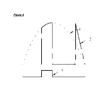
Figures 3-6 illustrate the voltages and currents associated with first,
second,
third and fourth modes of the power adaptor according to the invention, across
a half-cycle. In particular, a first trace (1) illustrates the voltage of the
mains
supply as seen before the dimmer switch, which is generally sinusoidal in
form.
A second trace (2) illustrates the voltage output from the dimmer switch,
which
is the input voltage of the lamp. A third trace (3) is the current drawn from
the
mains supply by the lamp.
In Figure 3, a first mode is illustrated for use with an unstable, leading
edge, eg
1.0 TRIAC, dimmer switch.
In this mode, the controller stops the power adaptor drawing current following
a
pre-determined time period of 30011s following firing of the TRIAC of the
dimmer
switch, ie once the current inrush has collapsed, thereby turning off the
TRIAC
of the dimmer. The inrush current drawn by the power adaptor in this period
charges the DC link capacitors. Following a pre-determined period of time
during which no power is delivered to the lamp (indicated by reference numeral
4 in Figure 3), which is sufficient to allow the TRIAC to turn off, the power
adaptor provides power from the DC link capacitors to the output and the lamp.
zo In particular, the lamp draws a constant current once the TRIAC has
turned off.
The provision of power to the output continues until the TRIAC of the dimmer
switch turns back on, which is detected by detecting a sharp rise in the input
voltage.
This allows TRIAC dimmers that have very high latch and hold current
requirements (eg 1000W) to dim very low power LEDs (eg 5W) without visible
flicker. In particular, this allows the use of a single stage power adaptor,
eg a
resonant power adaptor, which is less expensive than power adaptors having a
second stage to regulate out flicker.
In Figure 4, a second mode is illustrated for use with an unstable, leading
edge,
eg TRIAC, dimmer switch.
CA 02970420 2017-06-09
WO 2015/087089 PCT/GB2014/053695
17
In this mode, the power adaptor and lamp draw current for a pre-determined
time period during the half-cycle, when the voltage is sufficiently high for
the
TRIAC to be stable. The current drawn may be at a higher level than that
drawn for a stable dimmer switch. This may be achieved by utilising a second
resonant frequency of the resonant circuit for a pre-determined time period,
which causes a greater current to be drawn by the lamp.
The pre-determined time period during which current is drawn is shorter than
the time period during which current is drawn in the stable mode, in order to
maintain the power output to the LED at the same level as that in the other
modes, thereby ensuring that the lamp does not overheat.
This mode is entered when instability is detected. The power adapter is
adapted to monitor the resonant waveform, so as to detect variations in that
waveform that indicate instability. Variations in the resonant waveform may
have the form of gaps, rapid changes or other variations, which are indicative
of
false triggers and the presence of an unstable leading edge (eg TRIAC)
dimmer. This feature may enable a circuit that directly monitors the input
voltage to be omitted. In addition, any gaps, variations or rapid changes in
the
resonant waveform can be detected within 1-3 mains half cycles, such that the
suitable mode of operation is activated quickly, with the result that
flickering of
the lamp is imperceptible by the human eye.
In addition, although not shown in Figure 4, the power adaptor also creates a
load condition for a pre-determined period, eg for approximately 3001is, when
the TRIAC fires, in order to facilitate latching of the TRIAC of the dimmer
switch. This load condition is achieved by overlapping the on-times of the
high-
and low-side switches (HSD,LSD) of the half-bridge drive for the resonant
circuit. The current drawn during this load condition is initially 2-3 times
the
magnitude of the current drawn in the remainder of the cycle, and this current
CA 02970420 2017-06-09
WO 2015/087089
PCT/GB2014/053695
18
reduces gradually during the period of the load condition to the current drawn
in
the remainder of the cycle.
In Figure 5, a third mode is illustrated for use with a stable, leading edge,
eg
TRIAC, dimmer switch.
In this mode, the power adaptor enables the lamp to draw current for the
entire
time period during which the dimmer switch is turned on.
In addition, although not shown in Figure 4, the power adaptor also creates a
load condition for a pre-determined period, eg for approximately 300 s, when
the TRIAC fires, in order to facilitate latching of the TRIAC of the dimmer
switch. This load condition is achieved by overlapping the on-times of the
high-
and low-side switches (HSD,LSD) of the half-bridge drive for the resonant
circuit. The current drawn during this load condition is initially 2-3 times
the
magnitude of the current drawn in the remainder of the cycle, and this current
reduces gradually during the period of the load condition to the current drawn
in
the remainder of the cycle.
In Figure 6, a fourth mode is illustrated for use with a trailing edge dimmer
switch.
In this mode, the power adaptor enables the lamp to draw current for the
entire
time period during which the dimmer switch is turned on.
In addition, the power adaptor draws a greater current once the dimmer switch
turns off, in order to discharge the dimmer switch in a sufficiently short
period of
time. This is achieved by utilising a second resonant frequency of the
resonant
circuit for a pre-determined time period, which causes a greater current to be
drawn by the lamp. However, it may also be achieved by creating a load
condition, for example by overlapping the on-times of the high- and low-side
switches (HSD,LSD) of the half-bridge drive for the resonant circuit.