Note : Les descriptions sont présentées dans la langue officielle dans laquelle elles ont été soumises.
PEROVSKITE MATERIAL LAYER PROCESSING
BACKGROUND
[0001] This is a
division of Canadian Patent Application No. 2,991,887 from
PCT/US2016/041090, filed July 6, 2016 and published on January 19, 2017.
[0001.1] Use of
photovoltaics (PVs) to generate electrical power from solar energy or
radiation may provide many benefits, including, for example, a power source,
low or zero
emissions, power production independent of the power grid, durable physical
structures (no
moving parts), stable and reliable systems, modular construction, relatively
quick installation, safe
manufacture and use, and good public opinion and acceptance of use.
[0002] The
features and advantages of the present disclosure will be readily apparent
to those skilled in the art. While numerous changes may be made by those
skilled in the art, such
changes are within the spirit of the invention.
SUMMARY
[0002.1] Certain
exemplary embodiments provide a photovoltaic device comprising:
a perovskite material comprising formamidinium lead iodide (FAPbI3) having a
cubic crystal
structure.
[0002.2] Certain
exemplary embodiments provide a method for processing a
perovskite photoactive layer comprising: depositing a lead salt precursor onto
a substrate to form
a lead salt thin film; depositing a second salt precursor onto the lead salt
thin film; and annealing
the substrate to form a perovskite material, wherein annealing occurs in a
controlled humidity
environment at an absolute humidity greater than or equal to 0 g H20/m3 air
and less than or equal
to 20 g 1420/m3 air.
CA 3038358 2019-03-29
[0002.3] Certain exemplary
embodiments provide a method for processing a
perovskite photoactive layer comprising: depositing a PbI2 precursor onto a
substrate to form a
PbI2 thin film, wherein the PbI2 precursor comprises a 90:10 mole ratio of
PbI2 to PbC12 dissolved
in anhydrous DMF; depositing a formamidinium iodide precursor onto the PbI2
thin film, wherein
the formamidinium iodide precursor comprises a 25-60 mg/mL concentration of
formamidinium
iodide dissolved in anhydrous isopropyl alcohol; and annealing the substrate
in a controlled
humidity environment at an absolute humidity greater than or equal to 0 g
H20/m3 air and less
than or equal to 20 g H20/m3 air and at a temperature greater than or equal to
50 C and less than
or equal to 300 C to form a formamidinium lead iodide (FAPbI3) perovskite
material.
BRIEF DESCRIPTION OF THE DRAWINGS
[0003] FIGURE 1 is an
illustration of DSSC design depicting various layers of the
DSSC according to some embodiments of the present disclosure.
[0004] FIGURE 2 is another
illustration of DSSC design depicting various layers of
the DSSC according to some embodiments of the present disclosure.
[0005] FIGURE 3 is an
example illustration of BHJ device design according to some
embodiments of the present disclosure.
[0006] FIGURE 4 is a
schematic view of a typical photovoltaic cell including an
active layer according to some embodiments of the present disclosure.
[0007] FIGURE 5 is a
schematic of a typical solid state DSSC device according to
some embodiments of the present disclosure.
la
CA 3038358 2019-03-29
[0008] FIGURE 6 is a stylized diagram illustrating components of an
example PV
device according to some embodiments of the present disclosure.
[0009] FIGURE 7 is a stylized diagram showing components of an
example PV
device according to some embodiments of the present disclosure.
[0010] FIGURE 8 is a stylized diagram showing components of an
example PV
device according to some embodiments of the present disclosure.
[0011] FIGURE 9 is a stylized diagram showing components of an
example PV
device according to some embodiments of the present disclosure.
[0012] FIG. 10 is a stylized diagram of a perovskite material device
according to
some embodiments.
[0013] FIG. 11 is a stylized diagram of a perovskite material device
according to
some embodiments.
[0014] FIG. 12 shows images from a cross-sectional scanning electron
microscope comparing a perovskite PV fabricated with water (top) and without
water (bottom).
[0015] FIGS. 13-20 are stylized diagrams of perovskite material
devices
according to some embodiments.
[0016] FIG. 21 is an x-ray diffraction pattern for lead (II) iodide
according to
some embodiments of the present disclosure.
[0017] FIG. 22 is a simulated x-ray diffraction pattern for cubic
formamidinium
lead iodide perovskite material according to some embodiments of the present
disclosure.
[0018] FIG. 23 is an x-ray diffraction pattern for a formamidinium
lead iodide
perovskite material according to some embodiments of the present disclosure.
2
CA 3038358 2019-03-29
[0019] FIG. 24 is an illustration of the crystal structure of a
cubic formamidinium
lead iodide perovskite material according to some embodiments of the present
disclosure
[0020] FIG. 25 is an x-ray diffraction pattern for lead according to
some
embodiments of the present disclosure.
DETAILED DESCRIPTION OF PREFERRED EMBODIMENTS
[0021] Improvements in various aspects of PV technologies compatible
with
organic, non-organic, and/or hybrid PVs promise to further lower the cost of
both organic PVs
and other PVs. For example, some solar cells, such as solid-state dye-
sensitized solar cells,
may take advantage of novel cost-effective and high-stability alternative
components, such as
solid-state charge transport materials (or, colloquially, "solid state
electrolytes"). In addition,
various kinds of solar cells may advantageously include interfacial and other
materials that
may, among other advantages, be more cost-effective and durable than
conventional options
currently in existence.
[0022] The present disclosure relates generally to compositions of
matter,
apparatus and methods of use of materials in photovoltaic cells in creating
electrical energy
from solar radiation. More specifically, this disclosure relates to
photoactive and other
compositions of matter, as well as apparatus, methods of use, and formation of
such
compositions of matter.
[0023] Examples of these compositions of matter may include, for
example, hole-
transport materials, and/or materials that may be suitable for use as, e.g.,
interfacial layers
(IFLs), dyes, and/or other elements of PV devices. Such compounds may be
deployed in a
variety of PV devices, such as heterojunction cells (e.g., bilayer and bulk),
hybrid cells (e.g.,
organics with C1-11N}1313b13, ZnO nanorods or PbS quantum dots), and DSSCs
(dye-sensitized
3
CA 3038358 2019-03-29
solar cells). The latter, DSSCs, exist in three forms: solvent-based
electrolytes, ionic liquid
electrolytes, and solid- state hole transporters (or solid-state DSSCs, i.e.,
SS-DSSCs). SS-
DSSC structures according to some embodiments may be substantially free of
electrolyte,
containing rather hole-transport materials such as spiro-OMeTAD, CsSnI3, and
other active
materials.
[0024] Some or all of materials in accordance with some embodiments
of the
present disclosure may also advantageously be used in any organic or other
electronic device,
with some examples including, but not limited to: batteries, field-effect
transistors (FETs),
light-emitting diodes (LEDs), non-linear optical devices, memristors,
capacitors, rectifiers,
and/or rectifying antennas.
[0025] In some embodiments, the present disclosure may provide PV
and other
similar devices (e.g., batteries, hybrid PV batteries, multi-junction PVs,
FETs, LEDs etc.).
Such devices may in some embodiments include improved active material,
interfacial layers,
and/or one or more perovskite materials. A perovskite material may be
incorporated into
various of one or more aspects of a PV or other device. A perovskite material
according to
some embodiments may be of the general formula CMX3, where: C comprises one or
more
cations (e.g., an amine, ammonium, a Group 1 metal, a Group 2 metal, and/or
other cations or
cation-like compounds); M comprises one or more metals (example s including
Fe, Co, Ni, Cu,
Sn, Pb, Di, Ge, Ti, and Zr); and X comprises one or more anions. Perovskite
materials
according to various embodiments are discussed in greater detail below.
[0026] Photovoltaic Cells and Other Electronic Devices
[0027] Some PV embodiments may be described by reference to various
illustrative depictions of solar cells as shown in FIGs. 1, 3, 4, and 5. For
example, an example
4
CA 3038358 2019-03-29
PV architecture according to some embodiments may be substantially of the form
substrate-
anode- IFL-active layer-IPL-cathode. The active layer of some embodiments may
be
photoactive, and/or it may include photoactive material. Other layers and
materials may be
utilized in the cell as is known in the art. Furthermore, it should be noted
that the use of the
term "active layer" is in no way meant to restrict or otherwise define,
explicitly or implicitly,
the properties of any other layer -for instance, in some embodiments, either
or both IFLs may
also be active insofar as they may be semiconducting. In particular, referring
to FIG. 4, a
stylized generic PV cell 2610 is depicted, illustrating the highly interfacial
nature of some
layers within the PV. The PV 2610 represents a generic architecture applicable
to several PV
devices, such as perovskite material PV embodiments. The PV cell 2610 includes
a
transparent layer 2612 of glass (or material similarly transparent to solar
radiation) which
allows solar radiation 2614 to transmit through the layer. The transparent
layer of some
embodiments may also be referred to as a substrate (e.g., as with substrate
layer 1507 of FIG.
1), and it may comprise any one or more of a variety of rigid or flexible
materials such as:
glass, polyethylene, PET, Kapton, quartz, aluminum foil, gold foil, or steel.
The photoactive
layer 2616 is composed of electron donor or p-type material 2618, and/or an
electron acceptor
or n-type material 2620, and/or an ambipolar semiconductor, which exhibits
both p- and n-type
material characteristics. The active layer or, as depicted in FIG. 4, the
photo-active layer 2616,
is sandwiched between two electrically conductive electrode layers 2622 and
2624. In FIG. 4,
the electrode layer 2622 is a tin-doped indium oxide (ITO material). As
previously noted, an
active layer of some embodiments need not necessarily be photoactive, although
in the device
shown in FIG. 4, it is. The electrode layer 2624 is an aluminum material Other
materials may
be used as is known in the art. The cell 2610 also includes an interfacial
layer (IFL) 2626,
CA 3038358 2019-03-29
I
shown in the example of FIG. 4 as a ZnO material. The EFL may assist in charge
separation.
In some embodiments, the IFL 2626 may comprise an organic compound according
to the
present disclosure as a self-assembled monolayer (SAM) or as a thin film. In
other
embodiments, the IFL 2626 may comprise a multi-layer IFL, which is discussed
in greater
detail below. There also may be an IFL 2627 adjacent to electrode 2624. In
some
embodiments, the IFL 2627 adjacent to electrode 2624 may also or instead
comprise an organic
compound according to the present disclosure as a self-assembled monolayer
(SAM) or as a
thin film. In other embodiments, the IFL 2627 adjacent to electrode 2624 may
also or instead
comprise a multi-layer IFL (again, discussed in greater detail below). An IFL
according to
some embodiments may be semiconducting in character and may be either p-type
or n-type, or
it may be dielectric in character. In some embodiments, the IFL on the cathode
side of the
device (e.g., IFL 2627 as shown in FIG. 4) may be p-type, and the IFL on the
anode side of the
device (e.g., IFL 2626 as shown in FIG. 4) may be n-type. In other
embodiments, however, the
cathode-side IFL may be n-type and the anode-side IFL may be p-type. The cell
2610 is
attached to leads 2630 and a discharge unit 2632, such as a battery.
[0028j Yet
further embodiments may be described by reference to FIG. 3, which
depicts a stylized BHJ device design, and includes: glass substrate 2401; ITO
(tin-doped
indium oxide) electrode 2402; interfacial layer (IFL) 2403; photoactive layer
2404; and LiF/A1
cathodes 2405. The materials of BHJ construction referred to are mere
examples; any other
BHJ construction known in the art may be used consistent with the present
disclosure. In some
embodiments, the photoactive layer 2404 may comprise any one or more materials
that the
active or photoactive layer 2616 of the device of FIG. 4 may comprise.
6
CA 3038358 2019-03-29
[00291 FIG. 1 is a
simplified illustration of DSSC PVs according to some
embodiments, referred to here for purposes of illustrating assembly of such
example PVs. An
example DSSC as shown in FIG. 1 may be constructed according to the following:
electrode
layer 1506 (shown as fluorine-doped tin oxide, FTO) is deposited on a
substrate layer 1507
(shown as glass). Mesoporous layer ML 1505 (which may in some embodiments be
TiO2) is
deposited onto the electrode layer 1506, then the photoelectrode (so far
comprising substrate
layer 1507, electrode layer 1506, and mesoporous layer 1505) is soaked in a
solvent (not
shown) and dye 1504. This leaves the dye 1504 bound to the surface of the ML.
A separate
counter-electrode is made comprising substrate layer 1501 (also shown as
glass) and electrode
layer 1502 (shown as Pt/FTO). The photoelectrode and counter-electrode are
combined,
sandwiching the various layers 1502 - 1506 between the two substrate layers
1501 and 1507 as
shown in FIG. 1, and allowing electrode layers 1502 and 1506 to be utilized as
a cathode and
anode, respectively. A layer of electrolyte 1503 is deposited either directly
onto the completed
photoelectrode after dye layer 1504 or through an opening in the device,
typically a hole pre-
drilled by sand-blasting in the counter-electrode substrate 1501. The cell may
also be attached
to leads and a discharge unit, such as a battery (not shown). Substrate layer
1507 and electrode
layer 1506, and/or substrate layer 1501 and electrode layer 1502 should be of
sufficient
transparency to permit solar radiation to pass through to the photoactive dye
1504. In some
embodiments, the counter-electrode and/or photoelectrode may be rigid, while
in others either
or both may be flexible. The substrate layers of various embodiments may
comprise any one
or more of: glass, polyethylene, PET, Kapton, quartz, aluminum foil, gold
foil, and steel. In
certain embodiments, a DSSC may further include a light harvesting layer 1601,
as shown in
FIG. 2, to scatter incident light in order to increase the light's path length
through the
7
CA 3038358 2019-03-29
photoactive layer of the device (thereby increasing the likelihood the light
is absorbed in the
photoactive layer).
[0030] In other embodiments, the present disclosure provides solid
state DSSCs.
Solid- state DSSCs according to some embodiments may provide advantages such
as lack of
leakage and/or corrosion issues that may affect DSSCs comprising liquid
electrolytes.
Furthermore, a solid-state charge carrier may provide faster device physics
(e.g., faster charge
transport). Additionally, solid-state electrolytes may, in some embodiments,
be photoactive
and therefore contribute to power derived from a solid-state DSSC device.
[0031] Some examples of solid state DSSCs may be described by
reference to
FIG. 5, which is a stylized schematic of a typical solid state DSSC. As with
the example solar
cell depicted in, e.g., FIG. 4, an active layer comprised of first and second
active (e.g.,
conducting and/or semi-conducting) material (2810 and 2815, respectively) is
sandwiched
between electrodes 2805 and 2820 (shown in FIG. 5 as Pt/./.10 and FTO,
respectively). In the
embodiment shown in FIG. 5, the first active material 2810 is p-type active
material, and
comprises a solid-state electrolyte. In certain embodiments, the first active
material 2810 may
comprise an organic material such as spiro-OMeTAD and/or poly(3-
hexylthiophene), an
inorganic binary, ternary, quaternary, or greater complex, any solid
semiconducting material,
or any combination thereof. In some embodiments, the first active material may
additionally
or instead comprise an oxide and/or a sulfide, and/or a selenide, and/or an
iodide (e.g., CsSnI3).
Thus, for example, the first active material of some embodiments may comprise
solid-state p-
type material, which may comprise copper indium sulfide, and in some
embodiments, it may
comprise copper indium gallium selenide. The second active material 2815 shown
in FIG 5 is
n-type active material and comprises TiO2 coated with a dye. In some
embodiments, the
8
CA 3038358 2019-03-29
second active material may likewise comprise an organic material such as spiro-
OMeTAD, an
inorganic binary, ternary, quaternary, or greater complex, or any combination
thereof. In some
embodiments, the second active material may comprise an oxide such as alumina,
and/or it
may comprise a sulfide, and/or it may comprise a selenide. Thus, in some
embodiments, the
second active material may comprise copper indium sulfide, and in some
embodiments, it may
comprise copper indium gallium selenide metal. The second active material 2815
of some
embodiments may constitute a mesoporous layer. Furthermore, in addition to
being active,
either or both of the first and second active materials 2810 and 2815 may be
photoactive. In
other embodiments (not shown in FIG. 5), the second active material may
comprise a solid
electrolyte. In addition, in embodiments where either of the first and second
active material
2810 and 2815 comprise a solid electrolyte, the PV device may lack an
effective amount of
liquid electrolyte. Although shown and referred to in FIG. 5 as beingp-type, a
solid state layer
(e.g., first active material comprising solid electrolyte) may in some
embodiments instead be n-
type semiconducting. In such embodiments, then, the second active material
(e.g., TiO2 (or
other mesoporous material) as shown in FIG. 5) coated with a dye may be p-type
semiconducting (as opposed to the n-type semiconducting shown in, and
discussed with respect
to, FIG. 5).
[0032] Substrate
layers 2801 and 2825 (both shown in FIG. 5 as glass) form the
respective external top and bottom layers of the example cell of FIG. 5. These
layers may
comprise any material of sufficient transparency to permit solar radiation to
pass through to the
active/photoactive layer comprising dye, first and second active and/or
photoactive material
2810 and 2815, such as glass, polyethylene, PET, Kapton, quartz, aluminum
foil, gold foil,
and/or steel Furthermore, in the embodiment shown in FIG. 5, electrode 2805
(shown as
9
CA 3038358 2019-03-29
Pt/FTO) is the cathode, and electrode 2820 is the anode. As with the example
solar cell
depicted in FIG. 4, solar radiation passes through substrate layer 2825 and
electrode 2820 into
the active layer, whereupon at least a portion of the solar radiation is
absorbed so as to produce
one or more excitons to enable electrical generation.
[0033] A solid state DSSC according to some embodiments may be
constructed
in a substantially similar manner to that described above with respect to the
DSSC depicted as
stylized in FIG. I. In the embodiment shown in FIG. 5, p-type active material
2810
corresponds to electrolyte 1503 of FIG. 1; n-type active material 2815
corresponds to both dye
1504 and ML 1505 of FIG. 1; electrodes 2805 and 2820 respectively correspond
to electrode
layers 1502 and 1506 of FIG. 1; and substrate layers 2801 and 2825
respectively correspond to
substrate layers 1501 and 1507.
[0034] Various embodiments of the present disclosure provide
improved
materials and/or designs in various aspects of solar cell and other devices,
including among
other things, active materials (including hole-transport and/or electron-
transport layers),
interfacial layers, and overall device design.
[0035] Interfacial Layers
[0036] The present disclosure, in some embodiments, provides
advantageous
materials and designs of one or more interfacial layers within a PV, including
thin-coat 1FLs.
Thin-coat 1FLs may be employed in one or more IFLs of a PV according to
various
embodiments discussed herein.
[0037] According to various embodiments, devices may optionally
include an
interfacial layer between any two other layers and/or materials, although
devices need not
contain any interfacial layers. For example, a perovskite material device may
contain zero,
CA 3038358 2019-03-29
=
one, two, three, four, five, or more interfacial layers (such as the example
device of FIG. 7,
which contains five interfacial layers 3903, 3905, 3907, 3909, and 3911). An
interfacial layer
may include any suitable material for enhancing charge transport and/or
collection between
two layers or materials; it may also help prevent or reduce the likelihood of
charge
recombination once a charge has been transported away from one of the
materials adjacent to
the interfacial layer. An interfacial layer may additionally physically and
electrically
homogenize its substrates to create variations in substrate roughness,
dielectric constant,
adhesion, creation or quenching of defects (e.g., charge traps, surface
states). Suitable
interfacial materials may include any one or more of: Al; Bi; Co; Cu; Fe; In;
Mn; Mo; Ni; Pt;
Si; Sn; To; Ti; V; W; Nb; Zn; Zr; oxides of any of the foregoing metals (e.g.,
alumina, silica,
titania); a sulfide of any of the foregoing metals; a nitride of any of the
foregoing metals;
functionalized or non-functionalized alkyl silyl groups; graphite; graphene;
fullerenes; carbon
nanotubes; any mesoporous material and/or interfacial material discussed
elsewhere herein;
and combinations thereof (including, in some embodiments, bilayers, trilayers,
or multi-layers
of combined materials). In some embodiments, an interfacial layer may include
perovskite
material. Further, interfacial layers may comprise doped embodiments of any
interfacial
material mentioned herein (e.g., Y-doped ZnO, N-doped single- wall carbon
nanotubes).
Interfacial layers may also comprise a compound having three of the above
materials (e.g.,
CuTiO3, Zn2Sn04) or a compound having four of the above materials (e.g.,
CoNiZn0).
[0038]
[First, as previously noted, one or more IFLs (e.g., either or both Ins
2626 and 2627 as shown in FIG. 4) may comprise a photoactive organic compound
of the
present disclosure as a self-assembled monolayer (SAM) or as a thin film. When
a photoactive
organic compound of the present disclosure is applied as a SAM, it may
comprise a binding
11
CA 3038358 2019-03-29
group through which it may be covalently or otherwise bound to the surface of
either or both of
the anode and cathode. The binding group of some embodiments may comprise any
one or
more of COOH, SiX3 (where X may be any moiety suitable for forming a ternary
silicon
compound, such as Si(OR)3 and SiC13), SO3, PO4H, OH, CH2X (where X may
comprise a
Group 17 halide), and 0. The binding group may be covalently or otherwise
bound to an
electron-withdrawing moiety, an electron donor moiety, and/or a core moiety.
The binding
group may attach to the electrode surface in a manner so as to form a
directional, organized
layer of a single molecule (or, in some embodiments, multiple molecules) in
thickness (e.g.,
where multiple photoactive organic compounds are bound to the anode and/or
cathode). As
noted, the SAM may attach via covalent interactions, but in some embodiments
it may attach
via ionic, hydrogen-bonding, and/or dispersion force (i,e., Van Der Waals)
interactions.
Furthermore, in certain embodiments, upon light exposure, the SAM may enter
into a
zwitterionic excited state, thereby creating a highly- polarized IFL, which
may direct charge
carriers from an active layer into an electrode (e.g., either the anode or
cathode). This
enhanced charge-carrier injection may, in some embodiments, be accomplished by
electronically poling the cross-section of the active layer and therefore
increasing charge-
carrier drift velocities towards their respective electrode (e.g., hole to
anode; electrons to
cathode). Molecules for anode applications of some embodiments may comprise
tunable
compounds that include a primary electron donor moiety bound to a core moiety,
which in turn
is bound to an electron-withdrawing moiety, which in tum is bound to a binding
group. In
cathode applications according to some embodiments, IFL molecules may comprise
a tunable
compound comprising an electron poor moiety bound to a core moiety, which in
turn is bound
to an electron donor moiety, which in turn is bound to a binding group When a
photoactive
12
CA 3038358 2019-03-29
organic compound is employed as an IFL according to such embodiments, it may
retain
photoactive character, although in some embodiments it need not be
photoactive.
[0039] In addition
or instead of a photoactive organic compound SAM EFL, a PV
according to some embodiments may include a thin interfacial layer (a "thin-
coat interfacial
layer" or "thin-coat EFL") coated onto at least a portion of either the first
or the second active
material of such embodiments (e.g., first or second active material 2810 or
2815 as shown in
FIG. 5). And, in turn, at least a portion of the thin-coat IFL may be coated
with a dye. The
thin- coat IFL may be either N- or P-type; in some embodiments, it may be of
the same type as
the underlying material (e.g., TiO2 or other mesoporous material, such as TiO2
of second active
material 2815). The second active material may comprise TiO2 coated with a
thin-coat IFL
comprising alumina (e.g., A1203) (not shown in FIG. 5), which in turn is
coated with a dye.
References herein to TiO2 and/or titania are not intended to limit the ratios
of titanium and
oxide in such titanium-oxide compounds described herein. That is, a titania
compound may
comprise titanium in any one or more of its various oxidation states (e.g.,
titanium I, titanium
II, titanium III, titanium IV), and thus various embodiments may include
stoichiometric and/or
non-- stoichiometric amounts of titanium and oxide. Thus, various embodiments
may include
(instead or in addition to TiO2) Tiõ0õ, where x may be any value, integer or
non-integer,
between 1 and 100. In some embodiments, x may be between approximately 0.5 and
3.
Likewise, y may be between approximately 1.5 and 4 (and, again, need not be an
integer).
Thus, some embodiments may include, e.g., TiO2 and/or Ti203. In addition,
titania in whatever
ratios or combination of ratios between titanium and oxide may be of any one
or more crystal
structures in some embodiments, including any one or more of anatase, rutile,
and amorphous.
13
CA 3038358 2019-03-29
[0040] Other example metal oxides for use in the thin-coat IFL of
some
embodiments may include semiconducting metal oxides, such as NiO, W03, V205,
or Mo03.
The embodiment wherein the second (e.g., n-type) active material comprises
TiO2 coated with
a thin-coat IFL comprising A1203 could be formed, for example, with a
precursor material
such as Al(NO3)3.xH20, or any other material suitable for depositing A1203
onto the TiO2 ,
followed by thermal annealing and dye coating. In example embodiments wherein
a Mo03
coating is instead used, the coating may be formed with a precursor material
such as
Na2Mo4-2H20; whereas a V205 coating according to some embodiments may be
formed with a
precursor material such as NaV03; and a W03 coating according to some
embodiments may be
formed with a precursor material such as NaW04.1-120. The concentration of
precursor
material (e.g., Al(NO3)3.xH20) may affect the final film thickness (here, of
A1203) deposited
on the TiO2 or other active material. Thus, modifying the concentration of
precursor material
may be a method by which the final film thickness may be controlled. For
example, greater
film thickness may result from greater precursor material concentration.
Greater film thickness
may not necessarily result in greater PCE in a PV device comprising a metal
oxide coating.
Thus, a method of some embodiments may include coating a TiO2 (or other
mesoporous) layer
using a precursor material having a concentration in the range of
approximately 0.5 to 10.0
mM; other embodiments may include coating the layer with a precursor material
having a
concentration in the range of approximately 2.0 to 6.0 mM; or, in other
embodiments,
approximately 2.5 to 5.5 mM.
[0041] Furthermore, although referred to herein as Al2O3 and/or
alumina, it
should be noted that various ratios of aluminum and oxygen may be used in
forming alumina.
Thus, although some embodiments discussed herein are described with reference
to A1203,
14
CA 3038358 2019-03-29
such description is not intended to define a required ratio of aluminum in
oxygen. Rather,
embodiments may include any one or more aluminum-oxide compounds, each having
an
aluminum oxide ratio according to Al,Oy, where x may be any value, integer or
non-integer,
between approximately 1 and 100. In some embodiments, x may be between
approximately 1
and 3 (and, again, need not be an integer). Likewise, y may be any value,
integer or non-
integer, between 0.1 and 100. In some embodiments, y may be between 2 and 4
(and, again,
need not be an integer). In addition, various crystalline forms of AlxOy y may
be present in
various embodiments, such as alpha, gamma, and/or amorphous forms of alumina.
[0042] Likewise, although referred to herein as Mo03, W03, and V205 ,
such
compounds may instead or in addition be represented as MoxOy, Wx0y, and YxOy,
respectively.
Regarding each of Mo.Oy and Wx0y, x may be any value, integer or non-integer,
between
approximately 0.5 and 100; in some embodiments, it may be between
approximately 0.5 and
1.5. Likewise, y may be any value, integer or non-integer, between
approximately 1 and 100.
In some embodiments, y may be any value between approximately 1 and 4.
Regarding Vx0y, x
may be any value, integer or non-integer, between approximately 0.5 and 100;
in some
embodiments, it may be between approximately 0.5 and 1.5. Likewise, y may be
any value,
integer or non-integer, between approximately 1 and 100; in certain
embodiments, it may be an
integer or non-integer value between approximately 1 and 10.
[0043] Similarly, references in some illustrative embodiments herein
to CsSnI3
are not intended to limit the ratios of component elements in the cesium-tin-
iodine compounds
according to various embodiments. Some embodiments may include stoichiometric
and/or
non-stoichiometric amounts of tin and iodide, and thus such embodiments may
instead or in
addition include various ratios of cesium, tin, and iodine, such as any one or
more cesium-tin-
CA 3038358 2019-03-29
iodine compounds, each having a ratio of Cs,Sn,L. In such embodiments, x may
be any value,
integer or non-integer, between 0.1 and 100. In some embodiments, x may be
between
approximately 0.5 and 1.5 (and, again, need not be an integer). Likewise, y
may be any value,
integer or non-integer, between 0.1 and 100. In some embodiments, y may be
between
approximately 0.5 and 1.5 (and, again, need not be an integer). Likewise, z
may be any value,
integer or non-integer, between 0.1 and 100. In some embodiments, z may be
between
approximately 2.5 and 3.5. Additionally CsSnI3 may be doped or compounded with
other
materials, such as SnF2, in ratios of CsSnI3:SnF2 ranging from 0.1:1 to 100:1,
including all
values (integer and non-integer) in between.
[0044] In addition, a thin-coat IFL may comprise a bilayer. Thus,
returning to the
example wherein the thin-coat IFL comprises a metal-oxide (such as alumina),
the thin-coat
IFL may comprise TiO2-plus-metal-oxide. Such a thin-coat IFL may have a
greater ability to
resist charge recombination as compared to mesoporous TiO2 or other active
material alone.
Furthermore, in forming a TiO2 layer, a secondary TiO2 coating is often
necessary in order to
provide sufficient physical interconnection of TiO2 particles, according to
some embodiments
of the present disclosure. Coating a bilayer thin-coat IFL onto mesoporous
TiO2 (or other
mesoporous active material) may comprise a combination of coating using a
compound
comprising both metal oxide and TiC14, resulting in an bilayer thin-coat IFL
comprising a
combination of metal-oxide and secondary TiO2 coating, which may provide
performance
improvements over use of either material on its own.
[0045] In some embodiments, the IFL may comprise a titanate. A
titanate
according to some embodiments may be of the general formula M'TiO3, where: M'
comprises
any 2+ cation. In some embodiments, M' may comprise a cationic form of Be, Mg,
Ca, Sr, Ba,
16
CA 3038358 2019-03-29
Ni, Zn, Cd, Hg, Cu, Pd, Pt, Sn, or Pb. In some embodiments, the IF'L may
comprise a single
species of titanate, which in other embodiments, the IFL may comprise two or
more different
species of titanates. In one embodiment, the titanate has the formula SrTiO3.
In another
embodiment, the titanate may have the formula BaTiO3. In yet another
embodiment, the
titanate may have the formula CaTiO3.
[0046] By way of explanation, and
without implying any limitation, titanates have
a perovskite crystalline structure and strongly seed the MAPbI3 growth
conversion process.
Titanates generally also meet other IFL requirements, such as feffoelectric
behavior, sufficient
charge carrier mobility, optical transparency, matched energy levels, and high
dielectric
constant.
[0047] Any interfacial material
discussed herein may further comprise doped
compositions. To modify the characteristics (e.g., electrical, optical,
mechanical) of an
interfacial material, a stoichiometric or non-stoichiomettic material may be
doped with one or
more elements (e.g., Na, Y, Mg, N, P) in amounts ranging from as little as 1
ppb to 50 mol%.
Some examples of interfacial materials include: NiO, TiO2, SrTiO3, Al2O3,
ZrO2, W03, V205,
MO3, ZnO, graphene, and carbon black. Examples of possible dopants for these
interfacial
materials include: Be, Mg, Ca, Sr, Ba, Sc, Y, Nb, Ti, Fe, Co, Ni, Cu, Ga, Sn,
In, B, N, P, C, S,
As, a halide, a pseudohalide (e.g., cyanide, cyanate, isocyanate, fulminate,
thiocyanate,
isothiocyanate, azide, tetracarb onyl
cob altate, carb am oyl dicyanom ethani de,
dicyanonitrosomethanide, dicyanamide, and tricyanomethanide), and Al in any of
its oxidation
states. References herein to doped interfacial materials are not intended to
limit the ratios of
component elements in interfacial material compounds.
17
CA 3038358 2019-03-29
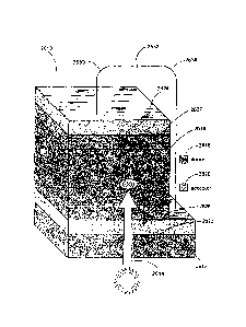
[0048] FIG. 10 is a stylized diagram of a perovskite material device
4400
according to some embodiments. Although various components of the device 4400
are
illustrated as discrete layers comprising contiguous material, it should be
understood that FIG.
is a stylized diagram; thus, embodiments in accordance with it may include
such discrete
layers, and/or substantially intermixed, non-contiguous layers, consistent
with the usage of
"layers" previously discussed herein. The device 4400 includes first and
second substrates
4401 and 4407. A first electrode (ITO) 4402 is disposed upon an inner surface
of the first
substrate 4401, and a second electrode (Ag) 4406 is disposed on an inner
surface of the second
substrate 4407. An active layer 4450 is sandwiched between the two electrodes
4402 and
4406. The active layer 4450 includes a first IFL (e.g., SrTiO3) 4403, a
photoactive material
(e.g., MAPbI3) 4404, and a charge transport layer (e.g., Spiro-OMeTAD) 4405.
[0049] The thin-coat IFLs and methods of coating them onto TiO2
previously
discussed may, in some embodiments, be employed in DSSCs comprising liquid
electrolytes.
Thus, returning to the example of a thin-coat IFL and referring back to FIG. I
for an example,
the DSSC of FIG. 1 could further comprise a thin-coat IFL as described above
coated onto the
mesoporous layer 1505 (that is, the thin-coat IFL would be inserted between
mesoporous layer
1505 and dye 1504).
[0050] In one embodiment, a perovskite material device may be
formulated by
casting Pb12 onto a SrTiO3-coated ITO substrate. The Pb12 may be converted to
MAPb13 by a
dipping process. This process is described in greater detail below. This
conversion process is
more complete (as observed by optical spectroscopy) as compared to the
preparation of the
substrate without SrTiO3.
18
CA 3038358 2019-03-29
[0051] In some embodiments, the thin-coat IFLs previously discussed
in the
context of DSSCs may be used in any interfacial layer of a semiconductor
device such as a PV
(e.g., a hybrid PV or other PV), field-effect transistor, light-emitting
diode, non-linear optical
device, memristor, capacitor, rectifier, rectifying antenna, etc. Furthermore,
thin-coat IFLs of
some embodiments may be employed in any of various devices in combination with
other
compounds discussed in the present disclosure, including but not limited to
any one or more of
the following of various embodiments of the present disclosure: solid hole-
transport material
such as active material and additives (such as, in some embodiments,
chenodeoxycholic acid or
1,8- diiodooctane).
[0052] In some embodiments, multiple IFLs made from different
materials may
be arranged adjacent to each other to form a composite IFL. This configuration
may involve
two different IFLs, three different IFLs, or an even greater number of
different IFLs. The
resulting multi-layer IFL or composite EFL may be used in lieu of a single-
material EFL. For
example, a composite IFL may be used as IFL 2626 and/or as IFL 2627 in cell
2610, shown in
the example of FIG. 4. While the composite IFL differs from a single-material
IFL, the
assembly of a perovskite material PV cell having multi-layer IFLs is not
substantially different
than the assembly of a perovskite material PV cell having only single-material
1FLs.
[0053] Generally, the composite IFL may be made using any of the
materials
discussed herein as suitable for an IFL. In one embodiment, the IFL comprises
a layer of
Al2O3 and a layer of ZnO or M:ZnO (doped ZnO, e.g., Be:ZnO, Mg:ZnO, Ca:ZnO,
Sr:ZnO,
Ba:ZnO, Sc:ZnO, Y:ZnO, Nb:Zn0). In an embodiment, the IFL comprises a layer of
ZrO2 and
a layer of ZnO or M:ZnO. In certain embodiments, the IFL comprises multiple
layers. In
some embodiments, a multi-layer IFL generally has a conductor layer, a
dielectric layer, and a
19
CA 3038358 2019-03-29
semi-conductor layer. In particular embodiments the layers may repeat, for
example, a
conductor layer, a dielectric layer, a semi-conductor layer, a dielectric
layer, and a semi-
conductor layer. Examples of multi- layer IFLs include an IFL having an ITO
layer, an Al2O3
layer, a ZnO layer, and a second A1203 layer; an EF'L having an ITO layer, an
A1203 layer, a
ZnO layer, a second A1203 layer, and a second ZnO layer; an IFL having an ITO
layer, an
A1203 layer, a ZnO layer, a second Al2O3 layer, a second ZnO layer, and a
third A1203 layer;
and EFLs having as many layers as necessary to achieve the desired performance
characteristics. As discussed previously, references to certain stoichiometric
ratios are not
intended to limit the ratios of component elements in 1FL layers according to
various
embodiments.
[0054] Arranging two or more adjacent IFLs as a composite 1FL may
outperform
a single FL in perovskite material PV cells where attributes from each IFL
material may be
leveraged in a single rFL. For example, in the architecture having an ITO
layer, an A1203
layer, and a ZnO layer, where ITO is a conducting electrode, Al2O3 is a
dielectric material and
ZnO is a n-type semiconductor, ZnO acts as an electron acceptor with well
performing electron
transport properties (e.g., mobility). Additionally, A1203 is a physically
robust material that
adheres well to ITO, homogenizes the surface by capping surface defects (e.g.,
charge traps),
and improves device diode characteristics through suppression of dark current.
[0055] FIG. 11 is a stylized diagram of a perovskite material device
4500
according to some embodiments Although various components of the device 4500
are
illustrated as discrete layers comprising contiguous material, it should be
understood that FIG.
11 is a stylized diagram; thus, embodiments in accordance with it may include
such discrete
layers, and/or substantially intermixed, non-contiguous layers, consistent
with the usage of
CA 3038358 2019-03-29
"layers" previously discussed herein. The device 4500 includes first and
second substrates
4501 and 4508. A first electrode (e.g., ITO) 4502 is disposed upon an inner
surface of the first
substrate 4501, and a second electrode (e.g., Ag) 4507 is disposed on an inner
surface of the
second substrate 4508. An active layer 4550 is sandwiched between the two
electrodes 4502
and 4507. The active layer 4550 includes a composite IFL comprising a first
IFL (e.g., A1203)
4503 and a second IFL (e.g., ZnO) 4504, a photoactive material (e.g., MAPbI3)
4505, and a
charge transport layer (e.g., Spiro- OMeTAD) 4506.
[0056] FIGS. 13-20 are stylized diagrams of perovskite material
devices
according to some embodiments. Although various components of the devices are
illustrated
as discrete layers comprising contiguous material, it should be understood
that FIGS. 13-18
are stylized diagrams; thus, embodiments in accordance with them may include
such discrete
layers, and/or substantially intermixed, non-contiguous layers, consistent
with the usage of
"layers" previously discussed herein. The example devices include layers and
materials
described throughout this disclosure. The devices may include a substrate
layer (e.g., glass),
electrode layers (e.g., ITO, Ag), interfacial layers, which may be composite
IFLs (e.g., ZnO,
A1203, Y:ZnO, and/or Nb:Zn0), a photoactive material (e.g. MAPbI3, FAPbI3, 5-
AVA=HC1:
MAPbI3, and/or CHP: MAPbI3), and a charge transport layer (e.g., Spiro-OMeTAD,
PCDTBT,
11.B, TPD, PTB7, F8BT, PPV, MDMO-PPV, MEH-PPV, and/or P3HT).
[0057] FIG. 13 is a stylized diagram of a perovskite material device
6100
according to some embodiments. Although various components of the device 6100
are
illustrated as discrete layers comprising contiguous material, it should be
understood that FIG.
13 is a stylized diagram; thus, embodiments in accordance with it may include
such discrete
layers, and/or substantially intermixed, non-contiguous layers, consistent
with the usage of
21
CA 3038358 2019-03-29
"layers" previously discussed herein. The device 6100 includes a substrate
(e.g., Glass) 6101.
A first electrode (e.g., ITO) 6102 is disposed upon an inner surface of the
substrate 6101, and a
second electrode (e.g., Ag) 6107 is disposed on top of an active layer 6150
that is sandwiched
between the two electrodes 6102 and 6107. The active layer 6150 includes a
composite IFL
comprising a first IFL (e.g., A1203) 6103 and a second IFL (e.g., ZnO) 6104, a
photoactive
material (e.g., MAPbI3) 6105, and a charge transport layer (e.g., Spiro-
OMeTAD) 6106.
[0058] FIG. 14 is a stylized diagram of a perovskite material device
6200
according to some embodiments. Although various components of the device 6200
are
illustrated as discrete layers comprising contiguous material, it should be
understood that FIG.
14 is a stylized diagram; thus, embodiments in accordance with it may include
such discrete
layers, and/or substantially intermixed, non-contiguous layers, consistent
with the usage of
"layers" previously discussed herein. The device 6200 includes a substrate
(e.g., Glass) 6201.
A first electrode (e.g., ITO) 6202 is disposed upon an inner surface of the
substrate 6201, and a
second electrode (e.g., Ag) 6206 is disposed on top of an active layer 6250
that is sandwiched
between the two electrodes 6202 and 6206. The active layer 6250 includes an
IFL (e.g.,
Y:ZnO) 6203, a photoactive material (e.g., MAPbI3) 6204, and a charge
transport layer (e.g.,
P3HT) 6205.
[0059] FIG. 15 is a stylized diagram of a perovskite material device
6300
according to some embodiments. Although various components of the device 6300
are
illustrated as discrete layers comprising contiguous material, it should be
understood that FIG.
15 is a stylized diagram; thus, embodiments in accordance with it may include
such discrete
layers, and/or substantially intermixed, non-contiguous layers, consistent
with the usage of
"layers" previously discussed herein. The device 6300 includes a substrate
(e.g., Glass) 6301.
22
CA 3038358 2019-03-29
A first electrode (e.g., ITO) 6302 is disposed upon an inner surface of the
substrate 6301, and a
second electrode (e.g.. Ag) 6309 is disposed on top of an active layer 6350
that is sandwiched
between the two electrodes 6302 and 6309. The active layer 6350 includes a
composite IFL
comprising a first IFL (e.g., A1203) 6303, a second EFL (e.g., ZnO) 6304, a
third IFL (e.g.,
A1203) 6305, and a fourth IFL (e.g., ZnO) 6306, a photoactive material (e.g.,
MAPb13) 6307,
and a charge transport layer (e.g., PCDTBT) 6308.
[0060] FIG. 16 is a stylized diagram of a perovskite material device
6400
according to some embodiments. Although various components of the device 6400
are
illustrated as discrete layers comprising contiguous material, it should be
understood that FIG.
16 is a stylized diagram; thus, embodiments in accordance with it may include
such discrete
layers, and/or substantially intermixed, non-contiguous layers, consistent
with the usage of
"layers" previously discussed herein. The device 6400 includes a substrate
(e.g., Glass) 6401.
A first electrode (e.g., ITO) 6402 is disposed upon an inner surface of the
substrate 6401, and a
second electrode (e.g., Ag) 6409 is disposed on top of an active layer 6450
that is sandwiched
between the two electrodes 6402 and 6409. The active layer 6450 includes a
composite EL
comprising a first IFL (e.g., A1203) 6403, a second IFL (e.g., ZnO) 6404, a
third IFL (e.g.,
A1203) 6405, and a fourth IFL (e.g., ZnO) 6406, a photoactive material (e.g.,
5-AVA-
HaMAPb13) 6407, and a charge transport layer (e.g., PCDTBT) 6408.
[0061] FIG. 17 is a stylized diagram of a perovskite material device
6500
according to some embodiments. Although various components of the device 6500
are
illustrated as discrete layers comprising contiguous material, it should be
understood that FIG.
17 is a stylized diagram; thus, embodiments in accordance with it may include
such discrete
layers, and/or substantially intermixed, non-contiguous layers, consistent
with the usage of
23
CA 3038358 2019-03-29
"layers" previously discussed herein. The device 6500 includes a substrate
(e.g., Glass) 6501.
A first electrode (e.g., ITO) 6502 is disposed upon an inner surface of the
substrate 6501, and a
second electrode (e.g., Ag) 6506 is disposed on top of an active layer 6550
that is sandwiched
between the two electrodes 6502 and 6506. The active layer 6550 includes an
IFL (e.g.,
Nb:ZnO) 6503, a photoactive material (e.g., FAPb13) 6504, and a charge
transport layer (e.g.,
P3HT) 6505.
[0062] FIG. 18 is a stylized diagram of a perovskite material device
6600
according to some embodiments. Although various components of the device 6600
are
illustrated as discrete layers comprising contiguous material, it should be
understood that FIG.
18 is a stylized diagram; thus, embodiments in accordance with it may include
such discrete
layers, and/or substantially intermixed, non-contiguous layers, consistent
with the usage of
"layers" previously discussed herein. The device 6600 includes a substrate
(e.g., Glass) 6601.
A first electrode (e.g., ITO) 6602 is disposed upon an inner surface of the
substrate 6601, and a
second electrode (e.g., Ag) 6606 is disposed on top of an active layer 6650
that is sandwiched
between the two electrodes 6602 and 6606. The active layer 6650 includes an
IFL (e.g.,
Y:ZnO) 6603, a photoactive material (e.g., CHP;MAPbI3) 6604, and a charge
transport layer
(e.g., P3 HT) 6605.
[0063] FIG. 19 is a stylized diagram of a perovskite material device
6700
according to some embodiments. Although various components of the device 6700
are
illustrated as discrete layers comprising contiguous material, it should be
understood that FIG.
19 is a stylized diagram; thus, embodiments in accordance with it may include
such discrete
layers, and/or substantially intermixed, non-contiguous layers, consistent
with the usage of
"layers" previously discussed herein. The device 6700 includes a substrate
(e.g., Glass) 6701.
24
CA 3038358 2019-03-29
A first electrode (e.g., ITO) 6702 is disposed upon an inner surface of the
substrate 6701, and a
second electrode (e.g., Al) 6707 is disposed on top of an active layer 6750
that is sandwiched
between the two electrodes 6702 and 6707. The active layer 6750 includes an
IFL (e.g.,
SrTiO3) 6703 a photoactive material (e.g., FAPbI3) 6704, a first charge
transport layer (e.g.,
P3HT) 6705, and a second charge transport layer (e.g., Mo0x) 6706.
[0064] FIG. 20 is a stylized diagram of a perovskite material device
6800
according to some embodiments. Although various components of the device 6800
are
illustrated as discrete layers comprising contiguous material, it should be
understood that FIG.
16 is a stylized diagram; thus, embodiments in accordance with it may include
such discrete
layers, and/or substantially intermixed, non-contiguous layers, consistent
with the usage of
"layers" previously discussed herein. The device 6800 includes a substrate
(e.g., Glass) 6801.
A first electrode (e.g., ITO) 6802 is disposed upon an inner surface of the
substrate 6801, and a
second electrode (e.g., Al) 6811 is disposed on top of an active layer 6850
that is sandwiched
between the two electrodes 6802 and 6811. The active layer 6850 includes a
composite IFL
comprising a first IFL (e.g., A1203) 6803, a second IFL (e.g., ZnO) 6804, a
third IFL (e.g.,
A1203) 6805, a fourth IFL (e.g., ZnO) 6806, and a fifth IFL (e.g., Al2O3)
6807, a photoactive
material (e.g., FAPbI3) 6808, a first charge transport layer (e.g., P3HT)
6809, and a second
charge transport layer (e.g., Mo0x) 6810.
[0065] Perovskite Material
[0066] A perovskite material may be incorporated into one or more
aspects of a
PV or other device. A perovskite material according to some embodiments may be
of the
general formula CMX3, where: C comprises one or more cations (e.g., an amine,
ammonium, a
Group I metal, a Group 2 metal, and/or other cations or cation-like
compounds); M comprises
?.5
CA 3038358 2019-03-29
one or more metals (examples including Fe, Co, Ni, Cu, Sn, Pb, Bi, Ge, Ti, and
Zr); and X
comprises one or more anions. In some embodiments, C may include one or more
organic
cations.
[0067] In certain
embodiments, C may include an ammonium, an organic cation
of the general formula [NR4]+ where the R groups may be the same or different
groups.
Suitable R groups include, but are not limited to: methyl, ethyl, propyl,
butyl, pentyl group or
isomer thereof; any alkane, alkene, or alkyne CxHy, where x 1 - 20, y = 1 -
42, cyclic,
branched or straight-chain; alkyl halides, CxflyXz, x = I - 20, y = 0 - 42, z
= 1 - 42, X = F, Cl,
Br, or I; any aromatic group (e.g., phenyl, alkylphenl, alkoxyphenyl,
pyridine, naphthalene);
cyclic complexes where at least one nitrogen is contained within the ring
(e.g., pyridine,
pyrrole, pyrrolidine, piperidine, tetrahydroquinoline); any sulfur-containing
group (e.g.,
sulfoxide, thiol, alkyl sulfide); any nitrogen-containing group (nitroxide,
amine); any
phosphorous containing group (phosphate); any boron-containing group (e.g.,
boronic acid);
any organic acid (e.g., acetic acid, propanoic acid); and ester or amide
derivatives thereof; any
amino acid (e.g., glycine, cysteine, proline, glutamic acid, arginine, serine,
histindine, 5-
ammoniumvaleric acid) including alpha, beta, gamma, and greater derivatives;
any silicon
containing group (e.g., siloxane); and any alkoxy or group, -0CxHy, where x =
0 - 20, y = 1 -
42.
[0068] In certain
embodiments, C may include a formamidinium, an organic
cation of the general formula [12.7NCRNR2I where the R groups may be the same
or different
groups. Suitable R groups include, but are not limited to. hydrogen, methyl,
ethyl, propyl,
butyl, pentyl group or isomer thereof; any alkane, alkene, or alkyne CxHy,
where x = 1 - 20, y
= 1 - 42, cyclic, branched or straight-chain; alkyl halides, CxflyXz, x = I -
20, y 0 - 42, z = 1
26
CA 3038358 2019-03-29
..
..
- 42, X = F, Cl, Br, or 1; any aromatic group (e.g., phenyl, alkylphenl,
alkoxyphenyl, pyridine,
naphthalene); cyclic complexes where at least one nitrogen is contained within
the ring (e.g.,
imidazole, benzimidazole, di hydropyri mi di ne, (azoli di nyl i denem
ethyl)pyrrol i di ne, triazole);
any sulfur- containing group (e.g., sulfoxide, thiol, alkyl sulfide); any
nitrogen-containing
group (nitroxide, amine); any phosphorous containing group (phosphate); any
boron-
containing group (e.g., boronic acid); any organic acid (acetic acid,
propanoic acid) and ester
or amide derivatives thereof; any amino acid (e.g., glycine, cysteine,
proline, glutamic acid,
arginine, serine, histindine, 5-ammoniumvaleric acid) including alpha, beta,
gamma, and
greater derivatives; any silicon containing group (e.g., siloxane); and any
alkoxy or group, -
0CxHy, where x = 0 - 20, y = 1 -42.
R5
ve,L4 RI R3
"%=-. 'I
IL L
Formula 1
[0069] Formula 1 illustrates the structure of a formamidinium
cation having the
general formula of [R2NCRNR2]+ as described above. Formula 2 illustrates
examples
structures of several formamidinium cations that may serve as a cation "C" in
a perovskite
material.
27
CA 3038358 2019-03-29
rrN,
kiiNowt.lkm~ssogobta
00.14e2ItirorgiyimeissmOursemkri
Formula 2
[0070] In certain
embodiments, C may include a guanidinium, an organic cation
of the general formula [(R2N)2C=NR21# where the R groups may be the same or
different
groups. Suitable R groups include, but are not limited to: hydrogen, methyl,
ethyl, propyl,
butyl, pentyl group or isomer thereof; any alkane, alkene, or alkyne CxHy,
where x = 1 - 20, y
= 1 - 42, cyclic, branched or straight-chain; alkyl halides, CxFlyXz, x = 1 -
20, y = 0 -42, z = 1
- 42, X = F, Cl, Br, or I; any aromatic group (e.g., phenyl, alkylphenl,
alkoxyphenyl, pyridine,
naphthalene); cyclic complexes where at least one nitrogen is contained within
the ring (e.g.,
octahydropyrimido[ I,2-a]pyrimidine, pyrimido [1,2-a]pyrimidine,
hexahydroimidazo [1,2-
alimidazole, hexahydropyrimidin-2-imine ); any sulfur-containing group (e.g.,
sulfoxide, thiol,
28
CA 3038358 2019-03-29
alkyl sulfide); any nitrogen-containing group (nitroxide, amine); any
phosphorous containing
group (phosphate); any boron-containing group (e.g., boronic acid); any
organic acid (acetic
acid, propanoic acid) and ester or amide derivatives thereof; any amino acid
(e.g., glycine,
cysteine, proline, glutamic acid, arginine, serine, histindine, 5-
ammoniumvaleric acid)
including alpha, beta, gamma, and greater derivatives; any silicon containing
group (e.g.,
siloxane); and any alkoxy or group, -0CxHy, where x = 0 - 20, y = 1 - 42.
Rt,JR3
N1/4ti
Formula 3
[0071] Formula 3
illustrates the structure of a guanidinium cation having the
general formula of [(R2N)2C=NR2]+ as described above. Formula 4 illustrates
examples of
structures of
several guanidinium cations that may serve as a cation "C" in a perovskite
material.
29
CA 3038358 2019-03-29
=
..
-
NS=.-i,"LN. ""
lArttalagtiteybartirtfigrkkilelilkintamzvo
.i. ..1 t
' N.,. ,..p= -
1Aniv-Malmwtkiatineotusivla+ttRAnnaiktieravti.oin
CO-
i,i4.-"L
Z151:roatrOm-t14-n;ivoli NorMILAIth7 ass
i Ni12
*44e:::-S4N,L .
EXT.,:r*i;wk./ApavirtoppaiNtoiiPpcfrAtahytionc,reda
...õ:( !. \
. '.....
µs\...õ....õ...iks....
N . =
g3.a.F..,=:24iam.lerde:Oweliv4ill4ttioggoramitea
iftinniartairvalmottrrissrolOsimParimsrks^is
WI C31A.
tP=
...,,,Lt, 0, I
...,õ
,A:r.....,.......,,,,ri......2õ..,_:4.:,,...........:
Formula 4
CA 3038358 2019-03-29
[0072] In certain
embodiments, C may include an ethene tetramine cation, an
organic cation of the general formula [(R2N)2C=C(NR2)21+ where the R groups
may be the
same or different groups. Suitable R groups include, but are not limited to:
hydrogen, methyl,
ethyl, propyl, butyl, pentyl group or isomer thereof; any alkane, alkene, or
alkyne CxHy, where
x = 1 - 20, y = 1 - 42, cyclic, branched or straight-chain; alkyl halides,
CxHyXz, x = 1 - 20, y --
0 - 42, z I - 42, X = F,
Cl, Br, or I; any aromatic group (e.g., phenyl, alkylphenl,
alkoxyphenyl, pyridine, naphthalene); cyclic complexes where at least one
nitrogen is
contained within the ring (e.g., 2-hexahydropyrimidin-2-
ylidenehexahydropyrimidine,
octahydropyrazino [2,3-b]pyrazine, pyrazino[2,3-b ]pyrazine, quinoxalino[2,3-b
]quinoxaline);
any sulfur-containing group (e.g., sulfoxide, thiol, alkyl sulfide); any
nitrogen-containing group
(nitroxide, amine); any phosphorous containing group (phosphate); any boron-
containing
group (e.g., boronic acid); any organic acid (acetic acid, propanoic acid) and
ester or amide
derivatives thereof; any amino acid (e.g., glycine, cysteine, proline,
glutamic acid, arginine,
serine, histindine, 5-ammoniumvaleric acid) including alpha, beta, gamma, and
greater
derivatives; any silicon containing group (e.g., siloxane); and any alkoxy or
group, -0CxHy,
where x = 0 - 20, y = 1 - 42.
R. R3
Ft 1Ø*==1 R4
Ro-N RS
\7 RI
Formula 5
[0073] Formula 5
illustrates the structure of an ethene tetramine cation having the
general formula of [(R2N)2C=C(NR2)2]+ as described above. Formula 6
illustrates examples of
31
CA 3038358 2019-03-29
structures of several ethene tetramine ions that may serve as a cation "C" in
a perovskite
material.
2-hexahydropyrimidin-2-ylidenehexahydropyrimidne
ier---XD
..,
pyrazino[2,3-b]pyraztine
Cal ?µ)
N
1,2,3,4,5,6,7,8-octahydropyrazino[2, 3-b]pyrazine
N t
N =
quinoxalino[2, 3-b]quinoxaline
Formula 6
[0074] In certain embodiments, C may include an imidazolium cation,
an
aromatic, cyclic organic cation of the general formula [CRNRCRNRCR]+ where the
R groups
may be the same or different groups. Suitable R groups may include, but are
not limited to:
hydrogen, methyl, ethyl, propyl, butyl, pentyl group or isomer thereof; any
alkane, alkene, or
alkyne CxHy, where x = 1 - 20, y = 1 - 42, cyclic, branched or straight-chain;
alkyl halides,
CxHyXz, x = 1 - 20, y = 0 -42, z = 1 -42, X = F, Cl, Br, or I; any aromatic
group (e.g., phenyl,
alkylphenl, alkoxyphenyl, pyridine, naphthalene); cyclic complexes where at
least one nitrogen
is contained within the ring (e.g., 2-hexahydropyrimidin-2-
ylidenehexahydropyrimidine,
octahydropyrazino[2,3-b ]pyrazine, pyrazino[2,3-b ]pyrazine, quinoxalino[2,3-b
lquinoxaline);
32
CA 3038358 2019-03-29
any sulfur-containing group (e.g., sulfoxide, thiol, alkyl sulfide); any
nitrogen-containing group
(nitroxide, amine); any phosphorous containing group (phosphate); any boron-
containing
group (e.g., boronic acid); any organic acid (acetic acid, propanoic acid) and
ester or amide
derivatives thereof; any amino acid (e.g., glycine, cysteine, proline,
glutamic acid, arginine,
serine, histindine, 5-ammoniumvaleric acid) including alpha, beta, gamma, and
greater
derivatives; any silicon containing group (e.g., siloxane); and any alkoxy or
group, -0CxHy,
where x = 0 - 20, y = 1 -42.
000.00L R
.005
Formula 7
[0075] In some
embodiments, X may include one or more halides. In certain
embodiments, X may instead or in addition include a Group 16 anion. In certain
embodiments,
the Group 16 anion may be sulfide or selenide. In certain embodiments, X may
instead or in
addition include one or more a pseudohalides (e.g., cyanide, cyanate,
isocyanate, fulminate,
thiocyanate, i sot hi ocyanate, azi de, tetracarbonyl cobal tate, carbam oyl
di cyan om ethani de,
dicyanonitrosomethanide, dicyanamide, and tricyanomethanide ). In some
embodiments, each
organic cation C may be larger than each metal M, and each anion X may be
capable of
bonding with both a cation C and a metal M. Examples of perovskite materials
according to
various embodiments include CsSnI3 (previously discussed herein) and Cs,Sn,I2
(with x, y, and
33
CA 3038358 2019-03-29
z varying in accordance with the previous discussion). Other examples include
compounds of
the general formula CsSnX3, where X may be any one or more of: 13, 12.9sFo os;
120; IC12; and
C13. In other embodiments, X may comprise any one or more of 1, Cl, F, and Br
in amounts
such that the total ratio of X as compared to Cs and Sn results in the general
stoichiometry of
CsSnX3. In some embodiments, the combined stoichiometry of the elements that
constitute X
may follow the same rules as I, as previously discussed with respect to
CsSnyI,. Yet other
examples include compounds of the general formula RNH3PbX3, where R may be C.1-
1211+1,
with n ranging from 0-10, and X may include any one or more of F, Cl, Br, and
I in amounts
such that the total ratio of X as compared to the cation RNH3 and metal Pb
results in the
general stoichiometry of RNH3PbX3. Further, some specific examples of R
include H, alkyl
chains (e.g., CH3, CH3CH2, CH3CH2CH2, and so on), and amino acids (e.g.,
glycine, cysteine,
proline, glutamic acid, arginine, serine, histindine, 5-ammoniumvaleric acid)
including alpha,
beta, gamma, and greater derivatives.
[0076] Composite Perovskite Material Device Design
[0077] In some embodiments, the present disclosure may provide
composite
design of PV and other similar devices (e.g., batteries, hybrid PV batteries,
FETs, LEDs,
nonlinear optics (NLOs), waveguides, etc.) including one or more perovskite
materials. For
example, one or more perovskite materials may serve as either or both of first
and second
active material of some embodiments (e.g., active materials 2810 and 2815 of
FIG. 5). In more
general terms, some embodiments of the present disclosure provide PV or other
devices having
an active layer comprising one or more perovskite materials. In such
embodiments, perovskite
material (that is, material including any one or more perovskite materials(s))
may be employed
in active layers of various architectures. Furthermore, perovskite material
may serve the
34
CA 3038358 2019-03-29
function(s) of any one or more components of an active layer (e.g., charge
transport material,
mesoporous material, photoactive material, and/or interfacial material, each
of which is
discussed in greater detail below). In some embodiments, the same perovskite
materials may
serve multiple such functions, although in other embodiments, a plurality of
perovskite
materials may be included in a device, each perovskite material serving one or
more such
functions. In certain embodiments, whatever role a perovskite material may
serve, it may be
prepared and/or present in a device in various states. For example, it may be
substantially solid
in some embodiments. In other embodiments, it may be a solution (e.g.,
perovskite material
may be dissolved in liquid and present in said liquid in its individual ionic
subspecies); or it
may be a suspension (e.g., of perovskite material particles). A solution or
suspension may be
coated or otherwise deposited within a device (e.g., on another component of
the device such
as a mesoporous, interfacial, charge transport, photoactive, or other layer,
and/or on an
electrode). Perovskite materials in some embodiments may be formed in situ on
a surface of
another component of a device (e.g., by vapor deposition as a thin-film
solid). Any other
suitable means of forming a solid or liquid layer comprising perovskite
material may be
employed.
[0078] In general, a
perovskite material device may include a first electrode, a
second electrode, and an active layer comprising a perovskite material, the
active layer
disposed at least partially between the first and second electrodes In some
embodiments, the
first electrode may be one of an anode and a cathode, and the second electrode
may be the
other of an anode and cathode. An active layer according to certain
embodiments may include
any one or more active layer components, including any one or more of: charge
transport
material; liquid electrolyte; mesoporous material; photoactive material (e.g.,
a dye, silicon,
CA 3038358 2019-03-29
cadmium telluride, cadmium sulfide, cadmium selenide, copper indium gallium
selenide,
gallium arsenide, germanium indium phosphide, semiconducting polymers, other
photoactive
materials)); and interfacial material. Any one or more of these active layer
components may
include one or more perovskite materials. In some embodiments, some or all of
the active
layer components may be in whole or in part arranged in sub-layers. For
example, the active
layer may comprise any one or more of: an interfacial layer including
interfacial material; a
mesoporous layer including mesoporous material; and a charge transport layer
including
charge transport material. In some embodiments, photoactive material such as a
dye may be
coated on, or otherwise disposed on, any one or more of these layers. In
certain embodiments,
any one or more layers may be coated with a liquid electrolyte. Further, an
interfacial layer
may be included between any two or more other layers of an active layer
according to some
embodiments, and/or between a layer and a coating (such as between a dye and a
mesoporous
layer), and/or between two coatings (such as between a liquid electrolyte and
a dye), and/or
between an active layer component and an electrode. Reference to layers herein
may include
either a final arrangement (e.g., substantially discrete portions of each
material separately
definable within the device), and/or reference to a layer may mean arrangement
during
construction of a device, notwithstanding the possibility of subsequent
intermixing of
material(s) in each layer. Layers may in some embodiments be discrete and
comprise
substantially contiguous material (e.g., layers may be as stylistically
illustrated in FIG. 1). In
other embodiments, layers may be substantially intermixed (as in the case of,
e.g., BM, hybrid,
and some DSSC cells), an example of which is shown by first and second active
material 2618
and 2620 within photoactive layer 2616 in FIG 4. In some embodiments, a device
may
comprise a mixture of these two kinds of layers, as is also shown by the
device of FIG. 4,
36
CA 3038358 2019-03-29
which contains discrete contiguous layers 2627, 2626, and 2622, in addition to
a photoactive
layer 2616 comprising intermixed layers of first and second active material
2618 and 2620. In
any case, any two or more layers of whatever kind may in certain embodiments
be disposed
adjacent to each other (and/or intermixedly with each other) in such a way as
to achieve a high
contact surface area. In certain embodiments, a layer comprising perovskite
material may be
disposed adjacent to one or more other layers so as to achieve high contact
surface area (e.g.,
where a perovskite material exhibits low charge mobility). In other
embodiments, high contact
surface area may not be necessary (e.g., where a perovskite material exhibits
high charge
mobility).
[0079] A perovskite material device according to some embodiments may
optionally include one or more substrates. In some embodiments, either or both
of the first and
second electrode may be coated or otherwise disposed upon a substrate, such
that the electrode
is disposed substantially between a substrate and the active layer. The
materials of
composition of devices (e.g., substrate, electrode, active layer and/or active
layer components)
may in whole or in part be either rigid or flexible in various embodiments. In
some
embodiments, an electrode may act as a substrate, thereby negating the need
for a separate
substrate.
[0080] Furthermore, a perovskite material device according to certain
embodiments may optionally include light-harvesting material (e.g., in a light-
harvesting layer,
such as Light Harvesting Layer 1601 as depicted in the example PV represented
in FIG. 2). In
addition, a perovskite material device may include any one or more additives,
such as any one
or more of the additives discussed above with respect to some embodiments of
the present
disclosure.
37
CA 3038358 2019-03-29
[0081] Description of
some of the various materials that may be included in a
perovskite material device will be made in part with reference to FIG. 7. FIG.
7 is a stylized
diagram of a perovskite material device 3900 according to some embodiments.
Although
various components of the device 3900 are illustrated as discrete layers
comprising contiguous
material, it should be understood that FIG. 7 is a stylized diagram; thus,
embodiments in
accordance with it may include such discrete layers, and/or substantially
intermixed, non-
contiguous layers, consistent with the usage of "layers" previously discussed
herein. The
device 3900 includes first and second substrates 3901 and 3913. A first
electrode 3902 is
disposed upon an inner surface of the first substrate 3901, and a second
electrode 3912 is
disposed on an inner surface of the second substrate 3913. An active layer
3950 is sandwiched
between the two electrodes 3902 and 3912. The active layer 3950 includes a
mesoporous layer
3904; first and second photoactive materials 3906 and 3908; a charge transport
layer 3910, and
several interfacial layers. FIG. 7 furthermore illustrates an example device
3900 according to
embodiments wherein sub-layers of the active layer 3950 are separated by the
interfacial
layers, and further wherein interfacial layers are disposed upon each
electrode 3902 and 3912.
In particular, second, third, and fourth interfacial layers 3905, 3907, and
3909 are respectively
disposed between each of the mesoporous layer 3904, first photoactive material
3906, second
photoactive material 3908, and charge transport layer 3910. First and fifth
interfacial layers
3903 and 3911 are respectively disposed between (i) the first electrode 3902
and mesoporous
layer 3904; and (ii) the charge transport layer 3910 and second electrode
3912. Thus, the
architecture of the example device depicted in FIG. 7 may be characterized as:
substrate-
electrode-active layer-electrode-substrate. The architecture of the active
layer 3950 may be
characterized as: interfacial layer-mesoporous I ayer-i nterfaci al I ayer-
photoactive m ateri al -
38
CA 3038358 2019-03-29
interfacial layer-photoactive mated al -interfaci al layer-charge transport
layer-interfaci al layer.
As noted previously, in some embodiments, interfacial layers need not be
present; or, one or
more interfacial layers may be included only between certain, but not all,
components of an
active layer and/or components of a device.
[0082] A substrate, such as either or both of first and second
substrates 3901 and
3913, may be flexible or rigid. If two substrates are included, at least one
should be
transparent or translucent to electromagnetic (EM) radiation (such as, e.g.,
UV, visible, or IR
radiation). If one substrate is included, it may be similarly transparent or
translucent, although
it need not be, so long as a portion of the device permits EM radiation to
contact the active
layer 3950. Suitable substrate materials include any one or more of: glass;
sapphire;
magnesium oxide (MgO); mica; polymers (e.g., PET, PEG, polypropylene,
polyethylene, etc.);
ceramics; fabrics (e.g., cotton, silk, wool); wood; drywall; metal; and
combinations thereof.
[0083] As previously noted, an electrode (e.g., one of electrodes
3902 and 3912
of FIG. 7) may be either an anode or a cathode. In some embodiments, one
electrode may
function as a cathode, and the other may function as an anode. Either or both
electrodes 3902
and 3912 may be coupled to leads, cables, wires, or other means enabling
charge transport to
and/or from the device 3900. An electrode may constitute any conductive
material, and at least
one electrode should be transparent or translucent to EM radiation, and/or be
arranged in a
manner that allows EM radiation to contact at least a portion of the active
layer 3950. Suitable
electrode materials may include any one or more of: indium tin oxide or tin-
doped indium
oxide (ITO); fluorine- doped tin oxide (FT0); cadmium oxide (CdO); zinc indium
tin oxide
(ZITO); aluminum zinc oxide (A70); aluminum (Al); gold (Au); calcium (Ca);
magnesium
(Mg); titanium (Ti); steel, carbon (and allotropes thereof), and combinations
thereof.
39
CA 3038358 2019-03-29
[0084] ivlesoporous
material (e.g., the material included in mesoporous layer
3904 of FIG. 7) may include any pore-containing material. In some embodiments,
the pores
may have diameters ranging from about 1 to about 100 nm; in other embodiments,
pore
diameter may range from about 2 to about 50 nm. Suitable mesoporous material
includes any
one or more of: any interfacial material and/or mesoporous material discussed
elsewhere
herein; aluminum (Al); bismuth (Bi); indium (In); molybdenum (Mo); niobium
(Nb); nickel
(Ni); silicon (Si); titanium (Ti); vanadium (V); zinc (Zn); zirconium (Zr); an
oxide of any one
or more of the foregoing metals (e.g., alumina, ceria, titania, zinc oxide,
zircona, etc.); a sulfide
of any one or more of the foregoing metals; a nitride of any one or more of
the foregoing
metals; and combinations thereof.
[0085] Photoactive
material (e.g., first or second photoactive material 3906 or
3908 of FIG. 7) may comprise any photoactive compound, such as any one or more
of silicon
(in some instances, single-crystalline silicon), cadmium telluride, cadmium
sulfide, cadmium
selenide, copper indium gallium selenide, gallium arsenide, germanium indium
phosphide, one
or more semiconducting polymers, and combinations thereof. In certain
embodiments,
photoactive material may instead or in addition comprise a dye (e.g., N719,
N3, other
ruthenium-based dyes). In some embodiments, a dye (of whatever composition)
may be coated
onto another layer (e.g., a mesoporous layer and/or an interfacial layer)
In some
embodiments, photoactive material may include one or more perovskite
materials. Perovskite-
material-containing photoactive substance may be of a solid form, or in some
embodiments it
may take the form of a dye that includes a suspension or solution comprising
perovskite
material. Such a solution or suspension may be coated onto other device
components in a
manner similar to other dyes. In some embodiments, solid perovskite-containing
material may
CA 3038358 2019-03-29
be deposited by any suitable means (e.g., vapor deposition, solution
deposition, direct
placement of solid material, etc.). Devices according to various embodiments
may include
one, two, three, or more photoactive compounds (e.g., one, two, three, or more
perovskite
materials, dyes, or combinations thereof). In certain embodiments including
multiple dyes or
other photoactive materials, each of the two or more dyes or other photoactive
materials may
be separated by one or more interfacial layers. In some embodiments, multiple
dyes and/or
photoactive compounds may be at least in part intermixed.
[0086] Charge
transport material (e.g., charge transport material of charge
transport layer 3910 in FIG. 7) may include solid-state charge transport
material (i.e., a
colloquially labeled solid-state electrolyte), or it may include a liquid
electrolyte and/or ionic
liquid. Any of the liquid electrolyte, ionic liquid, and solid-state charge
transport material may
be referred to as charge transport material. As used herein, "charge transport
material" refers
to any material, solid, liquid, or otherwise, capable of collecting charge
carriers and/or
transporting charge carriers. For instance, in PV devices according to some
embodiments, a
charge transport material may be capable of transporting charge carriers to an
electrode.
Charge carriers may include holes (the transport of which could make the
charge transport
material just as properly labeled "hole transport material") and electrons.
Holes may be
transported toward an anode, and electrons toward a cathode, depending upon
placement of the
charge transport material in relation to either a cathode or anode in a PV or
other device.
Suitable examples of charge transport material according to some embodiments
may include
any one or more of: perovskite material; I713'; Co complexes; polythiophenes
(e.g., poly(3-
hexylthiophene) and derivatives thereof, or P3HT); carbazole-based copolymers
such as
polyheptadecanylcarbazole dithienylbenzothiadiazole and derivatives thereof
(e.g., PCDTBT),
41
CA 3038358 2019-03-29
other copolymers such as polycyclopentadithiophene-benzothiadiazole and
derivatives thereof
(e.g., PCPDTBT), polybenzodithiophenyl-thienothiophenediyl and derivatives
thereof (e g.,
PTB6, PTB7, PTB7-th, PCE-10); poly(triaryl amine) compounds and derivatives
thereof (e.g.,
PTAA); Spiro-OMeTAD; polyphenylene vinylenes and derivatives thereof (e.g,
MDMO-PPV,
MEH-PPV); fullerenes and/or fullerene derivatives (e.g., C60, PCB1v1); and
combinations
thereof. In certain embodiments, charge transport material may include any
material, solid or
liquid, capable of collecting charge carriers (electrons or holes), and/or
capable of transporting
charge carriers. Charge transport material of some embodiments therefore may
be N- or P-type
active and/or semi-conducting material. Charge transport material may be
disposed proximate
to one of the electrodes of a device. It may in some embodiments be disposed
adjacent to an
electrode, although in other embodiments an interfacial layer may be disposed
between the
charge transport material and an electrode (as shown, e.g., in FIG. 7 with the
fifth interfacial
layer 3911). In certain embodiments, the type of charge transport material may
be selected
based upon the electrode to which it is proximate. For example, if the charge
transport
material collects and/or transports holes, it may be proximate to an anode so
as to transport
holes to the anode. However, the charge transport material may instead be
placed proximate to
a cathode, and be selected or constructed so as to transport electrons to the
cathode.
[0087] As previously
noted, devices according to various embodiments may
optionally include an interfacial layer between any two other layers and/or
materials, although
devices according to some embodiments need not contain any interfacial layers.
Thus, for
example, a perovskite material device may contain zero, one, two, three, four,
five, or more
interfacial layers (such as the example device of FIG. 7, which contains five
interfacial layers
3903, 3905, 3907, 3909, and 3911). An interfacial layer may include a thin-
coat interfacial
42
CA 3038358 2019-03-29
layer in accordance with embodiments previously discussed herein (e g.,
comprising alumina
and/or other metal- oxide particles, and/or a titania/metal-oxide bilayer,
and/or other
compounds in accordance with thin-coat interfacial layers as discussed
elsewhere herein). An
interfacial layer according to some embodiments may include any suitable
material for
enhancing charge transport and/or collection between two layers or materials;
it may also help
prevent or reduce the likelihood of charge recombination once a charge has
been transported
away from one of the materials adjacent to the interfacial layer. Suitable
interfacial materials
may include any one or more of: any mesoporous material and/or interfacial
material discussed
elsewhere herein; Al; Bi; Co; Cu; Fe; In; Mn; Mo; Ni; platinum (Pt); Si; Sn;
Ta; Ti; V; W; Nb;
Zn; Zr; oxides of any of the foregoing metals (e.g., alumina, silica,
titania); a sulfide of any of
the foregoing metals; a nitride of any of the foregoing metals; functionalized
or non-
functionalized alkyl silyl groups; graphite; gaphene; fullerenes; carbon
nanotubes; and
combinations thereof (including, in some embodiments, bilayers of combined
materials). In
some embodiments, an interfacial layer may include perovskite material.
[0088] A device
according to the stylized representation of FIG. 7 may in some
embodiments be a PV, such as a DSSC, BH.J, or hybrid solar cell. In some
embodiments,
devices according to FIG. 7 may constitute parallel or serial multi-cell PVs,
batteries, hybrid
PV batteries, FETs, LEDS, and/or any other device discussed herein. For
example, a BHJ of
some embodiments may include two electrodes corresponding to electrodes 3902
and 3912,
and an active layer comprising at least two materials in a heterojunction
interface (e.g., any two
of the materials and/or layers of active layer 3950). In certain embodiments,
other devices
(such as hybrid PV batteries, parallel or serial multi-cell PVs, etc.) may
comprise an active
layer including a perovskite material, corresponding to active layer 3950 of
FIG. 7 In short,
43
CA 3038358 2019-03-29
the stylized nature of the depiction of the example device of FIG. 7 should in
no way limit the
permissible structure or architecture of devices of various embodiments in
accordance with
FIG. 7.
[0089] Additional, more specific, example embodiments of perovskite
devices
will be discussed in terms of further stylized depictions of example devices.
The stylized
nature of these depictions, FIGs. 8-18, similarly is not intended to restrict
the type of device
which may in some embodiments be constructed in accordance with any one or
more of FIGs.
8-18. That is, the architectures exhibited in FIGs. 8-18 may be adapted so as
to provide the
BHJs, batteries, FETs, hybrid PV batteries, serial multi-cell PVs, parallel
multi-cell PVs and
other similar devices of other embodiments of the present disclosure, in
accordance with any
suitable means (including both those expressly discussed elsewhere herein, and
other suitable
means, which will be apparent to those skilled in the art with the benefit of
this disclosure).
[0090] FIG. 8 depicts an example device 4100 in accordance with
various
embodiments. The device 4100 illustrates embodiments including first and
second glass
substrates 4101 and 4109. Each glass substrate has an FTO electrode disposed
upon its inner
surface (first electrode 4102 and second electrode 4108, respectively), and
each electrode has
an interfacial layer deposited upon its inner surface: TiO2 first interfacial
layer 4103 is
deposited upon first electrode 4102, and Pt second interfacial layer 4107 is
deposited upon
second electrode 4108. Sandwiched between the two interfacial layers are: a
mesoporous layer
4104 (comprising TiO2); photoactive material 4105 (comprising the perovskite
material
MAPb13); and a charge transport layer 4106 (here comprising CsSnI3).
100911 FIG. 9 depicts an example device 4300 that omits a mesoporous
layer.
The device 4300 includes a perovskite material photoactive compound 4304
(comprising
44
CA 3038358 2019-03-29
MAPb13) sandwiched between first and second interfacial layers 4303 and 4305
(comprising
titania and alumina, respectively). The titania interfacial layer 4303 is
coated upon an FTO
first electrode 4302, which in turn is disposed on an inner surface of a glass
substrate 4301.
The spiro- OMeTAD charge transport layer 4306 is coated upon an alumina
interfacial layer
4305 and disposed on an inner surface of a gold second electrode 4307.
[0092] As will be apparent to one of ordinary skill in the art with
the benefit of
this disclosure, various other embodiments are possible, such as a device with
multiple
photoactive layers (as exemplified by photoactive layers 3906 and 3908 of the
example device
of FIG. 7). In some embodiments, as discussed above, each photoactive layer
may be
separated by an interfacial layer (as shown by third interfacial layer 3907 in
FIG. 7).
Furthermore, a mesoporous layer may be disposed upon an electrode such as is
illustrated in
FIG. 7 by mesoporous layer 3904 being disposed upon first electrode 3902.
Although FIG. 7
depicts an intervening interfacial layer 3903 disposed between the two, in
some embodiments a
mesoporous layer may be disposed directly on an electrode.
[0093] Additional Perovskite Material Device Examples
[0094] Other example perovskite material device architectures will be
apparent to
those of skill in the art with the benefit of this disclosure. Examples
include, but are not
limited to, devices containing active layers having any of the following
architectures: (1)
Ii quid electrolyte¨perovskite material¨mesoporous layer; (2) perovskite
material¨dye¨
mesoporous layer; (3) first perovskite material-second perovskite
material¨mesoporous layer;
(4) first perovskite material¨second perovskite material; (5) first perovskite
material¨dye¨
second perovskite material; (6) solid-state charge transport
material¨perovskite material, (7)
solid-state charge transport material¨dye¨perovskite material¨mesoporous
layer; (8) solid-
CA 3038358 2019-03-29
state charge transport material¨perovskite material¨dye¨mesoporous layer; (9)
solid-state
charge transport m ateri al ¨dye¨p erovski te material¨mesoporous layer; and
(10) solid-state
charge transport material¨perovskite material¨dye¨mesoporous layer. The
individual
components of each example architecture (e.g., mesoporous layer, charge
transport material,
etc.) may be in accordance with the discussion above for each component.
Furthermore, each
example architecture is discussed in more detail below.
[0095] As a
particular example of some of the aforementioned active layers, in
some embodiments, an active layer may include a liquid electrolyte, perovskite
material, and a
mesoporous layer. The active layer of certain of these embodiments may have
substantially the
architecture: liquid electrolyte¨perovskite material¨mesoporous layer. Any
liquid
electrolyte may be suitable; and any mesoporous layer (e.g., TiO2) may be
suitable. In some
embodiments, the perovskite material may be deposited upon the mesoporous
layer, and
thereupon coated with the liquid electrolyte. The perovskite material of some
such
embodiments may act at least in part as a dye (thus, it may be photoactive).
[0096] In other
example embodiments, an active layer may include perovskite
material, a dye, and a mesoporous layer. The active layer of certain of these
embodiments may
have substantially the architecture: perovskite material¨dye¨mesoporous layer.
The dye
may be coated upon the mesoporous layer and the perovskite material may be
disposed upon
the dye- coated mesoporous layer. The perovskite material may function as hole-
transport
material in certain of these embodiments.
[0097] In yet other
example embodiments, an active layer may include first
perovskite material, second perovskite material, and a mesoporous layer. The
active layer of
certain of these embodiments may have substantially the architecture: first
perovskite
46
CA 3038358 2019-03-29
material¨second perovskite material¨mesoporous layer. The first and second
perovskite
material may each comprise the same perovskite material(s) or they may
comprise different
perovskite materials. Either of the first and second perovskite materials may
be photoactive
(e.g., a first and/or second perovskite material of such embodiments may
function at least in
part as a dye).
[0098] In certain example embodiments, an active layer may include
first
perovskite material and second perovskite material. The active layer of
certain of these
embodiments may have substantially the architecture: first perovskite
material¨second
perovskite material. The first and second perovskite materials may each
comprise the same
perovskite material(s) or they may comprise different perovskite materials.
Either of the first
and second perovskite materials may be photoactive (e.g., a first and/or
second perovskite
material of such embodiments may function at least in part as a dye). In
addition, either of the
first and second perovskite materials may be capable of functioning as hole-
transport material.
In some embodiments, one of the first and second perovskite materials
functions as an
electron-transport material, and the other of the first and second perovskite
materials functions
as a dye. In some embodiments, the first and second perovskite materials may
be disposed
within the active layer in a manner that achieves high interfacial area
between the first
perovskite material and the second perovskite material, such as in the
arrangement shown for
first and second active material 2810 and 2815, respectively, in FIG. 5 (or as
similarly shown
by p- and /1-type material 2618 and 2620, respectively, in FIG. 4).
[0099] In further example embodiments, an active layer may include
first
perovskite material, a dye, and second perovskite material. The active layer
of certain of these
embodiments may have substantially the architecture: first perovskite
material¨dye¨second
47
CA 3038358 2019-03-29
perovskite material. Either of the first and second perovskite materials may
function as charge
transport material, and the other of the first and second perovskite materials
may function as a
dye. In some embodiments, both of the first and second perovskite materials
may at least in
part serve overlapping, similar, and/or identical functions (e.g., both may
serve as a dye and/or
both may serve as hole-transport material).
[0100] In some other example embodiments, an active layer may include
a solid-
state charge transport material and a perovskite material. The active layer of
certain of these
embodiments may have substantially the architecture: solid-state charge
transport material-
perovskite material. For example, the perovskite material and solid-state
charge transport
material may be disposed within the active layer in a manner that achieves
high interfacial
area, such as in the arrangement shown for first and second active material
2810 and 2815,
respectively, in FIG. 5 (or as similarly shown by p- and n-type material 2618
and 2620,
respectively, in FIG. 4).
[0101] In other example embodiments, an active layer may include a
solid-state
charge transport material, a dye, perovskite material, and a mesoporous layer.
The active layer
of certain of these embodiments may have substantially the architecture: solid-
state charge
transport material¨dye¨perovskite material¨mesoporous layer. The active layer
of certain
other of these embodiments may have substantially the architecture: solid-
state charge
transport material-perovskite material¨dye¨mesoporous layer. The perovskite
material may
in some embodiments serve as a second dye. The perovskite material may in such
embodiments increase the breadth of the spectrum of visible light absorbed by
a PV or other
device including an active layer of such embodiments. In certain embodiments,
the perovskite
48
CA 3038358 2019-03-29
material may also or instead serve as an interfacial layer between the dye and
mesoporous
layer, and/or between the dye and the charge transport material.
[0102] In some example embodiments, an active layer may include a
liquid
electrolyte, a dye, a perovskite material, and a mesoporous layer. The active
layer of certain of
these embodiments may have substantially the architecture: solid-state charge
transport
material¨dye¨perovskite material¨mesoporous layer. The active layer of certain
other of
these embodiments may have substantially the architecture: solid-state charge
transport
material-perovskite material¨dye¨mesoporous layer. The perovskite material may
serve as
photoactive material, an interfacial layer, and/or a combination thereof.
[0103] Some embodiments provide BHJ PV devices that include
perovskite
materials. For example, a BHJ of some embodiments may include a photoactive
layer (e.g.,
photoactive layer 2404 of FIG. 3), which may include one or more perovskite
materials. The
photoactive layer of such a BHJ may also or instead include any one or more of
the above-
listed example components discussed above with respect to DSSC active layers.
Further, in
some embodiments, the BHJ photoactive layer may have an architecture according
to any one
of the example embodiments of DSSC active layers discussed above.
[0104] In some embodiments, any of the active layers including
perovskite
materials incorporated into PVs or other devices as discussed herein may
further include any of
the various additional materials also discussed herein as suitable for
inclusion in an active
layer. For example, any active layer including perovskite material may further
include an
interfacial layer according to various embodiments discussed herein (such as,
e.g., a thin-coat
interfacial layer) By way of further example, an active layer including
perovskite material
49
CA 3038358 2019-03-29
may further include a light harvesting layer, such as Light Harvesting Layer
1601 as depicted
in the example PV represented in FIG. 2.
[0105] Formulation of the Perovskite Material Active Layer
[0106] As discussed earlier, in some embodiments, a perovskite
material in the
active layer may have the formulation CIVIX3.3,X'y (0 > y 3), where: C
comprises one or more
cations (e.g., an amine, ammonium, a Group I metal, a Group 2 metal,
formamidinium,
guanidinium, ethene tetramine and/or other cations or cation-like compounds);
M comprises
one or more metals (e.g., Fe, Cd, Co, Ni, Cu, Hg, Sn, Pb, Bi, Ge, Ti, Zn, and
Zr); and X and X'
comprise one or more anions. In one embodiment, the perovskite material may
comprise
CPbI3.yyCly. In certain embodiments, the perovskite material may be deposited
as an active
layer in a PV device by, for example, drop casting, spin casting, slot-die
printing, screen
printing, or ink-jet printing onto a substrate layer using the steps described
below.
[0107] First, a lead halide precursor ink is formed. An amount of
lead halide may
be massed in a clean, dry vial inside a glove box (i.e., controlled atmosphere
box with glove-
containing portholes allows for materials manipulation in an air-free
environment). Suitable
lead halides include, but are not limited to, lead (II) iodide, lead (II)
bromide, lead (II) chloride,
and lead (II) fluoride. The lead halide may comprise a single species of lead
halide or it may
comprise a lead halide mixture in a precise ratio. In certain embodiments, the
lead halide
mixture may comprise any binary, ternary, or quaternary ratio of 0.001-100
mol% of iodide,
bromide, chloride, or fluoride. In one embodiment, the lead halide mixture may
comprise lead
(II) chloride and lead (II) iodide in a ratio of about 10:90 mol:mol. In other
embodiments, the
lead halide mixture may comprise lead (II) chloride and lead (II) iodide in a
ratio of about 5.95,
about 7.5:92.5, or about 15.85 mol:mol.
CA 3038358 2019-03-29
[0108] Alternatively,
other lead salt precursors may be used in conjunction with
or in lieu of lead halide salts to form the precursor ink. Suitable precursor
salts may comprise
any combination of lead (II) or lead(IV) and the following anions: nitrate,
nitrite, carboxylate,
acetate, acetonyl acetonate, formate, oxylate, sulfate, sulfite, thiosulfate,
phosphate,
tetrafluoroborate, hexafluorophosphate, tetra(perfluorophenyl) borate,
hydride, oxide,
peroxide, hydroxide, nitride, arsenate, arsenite, perchlorate, carbonate,
bicarbonate, chromate,
dichromate, iodate, bromate, chlorate, chlorite, hypochlorite, hypobromite,
cyanide, cyanate,
i socyan ate, fulminate, thiocyanate, isothiocyanate, azi de,
tetracarbonyl cobal tate,
carbamoyldicyanomethanide, dicyanonitrosomethanide, dicyanamide,
tricyanomethanide,
amide, and permanganate.
[0109] The precursor
ink may further comprise a lead (II) or lead (IV) salt in
mole ratios of 0 to 100% to the following metal ions Fe, Cd, Co, Ni, Cu, Hg,
Sn, Pb, Bi, Ge,
Ti, Zn, and Zr as a salt of the aforementioned anions.
[0110] A solvent may
then be added to the vial to dissolve the lead solids to form
the lead halide precursor ink. Suitable solvents include, but are not limited
to, dry N-
cyclohexyl- 2-pyrrolidone, alkyl-2-pyrrolidone, dimethylformamide,
dialkylformamide,
dimethylsulfoxide (DMSO), methanol, ethanol, propanol, butanol,
tetrahydrofuran, formamide,
tert-bu tyl pyri d i n e, pyridine, alkyl pyri dine, pyrroli din e,
chlorobenzene, di chl orob enzen e,
dichloromethane, chloroform, and combinations thereof. In one embodiment, the
lead solids
are dissolved in dry dimethylformamide (DMF). The lead solids may be dissolved
at a
temperature between about 20 C to about 150 C. In one embodiment, the lead
solids are
dissolved at about 85 C. The lead solids may be dissolved for as long as
necessary to form a
solution, which may take place over a time period up to about 72 hours. The
resulting solution
51
CA 3038358 2019-03-29
forms the base of the lead halide precursor ink. In some embodiments, the lead
halide
precursor ink may have a lead halide concentration between about 0.001M and
about 10M. In
one embodiment, the lead halide precursor ink has a lead halide concentration
of about 1 M.
[0111] Optionally, certain additives may be added to the lead halide
precursor ink
to affect the final perovskite crystallinity and stability. In some
embodiments, the lead halide
precursor ink may further comprise an amino acid (e.g., 5-aminovaleric acid,
histidine, glycine,
lycine), an amino acid hydrohalide (e.g., 5-amino valeric acid hydrochloride),
an IFL surface-
modifying (SAM) agent (such as those discussed earlier in the specification),
or a combination
thereof. In one embodiment, formamidinium chloride may be added to the lead
halide
precursor ink. In other embodiments, the halide of any cation discussed
earlier in the
specification may be used. In some embodiments, combinations of additives may
be added to
the lead halide precursor ink including, for example, the combination of
formamidinium
chloride and 5-amino valeric acid hydrochloride.
[0112] By way of explanation, and without limiting the disclosure to
any
particular theory of mechanism, it has been found that formamidinium and 5-
amino valeric
acid improve perovskite PV device stability when they are used as additives or
counter-cations
in a one-step perovskite device fabrication. It has also been found that
chloride, in the form of
PbCb, improves perovskite PV device performance when added to a PbI2 precursor
solution in
a two- step method. It has been found that the two-step perovskite thin film
deposition process
may be improved by adding formamidinium chloride and/or 5-amino valeric acid
hydrochloride directly to a lead halide precursor solution (e.g., PbI2) to
leverage both
advantages with a single material. Other perovskite film deposition processes
may likewise be
52
CA 3038358 2019-03-29
improved by the addition of formamidinium chloride, 5-amino valeric acid
hydrochloride, or
PbC12 to a lead halide precursor solution.
[0113] The
additives, including formamidinium chloride and/or 5-amino valeric
acid hydrochloride. may be added to the lead halide precursor ink at various
concentrations
depending on the desired characteristics of the resulting perovskite material.
In one
embodiment, the additives may be added in a concentration of about 1 nM to
about 1 M. In
another embodiment, the additives may be added in a concentration of about 1
i.tM to about 1
M. In another embodiment, the additives may be added in a concentration of
about 1 piM to
about 1 mM.
[0114] Optionally,
in certain embodiments, water may be added to the lead halide
precursor ink. By way of explanation, and without limiting the disclosure to
any particular
theory or mechanism, the presence of water affects perovskite thin-film
crystalline growth.
Under normal circumstances, water may be absorbed as vapor from the air.
However, it is
possible to control the perovskite PV crystallinity through the direct
addition of water to the
lead halide precursor ink in specific concentrations. Suitable water includes
distilled,
deionized water, or any other source of water that is substantially free of
contaminants
(including minerals). It has been found, based on light I-V sweeps, that the
perovskite PV
light-to-power conversion efficiency may nearly triple with the addition of
water compared to a
completely dry device.
[0115] The water may
be added to the lead halide precursor ink at various
concentrations depending on the desired characteristics of the resulting
perovskite material. In
one embodiment, the water may be added in a concentration of about 1 nL/mL to
about 1
mL/mL. in another embodiment, the water may be added in a concentration of
about 1 ttL/mL
53
CA 3038358 2019-03-29
to about 0.1 mL/mL. In another embodiment, the water may be added in a
concentration of
about 1
1.11_,/mL to about 20 pL/mL.
[0116] FIG. 12 shows images from a cross-sectional scanning electron
microscope comparing a perovskite PV fabricated with water (5110) and without
water (5120).
As may be seen from FIG. 12, there is considerable structural change in the
perovskite material
layer (5111 and 5121) when water is excluded (bottom) during fabrication, as
compared to
when water is included (top). The perovskite material layer 5111 (fabricated
with water) is
considerably more contiguous and dense than perovskite material layer 5121
(fabricated
without water).
[0117] The lead halide precursor ink may then be deposited on the
desired
substrate. Suitable substrate layers may include any of the substrate layers
identified earlier in
this disclosure. As noted above, the lead halide precursor ink may be
deposited through a
variety of means, including but not limited to, drop casting, spin casting,
slot-die printing,
screen printing, or ink-jet printing. In certain embodiments, the lead halide
precursor ink may
be spin- coated onto the substrate at a speed of about 500 rpm to about 10,000
rpm for a time
period of about 5 seconds to about 600 seconds. In one embodiment, the lead
halide precursor
ink may be spin-coated onto the substrate at about 3000 rpm for about 30
seconds. The lead
halide precursor ink may be deposited on the substrate at an ambient
atmosphere in a humidity
range of about 0% relative humidity to about 50% relative humidity. The lead
halide precursor
ink may then be allowed to dry in a substantially water-free atmosphere, i.e.,
less than 20%
relative humidity, to form a thin film.
[0118] The thin film may then be thermally annealed for a time period
up to about
24 hours at a temperature of about 20 C to about 300 C. In one embodiment,
the thin film
54
CA 3038358 2019-03-29
may be thermally annealed for about ten minutes at a temperature of about 50
C. The
perovskite material active layer may then be completed by a conversion process
in which the
precursor film is submerged or rinsed with a solution comprising a solvent or
mixture of
solvents (e.g., DMF, isopropanol, methanol, ethanol, butanol, chloroform
chlorobenzene,
dimethylsulfoxide, water) and salt (e.g., methylammonium iodide, formamidinium
iodide,
guanidinium iodide, 1,2,2- triaminovinylammonium iodide, 5-aminovaleric acid
hydroiodide)
in a concentration between 0.001M and 10M. In certain embodiments, the thin
films may also
be thermally post-annealed in the same fashion as in the first line of this
paragraph.
[0119] In some
embodiments, a lead salt precursor may be deposited onto a
substrate to form a lead salt thin film. The substrate may have a temperature
about equal to
ambient temperature or have a controlled temperature between 0 and 500 C. The
lead salt
precursor may be deposited by a variety of methods known in the art, including
but not limited
to spin-coating, slot-die printing, ink-jet printing, gravure printing, screen
printing, sputtering,
PE- CVD, thermal evaporation, or spray coating. The lead salt precursor may be
a liquid, a
gas, or a solid. In some embodiments, the lead salt precursor may be a
solution containing one
or more solvents. For example, the lead salt precursor may contain one or more
of N-
cyclohexy1-2- pyrrol i done, al kyl -2-pyrrol i done, dimethylformamide,
dialkylformami de,
dimethylsulfoxide (DIVISO), methanol, ethanol, propanol, butanol,
tetrahydrofuran, formamide,
tert-butylpyri dine, pyridine, alkylpyridine, pyrrolidine, chlorobenzene,
dichlorobenzene,
di chl orom et han e, chloroform, and combinations thereof. The lead salt
precursor may comprise
a single lead salt (e.g., lead (II) iodide, lead (II) thiocyanate) or any
combination of those
disclosed herein (e g , Pb12 + PbCl2 ; Pb12 + Pb(SCN)2). The lead salt
precursor may also
contain one or more additives such as an amino acid (e.g., 5-aminovaleric acid
hydroiodide),
CA 3038358 2019-03-29
1,8-diiodooctane, 1,8-dithiooctane, formamidinium halide, acetic acid,
trifluoroacetic acid, a
methylammonium halide, or water. The lead halide precursor ink may be allowed
to dry in a
substantially water-free atmosphere, i.e., less than 20% relative humidity, to
form a thin film.
The thin film may then be thermally annealed for a time period of up to about
24 hours at a
temperature of about 20 C to about 300 C.
[0120] After the lead salt precursor is deposited, a second salt
precursor (e.g,
formamidinium iodide, formamidinium thiocyanate, or guanidinium thiocyanate)
may be
deposited onto the lead salt thin film, where the lead salt thin film may have
a temperature
about equal to ambient temperature or have a controlled temperature between 0
and 500 C.
The second salt precursor may be deposited at ambient temperature or at
elevated temperature
between about 25 C and 125 C. The second salt precursor may be deposited by
a variety of
methods known in the art, including but not limited to spin-coating, slot-die
printing, ink-jet
printing, gravure printing, screen printing, sputtering, PE-CVD, thermal
evaporation, or spray
coating. In some embodiments the second salt precursor may be a solution
containing one or
more solvents. For example, the second salt precursor may contain one or more
of dry N-
cyclohexy1-2-pyrroli done, alkyl -2-pyrrol i done, di methyl form am i de, di
al kyl form am i de,
dimethylsulfoxide (DMSO), methanol, ethanol, propanol, butanol,
tetrahydrofuran, formamide,
tert-butyl pyridi ne, pyri dine, al kyl pyri di ne, pyrroli di ne,
chlorobenzene, di chl orob enzene,
dichloromethane, chloroform, and combinations thereof.
[0121] After deposition of the lead salt precursor and second salt
precursor, the
substrate may be annealed. Annealing the substrate may convert the lead salt
precursor and
second salt precursor to a perovskite material, (e.g. FAPbI3, GAPb(SCN)3,
FASnI3).
Annealing may be performed in a variety of atmospheres at ambient pressure
(e.g. about one
56
CA 3038358 2019-03-29
atmosphere, depending on elevation and atmospheric conditions) or at pressures
less than
atmospheric or ambient (e.g., 1 mTorr to 500 mTon-). An annealing atmosphere
may comprise
ambient air, a controlled humidity environment (e.g., 0 - 100 g H20/m3 of
air), pure argon,
pure nitrogen, pure oxygen, pure hydrogen, pure helium, pure neon, pure
krypton, pure CO2 or
any combination of the preceding gases. A controlled humidity environment may
include an
environment in which the absolute humidity or the % relative humidity is held
at a fixed value,
or in which the absolute humidity or the % relative humidity varies according
to predetermined
set points or a predetermined function. In particular embodiments, annealing
may occur in a
controlled humidity environment having a % relative humidity greater than or
equal to 0% and
less than or equal to 50%. In other embodiments, annealing may occur in a
controlled
humidity environment containing greater than or equal to 0 g 1120/m3 air and
less than or equal
to 20 g H20/m3 air. In some embodiments, annealing may occur at a temperature
greater than
or equal to 50 C and less than or equal to 300 C.
[0122] For example,
in a particular embodiment, a FAPbI3 perovskite material
may be formed by the following process. First a lead (H) halide precursor
comprising about a
90: 10 mole ratio of PbI2 to PbC12 dissolved in anhydrous DMF may be deposited
onto a
substrate by spin-coating or slot-die printing. The lead halide precursor ink
may be allowed to
dry in a substantially water-free atmosphere, i.e., less than 20% relative
humidity, for
approximately one hour ( 15 minutes) to form a thin film. The thin film may
be subsequently
thermally annealed for about ten minutes at a temperature of about 50 C ( 10
C). In other
embodiments, the lead halide precursor may be deposited by ink-jet printing,
gravure printing,
screen printing, sputtering, PE-CVD, atomic-layer deposition, thermal
evaporation, or spray
coating Next, a formamidinium iodide precursor comprising a 25 - 60 mg/mL
concentration
57
CA 3038358 2019-03-29
=
of formamidinium iodide dissolved in anhydrous isopropyl alcohol may be
deposited onto the
lead halide thin film by spin coating or slot-die printing. In other
embodiments, the
formamidinium iodide precursor may be deposited by ink-jet printing, gravure
printing, screen
printing, sputtering, PE-CVD, atomic-layer deposition, thermal evaporation, or
spray coating.
After depositing the lead halide precursor and formamidinium iodide precursor,
the substrate
may be annealed at about 25 % relative humidity (about 4 to 7 g H20/m3 air)
and between
about 125 C and 200 C to form a formamidinium lead iodide (FAPbI3)perovskite
material.
[0123] Depositing the lead halide thin film as described in
the preceding
paragraph may form a lead precursor thin film comprising lead (II) iodide,
lead (II) chloride,
DMF, water, and oxygen. The lead precursor thin film has x-ray diffraction
peaks at 12.77
0.1, and 30.04 0.1 degrees, as shown in Figure 21.
[0124] Depositing the lead halide thin film and the
formamidinium iodide thin
film followed by annealing as described in the preceding paragraph may form a
FAPbI3
perovskite material. The FAPb13 perovskite material formed in the manner
described above
has an x-ray diffraction pattern having peaks, in terms of 20, at 14.06 0.1,
19.84 0.1, 24.30
0.1, 28.15 0.1, 31.55 0.1, 34.63 0.1, 40.30 0.1, 42.78 0.1, 45.48
0.1, 49.77 0.1,
51.79 0.1, 58.13 0.1, 58.70 0.1, 62.02 0.1, 65.75 0.1, 67.43 0.1,
and 72.81 0.1
degrees as illustrated in Figure 23. These peaks have measured intensities of
2147, 730 ,1712,
2336, 1459, 590, 695, 800, 508, 737, 492, 486, 484, 501, 500, 480, and 450
respectively.
These intensities are not background corrected. This data was collected at
ambient conditions
on a Bruker D8 Discovery with a Cu Kalpha radition source with 5 minutes of
integration time.
These x-ray diffraction peaks correspond to a cubic crystal structure as can
be seen from Figure
22. Figure 22 illustrates a simulated x-ray diffraction pattern for cubic
FAPb13. As can be seen
58
CA 3038358 2019-03-29
the simulated x-ray diffraction peaks correspond extremely closely to the
measured x-ray
diffraction peaks for FAPb13 produced by the process described herein. This x-
ray diffraction
pattern corresponds to FAPbI3 having a primitive cubic crystal structure
having a Pm-3m space
group and a lattice parameter of approximately a = 6.35A. Notably, the
measured x-ray
diffraction pattern also includes diffraction peaks corresponding to those
that would be
expected from lead (Pb) having an Fm-3m space group. Figure 25 illustrates an
x-ray
diffraction pattern of lead having an Fm-3m space group. Lejaeghere K, Van
Speybroeck V.
Van Oost G., Cottenier S., "Error Estimates for Solid-State Density-Functional
Theory
Predictions: An Overview by Means of the Ground-State Elemental Crystals",
Critical
Reviews in Solid State and Materials Sciences 39(1), 1 (2014). This x-ray
diffraction pattern
has peaks, in terms of 20, at approximately 30, 35, 51 and 61 degrees,
corresponding to certain
peaks measured from the FAPbI3 perovskite material. This lead is likely a
result of x-ray
induced decay of the FAPbI3 perovskite material during x-ray diffraction
measurement.
[0125] Figure 24 illustrates the crystal structure of the cubic
FAPbI3 perovskite
material that is formed by steps described above. Figure 24 illustrates a
cubic FAPbI3
perovskite material having FA + ions 7801 and iodide ions 7802, the iodide
ions 7802 form the
vertices of octahedra which are centered around a lead(II) ions (unlabeled).
[0126] Therefore, the present invention is well adapted to attain the
ends and
advantages mentioned as well as those that are inherent therein. The
particular embodiments
disclosed above are illustrative only, as the present invention may be
modified and practiced in
different but equivalent manners apparent to those skilled in the art having
the benefit of the
teachings herein Furthermore, no limitations are intended to the details of
construction or
design herein shown, other than as described in the claims below. It is
therefore evident that
59
CA 3038358 2019-03-29
the particular illustrative embodiments disclosed above may be altered or
modified and all such
variations are considered within the scope and spirit of the present
invention. In particular,
every range of values (of the form, "from about a to about b," or,
equivalently, "from
approximately a to b," or, equivalently, "from approximately a-b") disclosed
herein is to be
understood as referring to the power set (the set of all subsets) of the
respective range of
values, and set forth every range encompassed within the broader range of
values. Also, the
terms in the claims have their plain, ordinary meaning unless otherwise
explicitly and clearly
defined by the patentee.
CA 3038358 2019-03-29