Note : Les descriptions sont présentées dans la langue officielle dans laquelle elles ont été soumises.
CA 03045318 2019-05-28
WO 2018/164746 PCT/US2017/064020
=
1
PROCESS AND MANUFACTURE OF LOW-
DIMENSIONAL MATERIALS SUPPORTING BOTH
SELF-THERMALIZATION AND SELF-LOCALIZATION
CLAIM OF PRIORITY
[00011 This application claims priority to International Patent
Application
PCT/US16/63933, entitled "Composition and Method for Making Picocrystal-
line Artificial Borane Atoms," filed on November 29, 2016; and U. S.
Provisional
Application No. 62/471,815, entitled "Composition, Manufacture, and Method for
Converting Ambient Heat into Electrical Energy," filed on March 15, 2017; and
U. S. Provisional Application No. 62/591,848, entitled "Process and
Manufacture
of Low-Dimensional Materials Supporting Both Self-Thermalization and Self-
Localization," filed on November 29, 2017; and the disclosures of which are
hereby
incorporated by reference.
FIELD OF THE INVENTION
[00021 This invention relates to low-dimensional materials and,
specifically,
to low-dimensional materials which support a quantum self-thermalization and a
quantum self-localization, as well as the quantum phase transition between
said
quantum phases, by means of a controlled variation in the quantum entanglement
of carbon-like artificial nuclei in tetravalent artificial atoms that self-
assemble.
CA 03045318 2019-05-28
WO 2018/164746 PCT/US2017/064020
T I
2
BACKGROUND OF THE INVENTION
[0003] The steam engine was responsible for the Industrial Revolution that
commenced in the 18th century. In order to establish the assignable limit of
heat
in a steam engine, Sadi Carnot conceived a thermodynamic cycle in 1824 that
can
describe a reversible thermomechanical heat engine operating between two heat
reservoirs of different temperatures. Said thermodynamic cycle is known as the
Carnot cycle. Any system undergoing the Carnot cycle is referred to as a
Carnot
heat engine. The laws of thermodynamics evolved from numerous investigations
into the Carnot cycle. In the development of his namesake thermodynamic cycle,
Carnot employed the caloric theory of heat. The initial formal study of the
Carnot
cycle, in terms of the mechanical theory of heat, was achieved by Rudolf
Clausius
in the paper "On the Moving Force of Heat, and the Laws Regarding the Nature
of
Heat Itself Which are Deducible Therefrom," Phil. Mag. Ser. 4, pp. 102-119
(1851).
[0004] This paper is hereinafter referred to as Clausius (1851). The
Carnot
cycle represented by Clausius (1851) is shown in FIG.1 with a somewhat
different
symbolic representation. The Carnot cycle in FIG.1 comprises four
infinitesimal
variations in the working substance: (1) isothermal expansion A--3I3; (2)
adiabatic
expansion B-->C; (3) isothermal compression C--)D; and (4) adiabatic
compression
D-->A. During isothermal expansion A-4B, the working substance is expanded at
a constant temperature T by the extraction of latent heat ctQA,B from the high-
temperature T heat reservoir. During adiabatic expansion B-->C, the working
sub-
stance is adiabatically cooled from T to T- dT without an external heat
exchange.
CA 03045318 2019-05-28
WO 2018/164746 PCT/US2017/064020
3
[00051
During isothermal compression C--)D, the working substance is com-
pressed at a constant temperature T-dT by the discharge of latent heat --A2c,D
into the low-temperature T-dT heat reservoir. During the adiabatic compression
D--->A, the working substance is adiabatically heated from T-dT to T without
any
external heat exchange. A Carnot heat engine operating in accordance with the
Carnot cycle in FIG. 1 constitutes a thermomechanical motor in which the
differ-
ence between a larger latent heat ctQA _4B extracted from the high-temperature
T
heat reservoir and a lesser latent heat -ctQc--)D thereafter discharged into a
low-
temperature T-dT heat reservoir is converted into mechanical work. In a cyclic
thermodynamic process, the change in entropy AS is generally given by:
d_Q
LS=O 0
(1)
T
[0006]
The Carnot cycle is reversible, such that the Carnot heat engine can
operate either as a motor or a refrigerator. Under such a condition, the
equality
holds in Eq. (1) such that entropy is therefore conserved in the Carnot cycle.
The
Carnot cycle in FIG. 1 can also be represented in the manner portrayed in FIG.
2,
wherein the intensive thermodynamic variable along the ordinate is temperature
T and the extensive thermodynamic variable along the abscissa is entropy S.
The
conservation of entropy in the Carnot cycle is deceptive in that the
capability to
perform work upon demand requires a spontaneity due to an irreversible
process.
In the case of a Carnot heat engine operating as a motor, the required
spontaneity
is associated with the generation of the high-temperature heat reservoir.
During
the Industrial Revolution, combustion was taken as a given in the Carnot
cycle.
CA 03045318 2019-05-28
WO 2018/164746 PCT/US2017/064020
(
4
10007]
Combustion is a chemical reaction in thermomechanical equilibrium
with its surroundings which progresses in the direction of a decrease in Gibbs
free
energy AG< 0 which, in turn, progresses in the direction of a decrease in
enthalpy
AH< 0 and/or an increase in entropy AS > 0 per the following reaction.
AG = AH- T AS < 0
(2)
10008]
For chemical reactions ideally in thermomechanical equilibrium with
the surroundings, the second law of thermodynamics can be expressed by:
-AG -AH+ AS > 0
(3)
T T
[00091
The second law of thermodynamics manifests an increase in entropy
in any energy transformation progressing upon its own accord. The spontaneity
of
most fuels is due to a decrease in enthalpy, such that Eq. (3) is more
specifically:
(4)
T T
[0010]
The total entropy of both the working substance and its surroundings
- AGI T increases due to a decrease in the Gibbs free energy AG< 0 as a result
of the
formation of molecular bonding orbitals with a greater bound energy. This mani-
fests an enthalpy discharge AH< 0 into the surroundings of the working
substance,
such that the spontaneity of the net energy transformation of combustion
pertains
to an entropy increase in the surroundings - AHI T > 0 and not an entropy
increase
in the working substance AS > 0. The fuel-based economy of the world increases
the entropy of the biosphere, depletes the natural fuels, and discharges
harmful
waste products into the biosphere due to the dependence on high-enthalpy
fuels.
CA 03045318 2019-05-28
WO 2018/164746 PCT/US2017/064020
10011] In order to eliminate the dependence upon high-enthalpy fuels, it
is
necessary to replace the Carnot cycle with a novel thermodynamic cycle in
which
spontaneity is due to an intrinsic entropy equilibration. This capability was
anti-
cipated, in principle, by Josiah Willard Gibbs in the landmark paper "A Method
of Geometrical Representation of the Thermodynamic Properties of Substances
by Means of Surfaces," Transactions of the Connecticut Academy, II. pp. 382-
404,
December 1873. All references hereinafter to Gibbs (1873) are taken to pertain
to
this paper. In FIG. 3, some arbitrary nonequilibrium state A can be
equilibrated
along the surface of dissipated energy MN in one of two ways. One
equilibration
was cogently described by Gibbs (1873): "The problem, therefore, may be
reduced
to this, ¨ to find the amount by which the energy of the body may be
diminished
without increasing its volume or diminishing its entropy. This quantity will
be
represented geometrically by the distance of the point A representing the
initial
state from the surface of dissipated energy measured parallel to the axis of
[E]."
10012] This process can be complemented by another type of equilibration
introduced by Gibbs (1873), which was lost in the prior art over the years.
Gibbs
(1873) stated: "Let us consider a different problem. A certain initial state
of the
body is given as before. No work is allowed to be done upon or by external
bodies.
Heat is allowed to pass to and from them only on condition that the algebraic
sum
of all heat which thus passes shall be 0. From these conditions any bodies may
be
excepted, which shall be left at the close of these processes in their initial
state.
Moreover, it is not allowed to increase the volume of the body."
CA 03045318 2019-05-28
WO 2018/164746 PCT/US2017/064020
6
10013]
With this in hand, Gibbs (1873) proposed: "It is required to find the
greatest amount by which it is possible under these conditions to dimin-
ish the entropy of an external system. This will be, evidently, the amount by
which the entropy of the body can be increased without changing the energy of
the
body or increasing its volume, which is represented geometrically by the
distance
of the point representing the initial state from the surface of dissipated
energy
measured parallel to the axis of [St This might be called [Gibbs free
entropy]."
[0014]
The above entropy equilibration can never be achieved by means of
the Carnot cycle. Any thermodynamic cycle that supports an intrinsic increase
in
entropy must involve heat radiation. The study of heat radiation originated in
the
paper by Gustav Kirchhoff entitled "On the Relation Between the Emissive and
the Absorptive Powers of Bodies for Heat and Light," in The Laws of Radiation
and
Absorption, Translated and Edited by D. B. Brace, 1901, American Book Company,
pp. 73-97. This paper is hereinafter referred to as Kirchhoff (1860).
[00151
Kirchhoff (1860) stated his law of radiation as: "The ratio between the
emissive and absorptive power is the same for all bodies at the same
temperature."
Kirchhoff's radiation law can be expressed in terms of a spectral radiance
K(v,T).
¨E = lav,T) dv di1 cose dA
(5)
A
[0016]
Since Kirchhoff's universal function K(v,T) is more elementary than
matter itself, German physicists intensely investigated blackbody radiation in
an
extended effort, over many decades, to understand the physical basis of
matter.
CA 03045318 2019-05-28
WO 2018/164746 PCT/US2017/064020
7
100171 As
is very well known in the prior art, investigations into blackbody
radiation eventually led to the discovery of quantum mechanics. This being
said,
the physical basis of Kirchhoff's universal function K(v,T) is yet unknown,
such
that the quantum thermodynamics of heat radiation remain incomplete. It is for
this reason that the Carnot cycle has never yet been replaced by a more
preferred
quantum thermodynamic cycle capable of eliminating the dependence upon fuels.
It is purposeful to examine the prior art of quantum thermodynamics by
cogently
reviewing Planck's derivation of his namesake blackbody radiation law
disclosed
in the 1901 paper "On the Law of Distribution of Energy in the Normal
Spectrum,"
Annalen der Physik, Vol. 4, 1901, p. 553. Planck (1901) assumed that there
exist N
"identical resonators" that each possesses a vibrational energy U, such that:
UN = NU
(6)
[0018] As
will be later established, there are actually very different types of
resonators which comprise a hybridized Planckian resonator. Per Planck (1901),
the total entropy SN corresponds to the average entropy S of a single
resonator.
SN = NS
(7)
100191 It
warrants emphasizing that S is taken to be the average entropy of
an individual Planckian resonator. Planck (1901) thereby invoked a
probabilistic
interpretation of a Planckian resonator in his paper: "We now set the entropy
SN
of the system proportional to the logarithm of its probability W within an
arbi-
trary additive constant, so that the N resonators together have the energy
EN."
SN = k log W+ constant
(8)
CA 03045318 2019-05-28
WO 2018/164746 PCT1US2017/064020
8
[0020]
Per Planck (1901): "It is now a matter of finding the probability W so
that the N resonators together preserve the vibrational energy UN. Moreover,
it
is necessary to interpret UN not as a continuous, infinitely divisible
quantity, but
as a discrete quantity composed of an integral number of finite parts. Let us
call
each such part the energy element e; consequently, we must set:"
UN P E
(9)
100211 Planck (1901) derived the entropy S of each Planckian resonator as:
U ¨ Elog
(10)
[00221
Applying Wien's spectral displacement law to the average resonator
entropy S establishes that the discrete energy E of the P discrete energy
elements
corresponds to resonator frequency v by means of Planck's constant h.
= hv
(11)
[00231
Substituting Eq. (11) into Eq. (10) results in an expression describing
the entropy S of an individual Planckian resonator on a statistical basis.
(12)
hv hv hv hv
[0024]
Planck (1901) related the average resonator vibrational energy U and
the average resonator entropy S by means of the following temperature
relation.
1 as k0 IL 1+ ___hv
(13)
1+ U log 1+ ¨ U} = -k-log
T au a U hv hv hv hv hv U
[00251 The average vibrational energy U of a Planckian resonator is thus:
hv
U =
(14)
ehvl kT
CA 03045318 2019-05-28
WO 2018/164746 PCT/US2017/064020
9
[0026]
Planck (1901) established that the radiative energy density u(v,T)dv
within each spectral frequency interval v to v+dv satisfies the following
relation.
u(v,T) = 87-tv2 U (15)
c3
[0027]
Substituting Eq. (14) into Eq. (15) yields Planck's blackbody radiation
law in terms of the radiation energy density u(v,T)dv, which will be
discussed.
87-tv2 hv
u(v,T) dv ¨ dv
(16)
C ehAT _
[00281
Although Planck statistically obtained the resonator entropy S and
resonator energy U, only Planck's spectral energy density u(v,T) can be experi-
mentally measured. The blackbody radiation introduced by Kirchhoff (1860) was
experimentally evaluated by the cavity radiation inside a hollow cavity formed
by
some insulating enclosure with walls in thermal equilibrium. The heat
radiation
within said cavity is allowed to achieve radiative equilibrium such that the
rates
of radiation emitted and absorbed by the cavity walls are the same over all of
the
frequencies. The cavity radiation is experimentally sampled by a small hole.
At
any radiator temperature [', there prevails a unique irradiance and an
associated
spectral irradiance spanning the frequency spectrum v over a wide range.
[0029] By
measuring the spectral irradiance of the cavity radiation, over a
wide temperature range, Planck's blackbody radiation law in Eq. (16) has been
ex-
perimentally validated. However, the experimentation involving blackbody
cavity
radiation cannot provide any physical insight into the constitution of a
Planckian
resonator. Planck's statistical derivation also fails to provide physical
insight.
CA 03045318 2019-05-28
WO 2018/164746 PCT/US2017/064020
[00301
Blackbody radiation constitutes a special form of heat radiation that
satisfies Eq. (16), such that the emissivity thereby relates to Kirchhoff's
universal
function K(v,T)- so as to result in a unique radiation spectrum at a given
radiator
temperature. The infrared portion of the blackbody spectrum obeys the Rayleigh-
Jeans blackbody radiation law derived from Planck's blackbody radiation law,
per
Eq. (17), for hv kT. Rayleigh-Jeans' blackbody radiation law governs a
wavelike
electromagnetic radiation subject to a conventional form of Maxwell's
equations.
8.7z-v2 K Lõ,_,
u(v,T) dv = ¨ .1 av hv kT
(17)
c3
[00311
The Rayleigh-Jeans blackbody radiation law results in an ultraviolet
catastrophe whereby the radiation energy density u(v,T) dv can become infinite
at
the high-frequency portion of the blackbody radiation spectrum. This
catastrophe
is averted by the dominance of Wien's blackbody radiation law in the
ultraviolet
portion of the blackbody spectrum. Wien's blackbody radiation law can be
derived
from Planck's blackbody radiation law in Eq. (16) as follows for hv >> kT.
u(v,T) dv = 87"2 hv e-hv I kT dv hv kT
(18)
c3
[00321 In
the paper leading to his Nobel physics prize, Einstein proved that
radiation obeying Wien's blackbody radiation law constitutes particle-like
electro-
magnetic waves that cannot be derived from Maxwell's equations. The inability
to
reconcile Wien's blackbody radiation and Maxwell's electromagnetic radiation
has
resulted in an irreconcilable wave-particle duality of light, which, in turn,
caused
a crisis in radiation that renders quantum theory indeterministic.
CA 03045318 2019-05-28
WO 2018/164746 PCT/US2017/064020
,
11
[0033] In
order to remedy such a deficiency, it is first purposeful to consider
Einstein's development of the heat capacity of a solid in the 1907 paper
entitled
"Planck's Theory of Radiation and the Theory of Specific Heat." Einstein
assumed
that the average energy Uof each vibrating atom is that of a Planckian
resonator
obeying Eq. (14). As a result, the molar energy is given by the following
relation:
3NAhv
Emolar = (19)
ehvIkT _1
[00341 It
can be readily confirmed that the above molar energy reduces into
3RT for hv kT. Einstein's molar heat capacity derives from this relation.
a Emolar 3NAh2V2 _____________________________ ehvIkT
Cmolar = =
(20)
aT kT2 2
EehvIkT _ 11
100351
The inability of the prior art to establish the physical constitution of
a Planckian resonator impedes physical insight into condensed matter. The
singu-
lar property that distinguishes quantum mechanics from classical mechanics is
a
quantum entanglement in which finite many-body groups of particles cannot be
described independently. Quantum entanglement further distinguishes quantum
thermodynamics from classical thermodynamics. What is needed in the art is a
solid formed by artificial atoms, with artificial nuclei, that constitute
Planckian
resonators in which quantum entanglement can be chemically controlled. What is
further needed in the art is a quantum thermodynamic cycle capable of
replacing
the Carnot cycle by means of a controlled variation in the entanglement
entropy
due to an atomic engineering. The climate change due to the combustion of
fuels
can only be arrested by a replacement of heat engines subject to the Carnot
cycle.
CA 03045318 2019-05-28
WO 2018/164746 PCT/US2017/064020
12
SUMMARY OF THE INVENTION
[0036] Various articles and devices can be manufactured to take advantage of a
what is believed
to be a novel thermodynamic cycle in which spontaneity is due to an intrinsic
entropy
equilibration. The novel thermodynamic cycle exploits the quantum phase
transition between
quantum thermalization and quantum localization.
[0037] In a first aspect, a phonovoltaic cell can be produced that generates a
flow of electric
charge in response to an impressed electrical load. The phonovoltaic cell
comprises a pair of
conductors, preferably metallic electrodes with a solid semiconductive
material between them
that has two contiguous zones with different Seebeck coefficients. The flow of
electric charge is
believed to cause a decrease in the entropy of the ambient due to an
uncompensated increase in
the entropy of the phonovoltaic cell in response to the impressed electrical
load. Preferably, the
phonovoltaic cell under thermal equilibrium extracts latent heat from the
ambient and converts it
directly into an electromotive force without using any outside agency, any
moving parts, any
depletable working substance, or any impinging radiation. The electromotive
force is generated
by a complementary Seebeck effect due to an uncompensated increase in the
quantum transition
entropy, at a constant temperature, of a phase transition between a quantum
localization and a
quantum thermalization of artificial nuclei that behave as mobile Planckian
resonators. The first
zone preferably comprises the chemical elements boron and hydrogen and the
second zone
preferably comprises the chemical elements boron, hydrogen and oxygen.
[0038] In a preferred embodiment of the phonovoltaic cell, the first zone is a
boron layer
comprising icosahedral boron and hydrogen and has a higher relative atomic
concentration of
boron than any other atom and the second zone is a boron layer comprising
icosahedral boron,
oxygen and hydrogen and has a higher relative atomic concentration of boron
than any other
atom. Preferably both the first and second zones also contain silicon. It is
further preferred that
each zone has a thickness of 4 nm or less. In a particularly preferred
embodiment, the first zone
is a silaborane, preferably having a formula of (B12Hõ)1Siy, wherein 3< w< 5,
2<x<4, and 3<y<5
and the second zone is an oxysilaborane having a formula of (1312H,)xSiy0z,
wherein 3< w< 5,
2<x<4, 3<y<5 and 0<z<3. Multiple p-isotype rectifiers are preferably in situ
stacked in order to
form a phonovoltaic pile comprising the phonovoltaic pile with the second
conductor of a first
phonovoltaic cell forming the first conductor for the next contiguous
phonovoltaic cell.
CA 03045318 2019-05-28
WO 2018/164746 PCT/US2017/064020
13
[0039] In a second aspect, a p-isotype rectifier is produced such that the
electrical conductivity
is asymmetrical with respect to the polarity of an impressed electromotive
force between the
anode and cathode contact electrodes. The rectifier is produced from a solid
semiconductor
material having two contiguous zones, with each such zone contacted by a
separate conductor.
The two contiguous zones have different mobile-charge concentrations, such
that the electrical
conductivity is asymmetrical with respect to the polarity of an impressed
electromotive force
between the contact electrodes of said contiguous zones. An asymmetrical
electrical conductance
is considered to be a considerably greater current flow when one electrode is
negatively biased
relative to the other as compared to when the electrode is positively biased
relative to the other.
[0040] In a preferred embodiment of the p-isotype rectifier, the first (anode)
zone is a boron
layer comprising icosahedral boron and hydrogen and has a higher relative
atomic concentration
of boron than any other atom and the second (cathode) zone is a boron layer
comprising
icosahedral boron, oxygen and hydrogen and has a higher relative atomic
concentration of boron
than any other atom. Preferably both the first and second zones also contain
silicon. It is also
preferred that each zone has a thickness of 4 nm or less. In a particularly
preferred embodiment,
the first zone is a silaborane, preferably having a formula of (131211,)õSiy,
wherein 3< w< 5,
2<x<4, and 3<y<5 and the second zone is an oxysilaborane having a formula of
(B121-1,)xSly0z,
wherein 3< w< 5, 2<x<4, 3<y<5 and 0<z<3.
[0041] In a third aspect, a conductor used in an integrated circuit can be
formed where the
effective resistance of the conductor is lower than that of a copper conductor
having the same
dimensions. The conductor is believed to displace electrical energy, in the
absence of an electric
field, without the actual displacement of electric charge. This is
accomplished by using a solid
semiconductor material whose electrical properties are modified by use of a
trace amount of a
metal, and in particular a coinage metal, to modify the electrical
conductivity properties of the
conductor. It is currently believed that this results in a microwave
zitterbewegung Aharanov-
Bohm effect that intrinsically generates a periodic driving force within the
solid semiconductor
material that is capable of displacing an electromagnetic power density
through space without
the aid of an outside agency. As a result of this intrinsic driving force, it
is currently believed
that preferred embodiments of the conductor can ideally act as a room
temperature
CA 03045318 2019-05-28
WO 2018/164746 PCT/US2017/064020
14
superconductor as long as the effective current density does not exceed a
certain maximum. This
maximum current density is currently believed to be comparable to that of
graphene.
[0042] In a preferred embodiment, the conductor can connect two circuit
elements, e.g. resistors,
capacitors, diodes, power supplies, inductors, transformers, wires, or
conductors, in an integrated
circuit. In a particularly preferred embodiment the conductor can be used in
the back end of line
(BEOL) interconnects, including at sizes that are below 50 nm. The conductor
comprises
icosahedral boron, hydrogen and, optionally oxygen and has a higher relative
atomic
concentration of boron than any other atom. In addition, the conductor
incorporates a trace
amount of a coinage metal, such as gold, copper, and silver. A trace amount is
an amount that is
enough to alter the electrical conductivity of the conductor, which is
believed to occur by
partially or completely offsetting the nuclear electric quadrupole moment of
the natural boron
atoms, but not enough to affect the basic stoichiometric ratios of the
conductor. Preferably, the
coinage metal is gold and it is preferably incorporated into the conductor at
an atomic
concentration of about 1018 cm-3. Preferably the conductor also contains
silicon. In a
particularly preferred embodiment, the conductor is a silaborane, preferably
having a formula of
(B12H)õSiy, wherein 3< w< 5, 2<x<4, and 3<y<5 or, to a lesser degree of
preference, an
oxysilaborane having a formula of (B12I-1,,),,SiyOz, wherein 3< w< 5, 2<x<4,
3<y<5 and 0<z<3.
CA 03045318 2019-05-28
WO 2018/164746 PCT/US2017/064020
,
= ,
BRIEF DESCRIPTION OF THE DRAWING
100431 Preferred embodiments of the present invention are illustrated in
the
accompanying drawings in which:
FIG. 1 is an illustration of the Carnot cycle;
FIG.2 is an another illustration of the Carnot cycle;
FIG. 3 is an illustration of Gibbs equilibration of a nonequilibrium state;
FIG. 4 depicts a regular icosahedron inscribed in a cube in the manner
employed by Longuet-Higgins and Roberts;
FIG.5 depicts the proposed nearly-symmetrical nuclear configuration of a
boron icosahedron wherein the three-center bonds are described in terms of 24
delocalized tangential atomic orbitals Vi(P{111});
FIG.6 depicts an energy diagram showing the proposed energy levels of the
clustered nuclei of the regular boron icosahedron shown in FIG. 5;
FIG. 7 depicts an energy diagram showing the proposed energy levels of the
clustered valence electrons of the regular boron icosahedron shown in FIG. 5;
FIG.8 is an illustration of a regular boron icosahedron with a symmetrical
nuclear configuration shown with four hydrogens bonded by a Debye force;
FIG.9 is an illustration of a monocrystalline silicon unit cell;
CA 03045318 2019-05-28
WO 2018/164746 PCT/US2017/064020
16
FIG. 10 is an illustration of a diamond-like picocrystalline unit cell;
FIG. 11 is an energy level diagram depicting the occupied energy levels of
the first eight valence electrons obeying Dirac's relativistic wave equation;
FIG. 12 is an energy level diagram depicting the occupied energy levels of
the first twelve valence electrons obeying Dirac's relativistic wave equation;
FIG. 13 is an energy level diagram depicting the occupied energy levels of
the first twenty-four valence electrons obeying Dirac's relativistic wave
equation;
FIG. 14 is an energy level diagram depicting the occupied energy levels of
the first thirty-two valence electrons obeying Dirac's relativistic wave
equation;
FIG. 15 is an energy level diagram depicting the occupied energy levels of
the thirty-six valence electrons obeying Dirac's relativistic wave equation;
FIG. 16 depicts an energy level diagram illustrating a proposed first
disentanglement of the 1-3 spu2) energy level into thel-3 s112 and 1 ¨3p1/2)
energy
levels, such that a pair of electrons fall from the 1+3 spi/2) energy level;
FIG. 17 depicts an energy level diagram illustrating a proposed second
disentanglement of the 1 ¨3p d3/2) energy level into the 1 ¨3p312) and 1-3
d312)
energy levels, such that a pair of electrons fall from the 1+3p d3/2) energy
level;
CA 03045318 2019-05-28
WO 2018/164746 PCT/US2017/064020
17
FIGS. 18 A-B depict energy diagrams believed to reflect the occupied
energy levels by valence electrons in negatively-ionized and positively-
ionized
picocrystalline artificial borane atoms ItH4 and B212+H4 101, due to
disproportionation in picocrystalline silaborane p-(B12H4)3 Si;
FIG. 19 is an illustration of a diamond-like picocrystalline unit cell with
the
incorporation of natural oxygen atoms;
FIG. 20 depicts an energy level diagram illustrating a proposed dis-
entanglement of the 1-2 spin) energy level into the 1-2 s112) and 1-2p112)
energy
levels, such that a pair of electrons are donated by an oxygen atom;
FIG. 21 depicts a phonovoltaic cell 400 comprising multiple pairs of
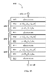
contiguous picocrystalline silaborane p-(Bi2H4)3Si5 regions and
picocrystalline
oxysilaborane p-0312-H4)2Si4022+regions intervened by metallic electrodes;
FIG. 22 is an another illustration of the Carnot cycle;
FIG. 23 is an illustration of a proposed quantum thermodynamic cycle;
FIGS. 24 A-D depict energy diagrams illustrating the proposed occupied
electronic energy levels of the artificial nuclei of the first- and second-
nearest
neighbor picocrystalline artificial borane atoms 101 of a pair of conjoined
picocrystalline silaborane p-(Bi2H4)3Si5 and picocrystalline oxysilaborane p-
(312-114)2Si4022+ regions 401 and 402;
CA 03045318 2019-05-28
WO 2018/164746 PCT/US2017/064020
,
,
18
FIGS. 25 A-D depict a proposed spontaneous mobile charge diffusion;
FIGS. 26 A-D further depict a proposed mobile charge diffusion;
FIGS. 27 A-D still further depict a proposed mobile charge diffusion;
FIGS. 28 A-D depict a proposed spectral induction of valence electrons
from intraicosahedral bonding suborbitals into intraicosahedral antibonding
suborbitals in a picocrystalline silaborane p-(B12H4)3Si5 region;
FIGS. 29 A-D depict a proposed self-thermalization of valence electrons in
a picocrystalline silaborane p-(312H4)3Si5 region due to the nuclear electric
quadrupole moment of the natural boron atoms;
FIG. 30 depict a proposed disproportionation in a picocrystalline silaborane
p-(B12H4)3Si5 region;
FIG. 31 is an illustration of a proposed quantum thermodynamic cycle;
FIG. 32 is an illustration of the Earth's energy budget;
FIG. 33 is an illustration of the spectral radiance of a blackbody;
FIG. 34 is a micrograph obtain by high-resolution transmission microscopy
(HRTEM) of a picocrystalline borane solid deposited on monocrystalline
silicon;
FIG. 35 is an HRTEM fast Fourier transform (FFT) image of the mono-
crystalline silicon substrate;
CA 03045318 2019-05-28
WO 2018/164746 PCT/US2017/064020
19
FIG. 36 is an FFT image of the picocrystalline borane solid;
FIG. 37 is a graph in terms of interplanar lattice d-spacings of the HRTEM
diffraction intensity of the monocrystalline substrate;
FIG. 38 is a graph in terms of interplanar lattice d-spacings of the HRTEM
diffraction intensity of the picocrystalline borane solid;
FIG. 39 is a conventional co-20 x-ray diffraction (XRD) pattern of a self-
assembled picocrystalline borane solid;
FIG. 40 is a grazing incidence x-ray diffraction (GIXRD) scan of the same
self-assembled picocrystalline borane solid in FIG. 39;
FIG. 41 is a second grazing incidence x-ray diffraction (GIXRD) scan of the
same self-assembled picocrystalline borane solid scanned in FIG. 39;
FIG. 42 is an illustration of a silaboride film deposited on a donor-doped
region of a monocrystalline substrate;
FIG. 43 is a graph of a GIXRD scan of the picocrystalline silaboride solid of
Example 1;
FIG. 44 is an illustration of an oxysilaborane film deposited over a donor-
doped silicon region in accordance with Example 2;
CA 03045318 2019-05-28
WO 2018/164746 PCT/US2017/064020
FIG. 45 is a conventional (0-20 x-ray diffraction (XRD) pattern of the thin
oxysilaborane solid of Example 2;
FIG. 46 is a graph of a GIXRD scan of the oxysilaborane solid of Example 2;
FIG. 47 is an illustration of a silaborane film deposited on an n-type silicon
substrate in accordance with Example 3;
FIG. 48 is an x-ray photoelectron spectroscopy (XPS) depth profile of the
silaborane film deposited in Example 3;
FIG. 49 is an Auger electron spectroscopy (AES) depth profile of the
silaborane film deposited in Example 3;
FIG. 50 is an illustration of a silaborane film deposited on a p-type silicon
substrate in accordance with Example 4;
FIG. 51 is an x-ray photoelectron spectroscopy (XPS) depth profile of the
silaborane film deposited in Example 4;
FIG. 52 is a linear graph of the current-voltage characteristics of the
silaborane film deposited in Example 4, as measured by an HP-4145 parameter
analyzer with the sweep signals obtained by a mercury probe;
FIG. 53 is a log-log graph of the current-voltage characteristics of the
silaborane film deposited in Example 4, as measured by an HP-4145 parameter
analyzer with the sweep signals obtained by a mercury probe;
CA 03045318 2019-05-28
WO 2018/164746
PCT/US2017/064020
21
FIG. 54 is an illustration of an oxysilaborane film deposited on a p-type
silicon substrate in accordance with Example 5;
FIG. 55 is an x-ray photoelectron spectroscopy (XPS) depth profile of the
oxysilaborane film deposited in Example 5;
FIG. 56 is a linear graph of the current-voltage characteristics of the
oxysilaborane film deposited in Example 5, as measured by an HP-4145
parameter analyzer with the sweep signals obtained by a mercury probe;
FIG. 57 is a log-log graph of the current-voltage characteristics of the
oxysilaborane film deposited in Example 5, as measured by an HP-4145
parameter analyzer with the sweep signals obtained by a mercury probe;
FIG. 58 is an x-ray photoelectron spectroscopy (XPS) depth profile of
another embodiment of an oxysilaborane film deposited per Example 6;
FIG. 59 is a linear graph of the current-voltage characteristics of the
oxysilaborane film characterized in Example 6, as measured by an HP-4145
parameter analyzer with the sweep signals obtained by a mercury probe;
FIG. 60 is a log-log graph of the current-voltage characteristics of the
oxysilaborane film characterized in Example 6, as measured by an HP-4145
parameter analyzer with the sweep signals obtained by a mercury probe;
CA 03045318 2019-05-28
WO 2018/164746
PCT/1JS2017/064020
22
FIG. 61 is an x-ray photoelectron spectroscopy (XPS) depth profile of
yet another embodiment of an oxysilaborane film deposited per Example 7;
FIG. 62 is a linear graph of the current-voltage characteristics of the
oxysilaborane film characterized in Example 7, as measured by an HP-4145
parameter analyzer with the sweep signals obtained by a mercury probe;
FIG. 63 is a log-log graph of the current-voltage characteristics of the
oxysilaborane film characterized in Example 7, as measured by an HP-4145
parameter analyzer with the sweep signals obtained by a mercury probe;
FIG. 64 is an x-ray photoelectron spectroscopy (XPS) depth profile of
still another embodiment of an oxysilaborane film deposited in Example 8;
FIG. 65 is a linear graph of the current-voltage characteristics of the
oxysilaborane film characterized in Example 8, as measured by an HP-4145
parameter analyzer with the sweep signals obtained by a mercury probe;
FIG. 66 is a log-log graph of the current-voltage characteristics of the
oxysilaborane film characterized in Example 8, as measured by an HP-4145
parameter analyzer with the sweep signals obtained by a mercury probe;
FIG. 67 is an x-ray photoelectron spectroscopy (XPS) depth profile of
yet still another embodiment of an oxysilaborane film deposited in Example 9;
CA 03045318 2019-05-28
WO 2018/164746 PCT/US2017/064020
23
FIG. 68 is a linear graph of the current-voltage characteristics of the
oxysilaborane film characterized in Example 9, as measured by an HP-4145
parameter analyzer with the sweep signals obtained by a mercury probe;
FIG. 69 is a log-log graph of the current-voltage characteristics of the
oxysilaborane film characterized in Example 9, as measured by an HP-4145
parameter analyzer with the sweep signals obtained by a mercury probe;
FIG. 70 is an illustration of a p-isotype electrochemical rectifier comprising
oxysilaborane film produced in accordance with Example 10;
FIG. 71 is a linear graph of the current-voltage characteristics of the p-
isotype electrochemical rectifier in Example 10, as measured by an HP-4145
parameter analyzer with the sweep signals obtained by microprobes;
FIG. 72 is a linear graph of a different current-voltage range of the p-
isotype electrochemical rectifier in Example 10, as measured by an HP-4145
parameter analyzer with the sweep signals obtained by microprobes;
FIG. 73 is a log-log graph of forward-bias current-voltage characteristics of
the p-isotype electrochemical rectifier in Example 10, as measured by an HP-
4145
parameter analyzer with the sweep signals obtained by microprobes;
FIG. 74 is a log-log graph of reverse-bias current-voltage characteristics of
the p-isotype electrochemical rectifier in Example 10, as measured by an HP-
4145
parameter analyzer with the sweep signals obtained by microprobes;
CA 03045318 2019-05-28
WO 2018/164746 PCT/US2017/064020
. .
24
FIG. 75 is a linear graph of the current-voltage characteristics of the p-
isotype electrochemical rectifier in Example 11, as measured by an HP-4145
parameter analyzer with the sweep signals obtained by microprobes;
FIG. 76 is a linear graph of a different current-voltage range of the p-
isotype electrochemical rectifier in Example 11, as measured by an HP-4145
parameter analyzer with the sweep signals obtained by microprobes;
FIG. 77 is a log-log graph of forward-bias current-voltage characteristics of
the p-isotype electrochemical rectifier in Example 11, as measured by an HP-
4145
parameter analyzer with the sweep signals obtained by microprobes;
FIG. 78 is a log-log graph of reverse-bias current-voltage characteristics of
the p-isotype electrochemical rectifier in Example 11, as measured by an HP-
4145
parameter analyzer with the sweep signals obtained by microprobes;
FIG. 79 is a linear graph of a first current-voltage range of the p-isotype
electrochemical rectifier in Example 12, as measured by an HP-4145 parameter
analyzer with the sweep signals obtained by means of microprobes;
FIG. 80 is a linear graph of a second current-voltage range of the p-isotype
electrochemical rectifier in Example 12, as measured by an HP-4145 parameter
analyzer with the sweep signals obtained by means of microprobes;
CA 03045318 2019-05-28
WO 2018/164746 PCT/US2017/064020
FIG. 81 is a linear graph of a third current-voltage range of the p-isotype
electrochemical rectifier in Example 12, as measured by an HP-4145 parameter
analyzer with the sweep signals obtained by means of microprobes;
FIG. 82 is a log-log graph of forward-bias current-voltage characteristics of
the p-isotype electrochemical rectifier in Example 12, as measured by an HP-
4145
parameter analyzer with the sweep signals obtained by microprobes;
FIG. 83 is a log-log graph of reverse-bias current-voltage characteristics of
the p-isotype electrochemical rectifier in Example 12, as measured by an HP-
4145
parameter analyzer with the sweep signals obtained by microprobes;
FIG. 84 is an illustration of an electrochemical device comprising a
silaborane film produced in accordance with Example 13;
FIG. 85 is a linear graph of the current-voltage characteristics of the
electrochemical device in Example 13, as measured by an HP-4145 parameter
analyzer with the sweep signals obtained by microprobes;
FIG. 86 is a linear graph of a second current-voltage characteristics of the
electrochemical device in Example 13, as measured by an HP-4145 parameter
analyzer with the sweep signals obtained by microprobes;
FIG. 87 is a log-log graph of forward-bias current-voltage characteristics of
the electrochemical device in Example 13, as measured by an HP-4145 parameter
analyzer with the sweep signals obtained by microprobes;
CA 03045318 2019-05-28
WO 2018/164746 PCT/US2017/064020
26
FIG. 88 is a log-log graph of reverse-bias current-voltage characteristics of
the electrochemical device in Example 13, as measured by an HP-4145 parameter
analyzer with the sweep signals obtained by microprobes;
FIG. 89 is an illustration of an oxysilaborane film deposited on a p-type
silicon substrate in accordance with Example 14;
FIG. 90 is an x-ray photoelectron spectroscopy (XPS) depth profile of the
oxysilaborane film deposited in Example 14;
FIG. 91 is an illustration of the thermal processing budget of the
oxysilaborane film deposited in Example 14;
FIG. 92 is a geometric representation of an energy equilibration proposed
by Josiah Willard Gibbs;
FIG. 93 is a geometric representation of an entropy equilibration proposed
by Josiah Willard Gibbs;
FIGS. 94 A-B is an illustration comparing a phonovoltaic cell and a
photovoltaic cell in the dark;
FIGS. 95 A-B is an illustration comparing a phonovoltaic cell and a
photovoltaic cell in which mobile electron-hole pairs are radiatively induced;
FIGS. 96 A-B is an illustration comparing a phonovoltaic cell and a
photovoltaic cell in which induced mobile electron-hole pairs are separated;
CA 03045318 2019-05-28
WO 2018/164746 PCT/US2017/064020
27
FIGS. 97 A-B is an illustration comparing a phonovoltaic cell and a
photovoltaic cell in which an electrical load is impressed;
FIGS. 98 A-B is projected manufacturing cost analysis of a phonovoltaic cell;
FIGS. 99 A-B is an illustration comparing a phonovoltaic cell, a
photovoltaic cell, and a thermionic converter;
FIG. 100 is an illustration of a device comprising an oxysilaborane film
and gold produced in accordance with Example 15;
FIG. 101 is an x-ray photoelectron spectroscopy (XPS) depth profile of the
oxysilaborane film deposited in Example 15;
FIG. 102 is secondary ion mass spectroscopy (SIMS) performed to measure
a trace impurity concentration of gold in the oxysilaborane film in Example
15;
FIG. 103 depicts metal electrodes 536 and 537 evaporated over the gold
film containing device of Example 15;
FIG. 104 is a linear graph of the current-voltage characteristics of the
oxysilaborane film in Example 15;
CA 03045318 2019-05-28
WO 2018/164746 PCT/US2017/064020
28
DESCRIPTION OF THE PREFERRED EMBODIMENTS
[0044]
Referring now to the drawings, various forms and embodiments of the
invention will be described. The invention is not to be limited by any
principles or
embodiments described herein, but only by the scope of the appended claims.
[0045] In
order to comprehend the quantum entanglement of the artificial
nuclei of this invention, a regular icosahedron is inscribed in a cube in FIG.
4 such
that the coordinates of the icosahedral vertices are described, subject to Eq.
(21), in
terms of the following position coordinates: ( 0, 1,0), (0, 0, 1), and (
1,0, 0).
¨ 1 = -1 = 2 sin72 0.618
(21)
[0046]
Per the normal crystallographic convention, any orientation along, or
parallel to, any cubic edge is generally represented by (100). Any particular
(100)
orientation, e.g. the [010] orientation along the positive y-axis, will be
specifically
denoted. A cubic face, or a plane parallel to a cubic face, is generally
represented
by {100}. A particular {100} plane, e.g. the xz-plane normal to the [010]
direction,
is represented by (010). A particular (100) orientation, e.g. the [010]
orientation, is
always normal to the corresponding {100} plane, viz. the (010) plane in this
case.
By further convention, any orientation along, or parallel to, a cubic body
diagonal
is represented by (111). There are two classes of icosahedral faces: 8
icosahedral
faces are constituted by {111} planes normal to a (111) cubic body diagonal
and 12
icosahedral faces are constituted by {0 0-10} planes intersecting in pairs
along a
(100) orientation. Three-center bonds exist along edges of the 11111 planes.
CA 03045318 2019-05-28
WO 2018/164746 PCT/US2017/064020
29
[0047]
In connection with the invention described here, a molecular orbital
analysis, which describes the three-center boron bonds by a generalization of
the
methodology of Longuet-Higgins and Roberts performed in [0020110063] of U.S.
Provisional Application No. 62/591,848, is incorporated herein by reference.
That
generalized molecular orbital analysis describes a regular boron icosahedron
104
comprising 12 boron nuclei 102, with a nearly-symmetrical nuclear
configuration,
that is constituted by 24 delocalized atomic orbitals /Pi(Pi
in a nearly-spherical
spheroid wherein displacement is ideally limited to the 8 li(1n) wave vectors.
The
boron icosahedron 104 in FIG. 5 is referred to herein as an artificial nucleus
104.
100481
As used herein, short-range periodic translational order is defined as
a regular repetition of atomic positions over a space substantially confined
to only
first- and second-nearest neighbor atoms. The artificial nucleus 104
represented
in FIG. 5 exhibits a short-range periodic translational order in which the 12
boron
nuclei 102 ideally remain stationary at the 12 icosahedral vertices, such that
all
icosahedral displacement is ideally limited to only periodic vibrations along
the 8
kilo wave vectors. As the result, the artificial nucleus 104 in FIG. 5
constitutes a
quantum Floquet-many-body subsystem that behaves similar to the nucleus of a
natural carbon atom. As used herein, a quantum Floquet-many-body system is a
time-dependent many-body system that is periodic over time by virtue of its
own
dynamics. In order to understand preferred embodiments of this invention, it
is
purposeful to establish the quantum entanglement of the atomic orbitals
zpi(ptia
forming the quantum Floquet-many-body subsystem of the artificial nucleus 104.
CA 03045318 2019-05-28
WO 2018/164746 PCT/US2017/064020
100491 The analysis of the artificial nucleus 104 in FIG. 5 was performed
in
terms of the group analysis of a regular icosahedron. The icosahedral symmetry
group .4 is unique amongst all the other symmetry groups in that it possesses
the
largest number of symmetry operations (120) of any symmetry group in Nature.
The largest number of symmetry operations allowed in any crystallographic
point
group is 48, such that the icosahedral symmetry group /his not a
crystallographic
point group that can support spatial crystals which exhibit a long-range
periodic
translational order. The inability of the icosahedral symmetry group 'h to
support
a long-range periodic translational order allows it to, more generally,
support an
intrinsic spontaneous time-translational symmetry breaking to be described.
100501 It is for this reason that the foregoing symmetry analysis gave
rise to
rectilinear vibrations along the kin) wave vectors of the artificial nucleus
104 in
FIG. 5. The believed energy levels of the 12 boron nuclei 102 forming the
artificial
nucleus 104 are shown in FIG. 6. The energy levels of the 36 valence electrons
of
the artificial nucleus 104 are shown in FIG. 7. The nuclear energy levels in
FIG. 6
and the electronic energy levels in FIG. 7 satisfy the energy eigenvalues of
Dirac's
relativistic wave equation. It is believed that the artificial nucleus 104
shown in
FIG. 5 constitutes a quantum Floquet-many-body system analogous to that of the
natural nucleus of carbon 126C. It is for this reason the 12 boron nuclei 102
of the
artificial nucleus 104 occupy energy levels in FIG. 6 which possess the same
sym-
metry as the energy levels of nucleons in carbonle. The valence electron
energy
levels in FIG. 7 are believed to be similar to the quark energy levels of
carbon 'C.
CA 03045318 2019-05-28
WO 2018/164746 PCT/US2017/064020
31
10051] The artificial nucleus 104 in FIG.5 constitutes a manifestation of
the
quantum Floquet-many-body fermion system with the highest possible degree of
symmetry in Nature. As used herein, a fermion is a subatomic particle, subject
to
the Pauli exclusion principle, which is characterized by Fermi-Dirac
statistics, as
well as, any composite particle comprised of an odd number of said subatomic
par-
ticles. By definition, a quantum Floquet-many-body system comprising fermions
at the vertices of a regular icosahedron will be hereinafter referred to as an
icosa-
hedral Floquet-many-fermion system. In compliance with this definition, the 12
boron nuclei 102 of the artificial nucleus 104 are initially assumed to be
boron m5B
nuclei comprising an odd number of both protons and neutrons. An incorporation
of the other natural boron isotope 1B will be later considered hereinbelow.
100521 The icosahedral Floquet-many-fermion system of the particular arti-
ficial nucleus 104 in FIG. 5 possesses the highest degree of degree of
symmetry in
Nature relative to the icosahedral vertices at which the 12 boron nuclei 102
reside.
This symmetry is exhibited by the 12 nucleons of carbon126C. There exist only
two
types of point displacement, viz, translation along a rectilinear axis and
rotation
about a rectilinear axis. Translation and rotation exhibit contrary
displacements
of points, such as the twelve icosahedral vertices of an icosahedral Floquet-
many-
fermion system. All points along a rectilinear axis of translation, and only
these
points, are displaced under a given translation; conversely, all points not
along a
rectilinear axis of rotation, and only these points, are displaced under any
given
rotation. Rotation complicates the analysis of a quantum many-body system.
CA 03045318 2019-05-28
WO 2018/164746 PCT/US2017/064020
32
100531
As further described in 100201100631 of U. S. Provisional Application
No. 62/591,848 and incorporated herein by reference, the 3 corotating
Cartesian
axes (x,y,z) of an icosahedron are best represented in terms of Miller
indices. Due
to the corotating Cartesian axes (x,y,z), it is not possible to describe the
displace-
ment of the 12 icosahedral vertices in the laboratory frame field. By a
symmetry
analysis, it was established that the icosahedral vertices of the artificial
nucleus
104 in FIG. 5 are motionless and that all icosahedral displacement is confined
to
rectilinear translation along four pairs of inverted k(111) wave vectors.
k[111] < > k111l (22a)
k[111] < > k[iill (22b)
< __ > 11[1111 (22c)
k[1ii] < > ki] (22d)
100541
Said analysis concluded that the 12 boron nuclei 102 are confined to
the motionless icosahedral vertices of the artificial nucleus 104, which,
therefore,
behaves as a nearly-spherical spheroid that is predisposed to be displaced
along
well-defined spherical harmonics. As further described in [0170110207] of U.
S.
Provisional Application No. 62/591,848 and incorporated herein by reference,
any
nearly-spherical spheroid is separated into zones by the spherical harmonics.
The
dipole spherical harmonics associated with the rt.= 1 shells in FIG. 6
separate a
nearly-spherical spheroid into a pair of hemispheres by an equatorial great
circle.
The center-of-mass (or centroid) associated with the dipole spherical
harmonics
is not motionless. The quadrupole spherical harmonics associated with the n =
2
shells in FIG. 6 separate a nearly-spherical spheroid into a pair of great
circles.
CA 03045318 2019-05-28
WO 2018/164746 PCT/US2017/064020
. , .
33
[0055] The great circles associated with the quadrupole spherical
harmonics
contain the lion) wave vectors of the artificial nucleus 104 in FIG. 5. This
is con-
sistent with the displacement of an icosahedral Floquet-many-fermion system in
Eqs. (22 a-d). The symmetry analysis of the artificial nucleus 104 in FIG. 5
is of a
general nature, without any commitment as to the physical size of the
icosahedral
Floquet-many-fermion system. The distance between opposite icosahedral faces
of the artificial nucleus 104 is ideally 269 pm, such that it is specifically
referred
to as an icosahedral Floquet-many-fermion picocrystal. The distance between
the
opposite icosahedral faces of the natural nucleus of carbon 1C can be measured
in
terms of femtometers, such that the natural nucleus of carbon 126C constitutes
an
icosahedral Floquet-many-fermion femtocrystal. It is believed that the
artificial
nucleus 104 exhibits the same symmetry as the natural nucleus of carbon 'C.
[0056] An icosahedral Floquet-thany-fermion picocrystal (femtocrystal)
lifts
the intraicosahedral electronic (quark) orbital degeneracies by way of a spin-
orbit
coupling, so as to escape Jahn-Teller distortion. In the landmark paper
"Stability
of Polyatomic Molecules in Degenerate Electronic States. I. Orbital
Degeneracy,"
Proceedings of the Royal Society A, 161, 1937, pp. 220-235, H. A. Jahn and E.
Teller
developed by means of group theory that: All nonlinear nuclear configurations
are
unsuitable for an orbitally-degenerate electronic state. The Jahn-Teller
effect re-
sults in a symmetry-breaking that lifts electronic orbital degeneracies by
normal
displacements of the 12 boron nuclei 102, known as Jahn-Teller-active modes,
that
distort polyatomic ions and molecules in the absence of spin-orbit coupling.
CA 03045318 2019-05-28
WO 2018/164746 PCTPUS2017/064020
34
100571 In their analysis, Jahn and Teller intentionally ignored spin
effects.
Spin-orbit coupling is essential to preserving the intraicosahedral bonding of
the
icosahedral Floquet-many-fermion picocrystal of the artificial nucleus 104,
sub-
ject to the intraicosahedral bonding and antibonding orbitals portrayed in
FIG. 7.
Said another way, the quantum entanglement of the electronic eigenstates shown
in FIG. 7 cannot exist in the presence of any Jahn-Teller distortion. By
lifting the
electronic orbital degeneracies by means of spin-orbit coupling - instead of
Jahn-
Teller distortion - quantum entanglement causes the icosahedral Floquet-many-
fermion picocrystal comprising the artificial nucleus 104 to physically behave
as
a Planckian resonator that can be chemically modified in novel and useful ways
by controlled variations in the quantum entanglement of the energy levels.
100581 In order to practice preferred embodiments of the present
invention,
it is purposeful to cogently consider certain elements of the icosahedral
Floquet-
many-fermion picocrystal comprising the artificial nucleus 104 shown in FIG.
5.
Preferred embodiments of the invention constitute novel and useful embodiments
of a quantum thermodynamics capable of supporting a quantum thermodynamic
cycle that self-thermalizes, so as to eliminate the dependence of a heat
engine on
fuels. The novel and useful embodiments of this invention cannot be described
by
means of classical thermodynamics due to the role of quantum entanglement. In
order to describe preferred embodiments of this invention, it is necessary to
draw
on predictions of Dirac's wave equation. The first-principles are disclosed in
U. S.
Provisional Application No. 62/591,848 and are incorporated herein by
reference.
CA 03045318 2019-05-28
WO 2018/164746 PCT/US2017/064020
[0059]
Considerable effort has been devoted, by reference, to the symmetry
operations of the icosahedral Floquet-many-fermion picocrystal of the
artificial
nucleus 104. This is due to the belief that the symmetry of the artificial
nucleus
104 endows it novel and useful properties that are unique to this specific
type of
quantum many-body system. The derivation of Einstein's E= mc2, by the special
theory of relativity, governs the loss of inertia of a uniformly-translating
body. By
virtue of this derivation, Einstein established that energy E and mass m are,
in
actuality, two "phases" of the same quantity. Einstein formed this conclusion
by a
consideration of the relativistic translational Doppler shift of a radiative
body. In
extending his special theory of relativity to include rotation in his general
theory
of relativity, Einstein was unable to derive a relativistic rotational Doppler
shift.
[0060]
Since a rotating fermion necessarily emits radiation, then a rotating
fermion can only stabilize as a member of a quantum many-body system in which
pairs of complementary rotational Doppler shifts stabilize said quantum many-
body system. The icosahedral Floquet-many-fermion picocrystal of the
artificial
nucleus 104 constitutes a stabilized quantum many-body system of fermions that
can be described by Dirac's relativistic wave equation. Dirac's energy
eigenvalues
for a Dirac many-body system of fermions obtained within 10086140167] of U. S.
Provisional Application No. 62/591,848 are incorporated herein by reference.
a2mc2 a4mc2 n +1, +2, +3, ...
¨ < mc2
(23 a)
2n2 27cri3
E=
_mc2 a2mc2+ a4mc2 > -mc2 {- = 1, 2, , +n
(23b)
2n2 2Kn3 It = ¨1, ¨2, ¨3, ...
CA 03045318 2019-05-28
WO 2018/164746 PCT/US2017/064020
36
[0061] The positive-energy eigenstates of the antibonding suborbitals in
Eq.
(23a) and the negative-energy eigenstates of the bonding suborbitals in Eq.
(23b)
of the artificial nucleus 104 shown in FIG. 5 are tabulated below.
Table 1: Antibonding suborbitals of the artificial nucleus 104
orbital spin-orbital radial harmonics hcoK vK
n n
n cr=L N multipole eV
GHz
+1 0 +ls ,e+1/2 1/2 +181,2 -(t+1) -1 +isi/2 dipole 0 0
+1/2 3/2 +2p312 -(t+1) -2 +2p312 quadrupole 45.3 10.9
+2 1 +2p
-1/2 1/2 +2P1n t +1
+2spin inner lobes 0 0
+2 0 +2s f+1/2 1/2 +2s112 ¨(t+1) ¨1
t+1/2 5/2 +3d512 +1) -3 +3d5,2 octupole
17.9 4.31
+3 2+3d
t-V2 3/2 +3d312 t +2
+3pd3/2 inner lobes 13.4 3.22
,e+1/2 3/2 +3p312 -(t+1) -2
+3 1 +3p
t-1/2 1/2 d-3P1/2 t +1
+3 sp 1/2 inner lobes 0 0
+3 0 3s e+% 1/2 +3s112 -(t+1) -1
Table 2: Bonding suborbitals of the artificial nucleus 104
orbital spin-orbital radial harmonics
hcoK vK
n n
n cr=L j1K1 K multipole eV
GHz
¨1 0 ¨1s i--1/2 1/2 -1s112 t +1 -1s1/2 dipole 0
0
t-1/2 3/2 -2p312 t +2 , -2p3/2 quadrupole
45.3 10.9
-2 1 -2p
t+1/2 1/2 -2p112 - +1) -1
-2sp1/2 inner lobes 0 0
-2 0 -2s i-1/2 1/2 -2s1/2 t +1
t-% 5/2 -3d512 +3 -3d512 octupole
17.9 4.31
-3 2 -3d
t+1/2 3/2 -3d3,2 -(t+1) -2
-3pd3/2 inner lobes 13.4 3.22
i-1/2 3/2 -3p312 t +2
-3 1 -3p
+1/2 1/2 -3/3112 -U-F1) ¨1
-3sP1/2 inner lobes 0 0
-3 0 -3s t-1/2 1/2 -3s112 t +1
CA 03045318 2019-05-28
WO 2018/164746 PCT/1JS2017/064020
37
[00621
Spin-orbit coupling lifts the orbitally-degenerate energy orbitals into
the half-integer-quantized antibonding suborbitals with a positive-definite
energy
per Table 1. Spin-orbit coupling lifts orbitally-degenerate energy orbitals
into half-
integer-quantized bonding suborbitals of a negative-definite energy per Table
2.
The antibonding and bonding suborbitals for both the n = 2 and n = 3 shells
of
the artificial nucleus 104, subject to Eqs. (23 a-b), are shown in FIG. 7. The
n = 1
shells are not shown since they contain inner electrons not involved in the
fusion
of the artificial nucleus 104. There are several significant aspects of the
bonding
and the antibonding suborbitals of the artificial nucleus 104 in FIG. 7. Spin-
orbit
coupling lifts orbital degeneracies, as exemplified below for the n = +2
shell.
rft
+2p (.e =1)ed shi> +2p3/2(i = + <=> K = (t + 1) = ¨2
(24a)
blue shift
+2p(t =1) > +21)1120 = t--1/2)
.4=> = + = +1 (24b)
red shift
+2SQ=0) ¨) +2 sin(j = +1/2)
<=>ic = ¨(+ 1) = ¨1 (24c)
[00631
The +2p orbital is subjected to both a Doppler red-shift = ¨2) into a
+2p3/2 suborbital and Doppler blue-shift (K= +i) into a +2p112 suborbital. The
+2s
orbital is subjected to a Doppler red-shift (K = ¨1) into a +2 s1,2
suborbital, which, in
turn, is entangled with the +2p112 suborbital, so as to thereby result in the
+2sp112
suborbital (x = 1). These are rotational Doppler shifts that are
incomprehensible
by E =mc2. Einstein derived his E = mc2 in a follow-up paper to his seminal
paper
that initially introduced the special theory of relativity: "On the
Electrodynamics
of Moving Bodies," 1905, in The Principle of Relativity, Dover, 1952, pp. 37-
65.
CA 03045318 2019-05-28
WO 2018/164746 PCT/US2017/064020
38
[00641
Fusion is generally taken herein to be any process in which fermions
are bonded together by the transformation of a quantity of matter m into
energy.
Einstein's E = mc2 is widely assumed to govern a nuclear fusion in which
nucleons
are bonded together by the transformation of a small quantity of matter m into
an
energy E manifested in the form of photons. By generalizing Einstein's E = mc2
in
a rotating frame field, a heretofore-unknown chemical fusion can be
established
by atoms chemically bonded together by the transformation of a small quantity
of
matter m into some energy E of a Dirac quasiparticle. For the purposes at
hand, a
Dirac quasiparticle is a quantum Floquet-many-fermion system due to a dynamic
interaction between fermions that entangles the individual energy levels.
100651
The quantum entanglement of the artificial nucleus 104 in FIG. 5 is
associated with the entangled eigenfunctions /PO (
due to chemical fusion. No
attempt is made to directly claim a generalization of Einstein's E = mc2 to
support
chemical fusion. Present focus is on the real-world application of chemical
fusion.
Pursuant to this objective, the relations in Eqs. (23 a-b) are rearranged as
follows
in order to frame the generalization of Einstein's E = mc2. These relations
specify
the energy eigenvalues of a Dirac quasiparticle in Dirac's forbidden energy
region
mc2 > E> ¨mc2, with entangled positive-energy (E> 0) and negative-energy (E <
0)
eigenstates that comprise the antibonding and bonding suborbitals.
mc2 ¨E ¨ +a2mc2 ct4mc2
>0 E >0
(25a)
2n2 27cn3
ct2mc2 a4mc2
¨Mc2 ¨E = ____________________________ <0 E < 0
(25b)
2n2 2wn3
CA 03045318 2019-05-28
WO 2018/164746 PCT/US2017/064020
39
[0066]
Were Einstein's E = mc2 to be satisfied in a rotating frame field, then
the bound-energy terms on the right side of Eqs. (25 a-b) would vanish - since
the
energy eigenstates in Eq. (25b) are negative-definite (E < 0). The first term
on the
right side of Eq. (25a) comprises energy eigenvalues obeying Schrodinger's
wave
equation. For the present purposes, it is sufficient that the highest bound-
energy
eigenstates satisfying Schrodinger's wave equation exist in the n = +1 shell.
The
successive higher-order shells thus comprise lower bound-energy eigenstates.
The
orbital angular momentum remains degenerate in the bound-energy eigenstates
obeying Schrodinger's equation. This degeneracy is lifted by Dirac's equation.
[0067]
The second bound-energy term on the right side of Eq. (25a) is due to
the fine structure of a spinning fermion. The salient properties of a fermion
fine
structure are cogently described in order to better understand real-world
devices
comprising preferred embodiments of this invention. Pursuant to this
particular
objective, the energy eigenvalues of a Dirac quasiparticle, per Eqs. (25a-b),
are re-
arranged below for the n = 2 and n = 3 shells of a quantum many-body system.
2 4 n = +1, +2, +3
mc2 -E = mc2 [a + 1> 0
(26 a)
2n2 2Kn3 K = T1, ;2, ,-n
4 = 1, 2, , +n
+E = rno[ a2 a 1>0 (26b)
2n2 21cn3 n = -1, -2, -3
[0068]
Whereas the quantity of matter of the reactants and products is in-
variant in classical chemistry, quantum chemistry involves a finite variation
in
the quantity of matter of the chemical reactants and products due to fusion.
The
role of quantum chemistry in this invention will be further discussed below.
CA 03045318 2019-05-28
WO 2018/164746 PCT/US2017/064020
=
[0069]
Since neither energy E nor mass m is actually conserved, then there
must exist another conserved physical entity that wholly contains energy E and
mass m. Electric charge e is rigorously conserved in Nature. Although not
known
in the prior art, the strict conservation of electric charge e results in a
heretofore-
unknown physical entity E = ec2 that wholly contains Einstein's E = mc2.
'= ec2 E = mc2
(27)
[0070]
The new entity E = ec2 is named apeiron, which is a transliteration of
the Greek word duceipm meaning "boundless." The concept of apeiron was
initially
conceived by Anaximander of Miletus circa 585 BC. The ability to exploit
electric
charge e in a quantum thermodynamic cycle, capable of replacing a Carnot
cycle,
can only be achieved when electric charge e is provided a mechanical basis.
The
mechanical basis of electric charge e is fundamentally derived in [07941-
10846] of
U. S. Provisional Application No. 62/591,848 and incorporated herein by
reference.
e = = 1.7588363 x 10-43 kg.m
(28)
2c
100711 The MKS equivalent of a coulomb C follows from the above relation.
1C = 1.09778 x 10⁻²⁴ kg.m (29)
100721
The following relationship is believed to govern the resonator of the
icosahedral Floquet-many-fermion picocrystal of the artificial nucleus 104 as
well
as the icosahedral Floquet-many-fermion femtocrystal of the carbon 1C nucleus.
Apeiron E = ec2 and Kirchhoff's universal function K(v,T) can be related.
hc
= ec2 = mc2-2 = hcol =
(30)
2 2
CA 03045318 2019-05-28
WO 2018/164746 PCT/US2017/064020
41
100731
Wilhelm Wien actually derived his blackbody radiation law from the
perspective of the resonator by way of two very important papers. In 1893,
Wien
derived his namesake spectral displacement law, which bears directly on
certain
preferred embodiments of this present invention. A derivation of Wien's
spectral
displacement law is carried out in a modern formulation in [0931]-[09961 of
U.S.
Provisional Application No. 62/591,848 and is incorporated herein by
reference.
Wien derived his spectral displacement law by considering the mechanical work
done on electromagnetic radiation, which is manifested in two ways: (1)
radiative
energy is spectrally displaced from the lower-frequency interval (v,v+dv) into
the
higher-frequency interval (vi,vid- dv') and (2) work further introduces energy
in the
higher-frequency interval (V,V+dv'). The total energy lExH lin dA dt entering
into
the higher-frequency interval is expressed by the following relation:
27r
I E xH lin dA dt = 0K(v,T) dv cose dO dA dt + dF dt
2,7r
= dv + 2 icoselcosoc152 dA dt
0
2 7r
= I K(v, T) dv' cos dA dt
(31)
Jo
100741 As
actually derived in [0931110996] of U.S. Provisional Application
No. 62/591,848 and incorporated herein by reference, Wien's spectral
displacement
law supports the following spectral displacement (i.e., a shift in frequency)
at the
constant irradiance ExHI that is characteristic of blackbody radiation.
Spectral
displacement is capable of quantum mechanically supporting a heat engine.
hv' = hv[1+ 24 cos0] = lExHiv
(32)
CA 03045318 2019-05-28
WO 2018/164746 PCT/US2017/064020
42
[0075] In
Eq. (32), A is the phase velocity of electromagnetic radiation. For a
positive phase velocity A > 0, work is done upon electromagnetic radiation in
order
to cause it to undergo a spectral displacement from some lower frequency
interval
(v,v+dv) into a higher frequency interval (V,V+ dv'). Such a spectral
displacement
results in the increase in radiative energy at a constant irradiance IE xH I,
which
is significant in that the irradiance of blackbody radiation uniquely
corresponds
to the radiator temperature in thermal equilibrium. Such a capability is built
into
Wien's blackbody radiation law, albeit in a way that is not known in the prior
art.
A form of Wien's blackbody radiation law was given hereinabove in Eq. (18).
-8--7rv2 hv e-hvAT dv
u(v,T)dv = hv kT
(18)
c3
100761 Wien's blackbody radiation law supports the following relation.
X hc X _ X
hv¨ = hv'¨ = ¨ = hu)'¨X = h ¨ w¨ hco4n
(33)
2 2 2 2 2
[0077] Over an entire solid angle, Kirchhoff's universal function K(v,T)
is:
v2 K(v,T) = u(v,T) ¨ 2 hv
(34)
47r c2 ehvileT _1
[0078]
Near the ultraviolet blackbody radiation extreme hv kT, Kirchhoff's
universal function K(v,T) is dependent upon electric charge e so as to thus
exhibit
a dependency upon apeiron = ec2 in accordance with the following relation that
can be applied to the artificial nucleus 104. The boron nuclei 102 of the
artificial
nucleus 104 are packed sufficiently close together that the boron nuclei 102
are
radiatively coupled to form a self-assembled picocrystalline radiation cavity.
3
K(v,T) = 8yrec211-- e¨hvIkT 2-12. hv e¨hvikT hv kT
(35)
c3 c2
CA 03045318 2019-05-28
WO 2018/164746 PCT/US2017/064020
43
[0079]
Kirchhoff's universal function K(v,T) at the infrared spectral extreme
hv<<kTis dominated by the continuous thermal resonator energy kT while, very
differently, Kirchhoff's universal function K(v,T) near the ultraviolet
spectral ex-
treme hv>> kT is dominated by the discrete vibrational energy hv.
K(v, T) = 2 -V-2 kT hv kT
(36a)
c2
2
MVA, = 2[] hv g exp ¨hvg hvK kT
(36b)
kT
[0080] It
is purposeful to express Planck's resonator entropy S in Eq. (12) in
terms of discrete energy elements hv g obeying Dirac's relativistic wave
equation.
S= k ln Ul ¨ U ln U
(37)
hvg hvg, hvg hvg
[0081] It
is purposeful to define the quantum temperature eT in accordance
with Planck's relation in Eq. (13), subject to the quantization in Eq. (36b).
(38)
OT au F
hvg U
[0082]
Einstein's molar heat capacity in Eq. (20) can be simplified as follows
for a low-frequency Planckian resonator frequency, such that hv kT.
Cmoiar = 3R[1+ hv kT (39)
kT
[0083]
The heat capacity associated with a microwave Planckian resonator
of an individual atom in a solid governed by Dirac's relativistic wave
equation is
described by the following relation derived from Einstein's molar heat
capacity.
= 3 k[i+ hvg]
hvg kT
(40)
kT
CA 03045318 2019-05-28
WO 2018/164746 PCT/US2017/064020
,
44
[0084] As shown in FIG. 8, a picocrystalline artificial borane atom 101
con-
stitutes: (1) an artificial nucleus 104 formed by a boron icosahedron
comprising
12 natural boron nuclei 102 with a nearly-symmetrical nuclear configuration
and
(2) 4 artificial valence electrons constituted by 4 natural hydrogen atoms
with the
hydrogen nuclei 103 bonded to a boron icosahedron such that the 4 hydrogen val-
ence electrons are aligned along a li(111) wave vector. The picocrystalline
artificial
borane atom 101 comprises a boron icosahedron with 36 boron valence electrons
occupying intraicosahedral molecular orbitals, such that intericosahedral
chemi-
cal bonds are by the hydrogen valence electrons. An electric quadrupole moment
along the k(111) vectors causes an electric dipole moment in hydrogen atoms,
such
that the hydrogen nuclei 103 bond by a Debye force to the artificial nucleus
104.
[0085] A chemical bonding of the picocrystalline artificial borane atoms
101
is explained by a self-selective atomic replacement in the monocrystalline
silicon
unit cell 200 in FIG. 9, which is comprised of 8 silicon vertex atoms 201, 6
silicon
face-center atoms 202, as well as, 4 silicon basis atoms 203. The 4 basis
atoms 203
reside along a (11.1) cubic body diagonal in a tetrahedral arrangement. The
mono-
crystalline silicon unit cell 200 is periodically translated over space so as
to form a
monocrystalline silicon lattice wherein the silicon vertex atoms 201 and the
silicon
face-center atoms 202 are covalently bonded to, and only to, the four silicon
basis
atoms 203 along a (111) crystal orientation. The resultant monocrystalline
silicon
lattice has a long-range periodic translational order in terms of cubic unit
cells of
¨0.5431 nm along each edge, without any (100) chemical bonds.
CA 03045318 2019-05-28
WO 2018/164746 PCT/US2017/064020
10086] A diamond-like picocrystalline silaborane unit cell 300 is
constructed
by replacing each silicon vertex atom 201 within the monocrystalline silicon
unit
cell 200 with a borane molecule 101, as shown in FIG. 10. The 8 borane
molecules
101 at the vertices of the silaborane unit cell 300 in FIG. 10 are shared
amongst 8
picocrystalline silaborane unit cells 300 in an extended solid lattice (not
shown).
The periodic translation of the picocrystalline silaborane unit cell 300 over
space
would, thereby, result in a picocrystalline silaborane (B12H4)Si7 solid
lattice that
effectively acts as a self-assembled diamond-like picocrystalline lattice
structur-
ally similar to monocrystalline silicon. Picocrystalline artificial borane
atoms 101
in FIG. 8, with a nearly-symmetrical nuclear configuration, replace the 8
silicon
vertex atoms 201 in FIG. 10 in the picocrystalline silaborane (B12H4)Si7
lattice.
100871 The picocrystalline oxysilaboranes of this invention constitute
nearly
transparent solids that are believed to be formed by a continuous random
network
of polyatomic unit cells obeying a modification of rules developed by
Zachariasen
in a paper "The Atomic Arrangement in Glass," Journal of the American Chemical
Society, Vol. 54, 1932, pp. 3841-3851. All references hereinafter to
Zachariasen are
understood as referring to this paper. Zachariasen focused on oxide glasses
and,
more particularly, on amorphous SiO2 and amorphous B203. Zachariasen proved
that amorphous SiO2 is constituted by a continuous random network of SiO4
tetra-
hedra. Similarly, the picocrystalline oxysilaboranes are believed to be
constituted
by the continuous random network of polyhedra with a nearly-symmetrical boron
icosahedron at each of the eight polyhedra corners.
CA 03045318 2019-05-28
WO 2018/164746 PCT/US2017/064020
46
[0088] Whereas usual oxide glasses are constituted by a continuous random
network of oxygen tetrahedra or oxygen triangles, picocrystalline
oxysilaboranes
constitute solids formed by the continuous random network of borane hexahedra
which, by definition, are constituted by hexahedra with picocrystalline
artificial
borane atoms 101 at the hexahedral corners. Whereas the monocrystalline
silicon
unit cell 200 portrayed in FIG. 9 is a regular hexahedron (cube), the diamond-
like
picocrystalline silaborane unit cell 300 in FIG. 10, while portrayed for
description
purposes as a cube, is in actuality an irregular hexahedron. Whereas
Zachariasen
represented the atomic arrangement of an oxide glass by the continuous random
network of polymorphic oxygen tetrahedra or triangles, the atomic arrangement
in a borane solid is described by a random network of irregular hexahedra.
100891 The eight corners of the borane hexahedron 300 in FIG. 10 are com-
prised of picocrystalline artificial borane atoms 101. Each corner
picocrystalline
artificial borane atom 101 is, ideally, bonded to four tetravalent natural
atoms 303
which are surrounded by eight corner picocrystalline artificial borane atoms
101.
The preferred tetravalent natural atoms 303 are natural silicon atoms. Each of
the tetravalent natural atoms 303 bonds to one or more face-center atom 302 in
the borane hexahedron 300 shown in FIG. 10. Each face-center atom 302 can be
any of, but not limited to: a tetravalent natural atom such as silicon; a
hexavalent
natural atom such as oxygen; or, possibly, a tetravalent picocrystalline
artificial
borane atom 101. With the help of the irregular borane hexahedron 300 shown in
FIG. 10, the atomic arrangement of a borane solid can be understood.
CA 03045318 2019-05-28
WO 2018/164746 PCT/US2017/064020
47
[0090] First, four tetravalent natural atoms 303 are surrounded by 8
corner
picocrystalline artificial borane atoms 101 in a solid borane lattice.
Secondly, the
conjoined irregular borane hexahedra 300 share common corner picocrystalline
artificial borane atoms 101 within the continuous random network. The centroid
of
the corner picocrystalline artificial borane atoms 101 is, ideally, motion-
invariant.
Thirdly, each corner picocrystalline artificial borane atom 101 covalently
bonds to
four tetravalent natural atoms 303 along a (111) crystalline orientation. It
is note-
worthy to recognize that the tetravalent natural atoms 303 are in the
positions of
the silicon basis atoms 203 (as shown in FIG. 9 in the unit cell of
monocrystalline
silicon) that undergo a spatial displacement to preserve the unit cell
dimension.
10091] The above-described structure can be understood by considering the
believed structure of an extreme, (B12H4)4Si4, of a new genus of the to-be-
defined
picocrystalline oxysilaboranes. In (B12H4)4Si4, each irregular borane
hexahedron
300 forming a solid lattice is ideally constituted by 8 corner picocrystalline
arti-
ficial borane atoms 101, 6 face-center picocrystalline artificial borane atoms
101,
and 4 natural silicon atoms 303. Due to the sharing of 8 hexahedral corners
and
the sharing of 2 hexahedral faces, the translation of irregular borane
hexahedra
300 over space ideally gives rise to picocrystalline silaborane (312H4)4Si4.
In this
manner, picocrystalline silaborane (B12H4)4Si4 forms a picocrystalline
polymorph,
similar to monocrystalline silicon, comprised of tetravalent natural silicon
atoms
303 and tetravalent picocrystalline artificial borane atoms 101. It is by
means of
this type of structure that spin-orbit coupling becomes physically important.
CA 03045318 2019-05-28
WO 2018/164746 PCT/US2017/064020
,
,
48
[0092] Preferred embodiments of this invention involve a type of order not
known in the prior art. Long-range periodic translational order is defined
herein
as the regular repetition of a certain invariant arrangement of atoms, known
as a
unit cell, through space so as to thereby form a translationally-invariant
tiling in
a regular array of natural atoms well beyond first- and second-nearest
neighbor
natural atoms. Monocrystalline and polycrystalline materials exhibit a long-
range
periodic translational order throughout space. The periodic repetition of
atomic
positions is preserved throughout the entire space of a monocrystalline
material.
In a polycrystalline material, the periodic repetition of atomic positions is
main-
tained over the limited finite space in grains, which can be themselves
arbitrarily
oriented over space. As used herein, a nanocrystalline material is any
polycrystal-
line material in which the grain sizes range between 300 pm and 300 nm.
[0093] Short-range periodic translational order is defined hereinafter as
the
repetition of natural atomic positions over a space substantially confined to
only
the first- and second-nearest neighbor natural atoms. The radii of isolated
neutral
atoms range between 30 and 300 pm. As the result, and as used herein, any pico-
crystalline material is a material exhibiting a short-range periodic
translational
order confined to repeating atomic positions in finite groups of first- and
second-
nearest neighbor natural atoms. An amorphous material, as used hereinafter, is
a material void of regularly repeating arrangements of atoms, so as to thus be
in-
capable of supporting a constructive interference of x-rays. Short-range
periodic
translational order is dominant in picocrystalline silaborane (B12114)4Si4.
CA 03045318 2019-05-28
WO 2018/164746 PCT/US2017/064020
49
[0094] It might appear that these definitions of various types of
crystalline
materials completely describe the allowable order of repeating atomic
positions in
space. But, these definitions remain yet limited in the sense that they are
based
strictly upon repeating positions of individual atoms over space. They cannot
be
applied to materials which include tightly packed clusters of atoms arranged
in
space, such that the clusters may themselves be bonded to single natural atoms
which are not so clustered. These definitions must be extended to comprehend a
quantum dot, which is defined, for purposes herein, as a cluster of natural
atoms
in which a discrete quantization of energy levels exists. The size of a
quantum dot
in the prior art is typically on the order of 10 nm. The above noted
definitions of
various types of crystalline solids are also dependent on an energy
quantization.
[00951 This leads to the requirement for a new definition that
comprehends
both the spatial arrangement of atoms and the presence of a discrete
quantization
of energy levels. Therefore, as used herein, a "picocrystalline artificial
atom" is a
cluster, of a size less than 300 pm, of natural atoms that are mutually bonded
to-
gether so as to support a short-range periodic translational order and an
internal
discrete quantization of energy levels. As further described below, special
types of
picocrystalline artificial atoms can be bonded to other natural atoms in order
to
form an extended lattice of natural atoms and picocrystalline artificial
atoms. As
used herein, a natural atom is any isotope of a stable chemical element
contained
in the periodic chart. A special type of picocrystalline artificial atom
comprises a
boron icosahedron with a nearly-symmetrical nuclear configuration.
CA 03045318 2019-05-28
WO 2018/164746 PCT/US2017/064020
[0096] The singular material most responsible for the solid-state
electronic
revolution over the past six decades is monocrystalline silicon. As the
scaling of
feature sizes of monolithic integrated circuits approaches molecular
dimensions,
the displacement of electric charge in extended energy bands over space
increas-
ingly breaks down due to fundamental quantum conditions. In a related manner,
electric charge conduction in extended energy bands in low-dimensional
metallic
interconnects further degrades the performance of monolithic integrated
circuits.
In recent years, there has been extensive research into the incorporation of
mono-
layer graphene in monolithic integrated circuits in a determined effort to
remedy
fundamental scaling limitations. Monolayer graphene presents a challenge to an
incorporation into monolithic integrated circuits due to the absence of a
bandgap
energy and an incompatible deposition process with integrated circuits.
100971 Preferred embodiments of this invention remedy scaling limitations
of monolithic integrated circuits by a material amalgamation of
monocrystalline
silicon and graphene that supports a displacement of electrical action over
space.
Referring, now, to FIG. 10, it can be observed that picocrystalline artificial
borane
atoms 101 replace the silicon vertex atoms 201 in FIG. 10. In the specific
case of
picocrystalline silaborane (B12H4)4Si4, the six face-center atoms 302 are
(although
not shown in FIG. 10) picocrystalline artificial borane atoms 101. Due to the
pre-
servation of a short-range icosahedral symmetry in each picocrystalline
artificial
borane atom 101, picocrystalline silaborane (1312H4)4Si4 does not possess any
long-
range periodic translational order in the manner of monocrystalline silicon.
CA 03045318 2019-05-28
WO 2018/164746 PCT/US2017/064020
51
[00981
Due to the absence of a long-range periodic translational order, pico-
crystalline silaborane (1312H4)4Si4 cannot physically support extended
conduction
and valence energy bands over space. The existence of van der Waals forces
(and
more particularly, Debye forces) between picocrystalline artificial borane
atoms
101 further eliminates extended conduction and valence energy bands over space
in picocrystalline silaborane (B12H4)4Si4. However, the icosahedral symmetry
of
the picocrystalline artificial borane atoms 101 gives rise to a highly novel
type of
displacement of electrical action which is not known in the prior art. In
order to
more fully understand the profound novelty and utility of preferred
embodiments
of this invention, consider the low-frequency extremes of Eqs. (36 a-b).
K(v, T) = 2 --V2 kT hv kT
(41a)
c2
2
K(VA, T) = 2[] 1 hvg c hvg kT
(41b)
[00991 A
Planckian resonator constitutes a hybridization of two resonators:
(1) the thermal resonator with the vibrational energy U= kT and (2) the
quantum
resonator with the vibrational energy U= hvg. The quantum temperature OT of a
discrete quantum resonator with U= hvg is specifically given by Eq. (38) as:
hvg
eT = ----kln 2
(42)
[0100] At
the microwave frequency vg =10.9 GHz in Tables 1-2, the quantum
temperature OT = 0.77 K of the artificial nucleus 104 is well below the
absolute
temperature 2.72 K associated with the cosmic microwave background radiation.
hvg
07(10.9 GHz) = T----ln 2 = 0.77 K
(43)
CA 03045318 2019-05-28
WO 2018/164746 PCT/US2017/064020
,
52
[01011 By contrast, the quantum temperature OT of the continuous thermal
resonator, with U¨ k[ is much greater than the ambient temperature T Since
the artificial nuclei 104 forming picocrystalline silaborane (B12H4)4Si4
constitute
open icosahedral Floquet-many-fermion picocrystals, then the quantum tempera-
ture OT of any artificial nucleus 104 is clamped at the ambient temperature T
In
order to better understand the thermal equilibration of picocrystalline
silaborane
(312114)4Si4, it is purposeful to consider the ordered filling of the
intraicosahedral
antibonding and bonding eigenstates by electrons in accordance with Eqs. (23 a-
b)
and Tables 1-2. The antibonding and bonding energy levels within the n = 2
and
n = 3 shells are greatly exaggerated relative to the forbidden energy region.
[0102] Per FIG.11 four electrons initially occupy the +242 antibonding
sub-
orbital and four electrons initially occupy the ¨242 bonding suborbital of a
Dirac
quasiparticle. Two consequences of FIG. 11 distinguish Dirac quasiparticles
from
fermions obeying Schrodinger's nonrelativistic wave equation. First of all,
there
is a charge-conjugation symmetry between positive-energy electrons in the anti-
bonding suborbitals and negative-energy electrons in the bonding suborbitals
of a
Dirac quasiparticle. No charge-conjugation symmetry exists in a fermion
governed
by Schrodinger's nonrelativistic equation, which assumes all the energy levels
to
be positive-definite. Per Schrodinger's equation, charge conduction in the
valence
energy band formed by bonding orbitals is taken to be due to mobile holes
arising
from electron vacancies. The physical relation between a negative-energy
electron
and a positive-energy hole (electron vacancy) will be later developed.
CA 03045318 2019-05-28
WO 2018/164746 PCT/US2017/064020
53
[0103] Secondly, the higher-angular-momentum suborbitals 2p1/2 are
filled
by electrons while, curiously, the lower-angular-momentum suborbitals 2 sp 12
are
void of electrons per FIG. 11. Spin-orbit coupling creates a doublet of half-
integer-
quantized suborbitals from a whole-integer-quantized orbital, as represented
per
Eqs. (24 a-b). By a yet-unknown natural phenomenon (referred to hereinafter as
spectral induction), it will be shown that the higher-angular-momentum Q =
suborbital of any doublet due to spin-orbit coupling is initially occupied
before the
lower-angular-momentum (j = ,e-1A) suborbital in a Dirac quasiparticle.
Although
spectral induction is not known in the prior art, it is used in the successful
opera-
tion of preferred embodiments of the present invention.
[0104] The bound-energy eigenstates of a Dirac quasip article are
involved in
the chemical fusion of boron icosahedra comprising preferred embodiments of
this
invention. The inner electrons occupying the n = 1 shells are not involved in
the
chemical bonding of the boron icosahedra. As will be established hereinbelow,
the
spectral quantum number w of the electron fine structure is polarized - except
for
the highest bound-energy eigenstate in a shell. It is noteworthy that the
spectral
quantum number K is negative-definite in, and only in, the highest bound-
energy
eigenstate in the n = +2 and n = +3 shells of the positive-energy antibonding
sub-
orbitals of a Dirac quasip article per Eq. (23 a). It is further noteworthy
that the
spectral quantum number x is positive-definite in, and only in, the highest
bound-
energy eigenstate in the n = -2 and n = -3 shells of the negative-energy
bonding
suborbitals of a Dirac quasip article in accordance with Eq. (23b).
CA 03045318 2019-05-28
WO 2018/164746 PCT/US2017/064020
54
[010511 Spin-orbit coupling separates whole-integer-quantized orbitals
into
doublets of positive-energy half-integer-quantized suborbitals (n> 0) per FIG.
11.
In a complementary way, spin-orbit coupling separates whole-integer-quantized
orbitals into pairs of negative-energy half-integer-quantized suborbitals (n <
0) in
FIG. 11. The half-integer-quantized suborbitals in FIG. 11 obey the energy
eigen-
values of a Dirac quasiparticle in Eqs. (23 a-b). The quantum entanglement of
the
half-integer-quantized suborbitals of a Dirac quasiparticle results in the
highest-
energy level in each shell possessing the highest bound energy in said shell.
This
seemingly strange phenomenon (which is further discussed hereinbelow) will be
described in terms of relative changes in the Gibbs free energy.
101061 The 1+242) and 1-242) eigenstates of the 71 = 2 shells are filled
by
four electrons in FIG, 11 due to a decrease in Gibbs free energy, per Eqs. (44
a-b).
1
¨AG( 1 +2p3,2)) = ¨ [G(1 +2p3/2)) ¨ 01+2 sif2))1 ¨ a4mc216 [ +-2 ¨1] = +45.3
eV
(44a)
¨AG,K(1-2p312)) = ¨[G21(1-2 su2)) ¨ 01-2p312))] = allinc2[ 1+ = +45.3 eV
16 2
(44b)
101071 The occupancy of the 1 2p12) eigenstates, along with the vacancy
of
the 1 2sp7/2) eigenstates, in FIG. 11 is due to the fact that the Gibbs free
energy of
the 1 2p3/2) eigenstates is lower than the Gibbs free energy of the 1 2 spin)
eigen-
states. A principal attribute of the artificial nucleus 104 comprising the
picocrys-
talline oxysilaboranes of this invention is the existence of excited
eigenstates of a
lower Gibbs free energy than that of the ground eigenstate in each shell,
CA 03045318 2019-05-28
WO 2018/164746 PCT/US2017/064020
[0108] The stable unfilled shell condition in FIG. 11 is due to a
spontaneous
excitation of valence electrons into the higher-angular-momentum suborbital of
a
doublet generated by spin-orbit coupling. This spontaneous excitation of
electrons
is due to a decrease in Gibbs free energy in the higher-angular-momentum eigen-
states 1+2p3/2) relative to the lower-angular-momentum eigenstates I +2
spii2), per
Eqs. (44 a-b). The n = 2 shells are completely closed if valence electrons
fill the
1 2sp2112) eigenstates in FIG.12. In the n = +3 shell, the decrease in the
Gibbs free
energy of electrons in the 1+3 d512) and 1+3p312) eigenstates relative to the
1+3 s112)
eigenstate is positive, such that electrons are elevated by spin-orbit
coupling.
=
¨AGnK( I +3 d5/2)) = ¨ [G31(1 +3 slid) ¨ GM +3 d5/2))1 = a4mc2 [ 1+1 +17.9 eV
54 3
(45a)
¨AGõK( +3p3/2)) = ¨ [G31(1+3 slid) ¨ G23( I +3P3/2))] = a4mc2 [ 1+1 = +13.4
eV
54 2
(45b)
[0109] In the n = ¨3 shell, the decrease in Gibbs free energy of
electrons in
the 1-3 d512) and 1-3p3/2) eigenstates relative to the 1-3 s1/2) eigenstate is
positive-
definite, such that valence electrons are lowered by spin-orbit coupling.
1
¨AGnK(1-3 d5/2)) = ¨[G(1-3 sin)) ¨ G33(1-3 d5/2))] = + a4mc2 [+1¨ ¨3] = +17.9
eV
54
(46a)
1
¨AGnK(1-3p3/2)) = si/2)) ¨ ¨3p3/2))] = + a4mc2 54
¨ ¨21 = +13.4 eV
(46b)
[0110] A change in Gibbs free energy ¨AG(l +3 d5i2)) > 0 in Eq. (45a)
causes
electrons to occupy the 1+3 c/5/2) eigenstate while a change in the Gibbs free
energy
¨AGn'(I-3 dud) > 0 in Eq. (46a) causes electrons to occupy the I-3 d5/2)
eigenstate.
CA 03045318 2019-05-28
WO 2018/164746 PCT/US2017/064020
56
101111 The changes in Gibbs free energy ¨AGg I +3 dud) = +17.9 eV
subject
to Eq. (45a) and ¨AGg1-3 dud) = +17.9 eV subject to Eq. (46 a) support the
partial
occupancy of the n = 3 shells of the Dirac quasiparticle, as shown in FIG.
13. The
even smaller decreases in Gibbs free energy ¨AGnK( +3p3/2)) = +13.4 eV
subject to
Eq. (45b) and ¨AGnK(I-3p312)) = +13.4 eV subject to Eq. (46b) cause the
occupancy
of the n= 3 shells of the Dirac quasiparticle represented in FIG. 14.
Finally, the
n= 3 shells of the Dirac quasiparticle are closed, as shown in FIG. 15, when
the
3 spin) eigenstates are totally filled. The ordered occupancy of the n = 2
and
n = 3 shells shown in FIGS. 11-15 is not known in the prior art.
[01121 A Dirac quasiparticle physically constituted by a boron
icosahedron,
with a nearly-symmetrical nuclear configuration, is a quantum many-body system
that is ideally closed to its surroundings due to entangled intraicosahedral
anti-
bonding and bonding orbitals occupied by valence electrons in the manner shown
in FIG.15. A boron icosahedron, with a nearly-symmetrical nuclear
configuration,
can be transformed into a semi-open quantum many-body system able to interact
with its surroundings due to the boron nuclei. There are two naturally-
occurring
stable boron isotopes, 1 5B and '51B, with a spherically deformed nucleus. An
oblate
spheroidal nucleus exhibits a negative electric quadrupole moment and,
converse-
ly, a prolate spheroidal nucleus exhibits a positive electric quadrupole
moment. Of
the stable nuclides, boron '5 B constitutes the stable nuclide exhibiting the
largest
nuclear electric quadrupole moment per nucleon, due to a deformed nucleus.
CA 03045318 2019-05-28
WO 2018/164746 PCT/US2017/064020
57
[01131
Boron 1 5B has a nuclear angular momentum 3h and a large positive
nuclear electric quadrupole moment of +0.085 x10⁻²⁸ e-m2 whereas boron 'B has
a
nuclear angular momentum 3/2h and, also, a nuclear electric quadrupole moment
of +0.041 x10⁻²⁸ e-m2. The energy associated with the nuclear electric
quadrupole
moment of the boron nuclei is expressed as follows with the aid of Gauss' law.
EQ(B) = 47r Q(B) 47r V=E(B) = (443 Q(B)p(B) = (47r)e Q(B) n(B)
(47)
CO CO
[01141
The energy associated with the nuclear electric quadrupole moment
Q(B) of boron relates to the boron concentration n(B) in picocrystalline
silaborane.
Assuming for present purposes that the principal boron isotopes 1B and '51B
are in
a naturally-occurring ratio, the nuclear electric quadrupole moment of boron
is:
Q(B) = 0,1988 Q(105 + 0.8012 Q(1B) = +0.050 x10⁻²⁸ e-m2
(48)
[01151 Applying this value to Eq. (47) yields the quadrupole energy
EQ(B).
EQ(B) = (4')3e2 (0.050 x10⁻²⁸ m2) (1.75 x1029 m-3) = 31.3 eV
(49)
Eo
[01161
This energy is associated with the disentanglement of the I-3 spin)
eigenstate in FIG.15 into the two disentangled 1-3s112) and 1-3P112)
eigenstates in
FIG. 16 and, also, the disentanglement of the I -3pd3/2) eigenstate in FIG. 15
into
the two disentangled 1-3p312) and 1-3d312) eigenstates in FIG. 17. The total
energy
EQ(B) = 17.9 eV+ 13.4 eV = 31.3 eV released by a disentanglement of the
bonding
1-3 sp1,2) and -3p d3,2) eigenstates, due to the nuclear electric quadrupole
moment
of boron, was previously given hereinabove by the hcog column in Table 2.
CA 03045318 2019-05-28
WO 2018/164746 PCT/US2017/064020
58
[01171
The total energy EQ(B) = 17.9 iieV +13.4 ,eV = 31.3 eV released by the
disentanglement of the I-3 spv2) and I -3pd3/2) bonding eigenstates results in
the
self-thermalization of a relatively small number of host picocrystalline
artificial
borane atoms 101 in picocrystalline silaborane (B12H4)4Si4. In that the
quantum
temperature OT is clamped at the ambient temperature To, a small concentration
2p0 of the host picocrystalline artificial borane atoms 101 are self-
thermalized.
EQ(B) n(B) = 3 k To (2po) hvg k To
(50)
[01181
Whereas the concentration of picocrystalline artificial borane atoms
101 in picocrystalline silaborane (B12114)4Si4 is -1022cm-3, the trace
concentration
of ionized picocrystalline artificial borane atoms 101 at room temperature To
is:
pip 2 x1018 cm-3 for To = 300 K (51)
[0119] A
self-thermalization of picocrystalline artificial borane atoms 101,
per FIG. 17, causes picocrystalline silaborane (B19H4)4Si4 to essentially
behave as
a p-type semiconductor. This is due to the fact that the local disentanglement
of
the I-3 spi/2) and I-3pd3/2) eigenstates in FIG. 17 causes picocrystalline
artificial
borane atoms 101 to interact with their surroundings, so as to thereby exhibit
a
profound tendency to disentangle the remaining entangled I -2 sp112) energy
eigen-
states by the capture of a pair of electrons. Absent the ability to capture a
pair of
electrons from any external source, picocrystalline silaborane (B12H4)4Si4
under-
goes a disproportionation that causes an ionization of the partially-
disentangled
picocrystalline artificial borane atoms 101 into pairs of dianions and
dications.
Q(B)
P-(1312114)3Si5 >
0312}03Si5 (12(B12H4)2D312-114) + (1312+114)1Si5 (52)
CA 03045318 2019-05-28
WO 2018/164746 PCT/US2017/064020
59
[0120]
Based on actual experimental data, p-type picocrystalline silaborane
is better chemically represented as P-(B12H4)3Si5. In Eq. (52) a2 is the
square of
the fine structure constant- which provides an approximate magnitude of a
trace
disproportionation of dianion-dication pairs in p-type picocrystalline
silaborane
P-(312114)3Si5. It thus follows that p-type picocrystalline silaborane p-
(1312H4)3Si5
is a semi-open mixed quantum many-body system comprising -1018 cm-3 ionized
picocrystalline artificial borane atoms 101 B212-114 and B2124-H4 distributed
amongst
-1022cm-3 picocrystalline artificial borane atoms 101 B12H4which host the p-
type
picocrystalline silaborane p-(Bi2H4)3Si5 solid. An ionization of the
artificial nuclei
104 of stationary picocrystalline artificial borane atoms 101 provides for a
charge
displacement by means of free charge trapped in various artificial nuclei 104.
[01211
Under the mutual ionization of disproportionation, a pair of valence
electrons hop from the disentangled eigenstate I -3p2u2) -4 1-3p 112) of an
artificial
nucleus 104 into some neighboring artificial nucleus 104, so as to disentangle
the
only remaining entangled bonding eigenstate 1-2 sp2u2) I-
2 s) + I --2p2u2) per
FIGS. 18A-B. Disproportionation gives rise to a trace concentration of
oppositely-
ionized pairs of picocrystalline artificial borane atoms 101 B212-114 and
B212+114. The
total concentration of neutral picocrystalline artificial borane atoms 101
B12H4 is
-1022cm-3 while a much smaller trace concentration of the ionized
picocrystalline
_
artificial borane atoms 101 B212-114 and B is _1018 cm3. 212+H4 It
is to be understood
that an ionization of two neutral picocrystalline artificial borane atoms 101
B12H4
is by virtue of the ionization of the associated artificial nuclei 104 B212-
and B212+.
CA 03045318 2019-05-28
WO 2018/164746 PCT/US2017/064020
[0122]
The -1018 cm-3 trace dianions B212-H4 and dications B2124-H4 effectively
hop amongst '4022 cm-3 neutral picocrystalline artificial borane atoms 101
B12H4,
which results in the thermalization of picocrystalline silaborane p-
(Bi2H4)3Si5. In
thermal equilibrium with the ambient To, the average vibrational energy U(To)
of
the Planckian resonators of the picocrystalline artificial borane atoms 101
is:
U(To) := 3 k To + hv;ic kTo
(53)
101231
Under thermal equilibrium with the ambient, the vibrational energy
in Eq. (53) is the same for the neutral and ionized picocrystalline artificial
borane
atoms 101 in picocrystalline silaborane p-(Bi2H4)3Si5. The concentration of -
1018
cm-3 ionized picocrystalline artificial borane atoms 101 is much smaller than
that
of neutral picocrystalline artificial borane atoms 101 in silaborane P-
(B12H4)3Si5.
[0124]
Electric charge can become self-trapped within an induced potential
well, so as to be displaced through space with the self-trapped potential well
as a
quasiparticle. This type of quasiparticle is referred to as a polaron. It is
possible
to self-trap a charge pair, which is known as a bipolaron. By way of example,
see
Emin, Polarons, Cambridge University Press, 2013. The pair of trapped charges
in a bipolaron can generally be either a pair of electrons or a pair of holes.
Boron-
rich solids are particularly well suited for bipolaron formation due to the
strong
tendency of boron icosahedra to ionize, B12 in
order to attain an electronic
stability by filling unoccupied intraicosahedral bonding orbitals. Mobile
charge
displacement is sufficiently different in the picocrystalline oxysilaboranes
that it
is better described in terms of a special type of bipolaron.
CA 03045318 2019-05-28
WO 2018/164746 PCT/US2017/064020
61
[0125]
Two different types of bipolarons have been identified in the prior art
of icosahedral boron-rich solids. Electronic orbital degeneracies can be
lifted by
symmetry-breaking atomic displacements such that a pair of holes of an
opposite
spin can be self-trapped in a singlet Jahn-Teller bipolaron. In a quite
different
manner, a pair of holes of opposite spin can be self-trapped in a softening
singlet
bipolaron by symmetry-breaking vibrations in a specific vibronic (i.e.,
vibrational
and electronic) eigenstate. These two types of singlet bipolarons exhibit
different
physical properties. Whereas the self-trapped hole-pair in a singlet Jahn-
Teller
bipolaron can be excited from the ground eigenstate by a photo-absorption, a
self-
trapped hole-pair in a singlet softening bipolaron cannot be similarly
excited. The
hole-pairs remain self-trapped in singlet softening bipolarons, with a
stabilization
occurring by a lowering of the free energy of atomic vibrations of the
lattice.
10126]
Although an anomalously high Seebeck coefficient is known to occur
in boron carbide
over the compositional range 0.15 x 1.7, the physical
basis of the Seebeck coefficient and the conduction mechanism of boron carbide
is
disputed within the literature. As established by Emin in "Unusual Properties
of
Icosahedral Boron-Rich Solids," Journal of Solid-State Chemistry, Vol. 179,
2006,
pp. 2791-2798, a low thermally-activated Hall mobility, consistent with a
hopping
of bipolaronic holes, is observed in hot-pressed boron carbide. In spite of
the high
bipolaronic hole concentration of -1021 cm-3, a lower spin density of -1019 cm-
3 is
confirmed in boron carbide by a magnetic susceptibility measurement. This dis-
parity is attributed to the self-trapping of hole-pairs of opposite spin.
CA 03045318 2019-05-28
WO 2018/164746 PCT/US2017/064020
62
[0127]
Since no carrier-induced photo-absorption band has been observed in
boron carbide, Emin and other researchers have assumed the apparent reduction
in the spin density in hot-pressed boron carbide to be due to symmetry-
breaking
vibrations giving rise to the formation of singlet softening bipolaronic hole-
pairs.
The carrier-induced formation of singlet softening bipolarons contributes to
an in-
crease in the Seebeck coefficient due to the softening of symmetry-breaking
lattice
vibrations. Another enhancement of the Seebeck coefficient within boron
carbide
B12+x C3-x over the compositional range 0.15 x
can be related to a change in
entropy due to a hopping of softening bipolaronic holes. The contributions to
the
Seebeck coefficient by a carrier-induced softening of the lattice vibrations
and by
the hopping of singlet softening bipolaronic hole-pairs are largely
insensitive to a
compositional variation. There exists a variation in the Seebeck coefficient
over a
compositional range of boron carbide B12+xC3_x due, in part, to
disproportionation.
[0128]
Disproportionation in boron carbide is extremely different from that
in picocrystalline silaboranep-(B12H4)3Si5 due to the Jahn-Teller distortion
of the
boron icosahedra in boron carbide. The electronic orbital degeneracies are
lifted
in picocrystalline silaborane p-(1312H4)3Si5 by spin-orbit coupling, so as to
main-
tain a symmetrical nuclear configuration that escapes Jahn-Teller distortion.
In
their paper, Jahn and Teller ignored spin effects. The three-center chemical
bonds
supporting boron icosahedra with a symmetrical nuclear configuration, in FIG.
5,
result in vibrations along the km) wave vectors normal to the three-center
bonds,
per Eqs. (22 a-d), due to intertwined rotational and vibrational degrees of
freedom.
CA 03045318 2019-05-28
WO 2018/164746 PCT/US2017/064020
63
[0129]
Intertwined rotational and vibrational degrees of freedom in which a
change in the rotational degrees of freedom necessarily corresponds to a
change
in the vibrational degrees of freedom, and vice versa, are hereinafter
referred to
as rovibrational degrees of freedom. It is here that picocrystalline
oxysilaborane
(1312H4)xSiyOz of this invention departs from conventional chemistry. On page
113
of the book entitled Symmetry and Spectroscopy, Oxford Univ. Press, 1978,
Harris
and l3ertolucci stated that: "Since neither 0 nor cb depends on the form of
V(r), the
rotational wave functions will be the same regardless of the model we choose
for
vibration of the molecule." This is not the case for boron icosahedra with a
sym-
metrical nuclear configuration ¨ due to intertwined rovibrational degrees of
free-
dom that impact disproportionation in picocrystalline silaborane p-
(Bi2H4)3Si5.
[0130]
Disproportionation is an irreversible non-cyclic process in which the
entropy of mixing is maximized per the second law of thermodynamics. In order
to quantify disproportionation, the fraction of ionized borane molecules that
are
ionized into borane dications is designated by c. The entropy of mixing
associated
with mobile ions can generally be described by the following relation.
Smix. = ¨ Nk [c lnc + (1¨ c)ln(1¨c)]
(54)
[0131] The disproportionation in picocrystalline silaborane p-
(B12H4)3Si5,
in Eq. (52), causes a maximization in the charge-induced entropy of mixing,
such
that there is an equal number of dianions and dications (with c= 0.5)
supporting:
> amix 1 dSmtx1 = .211n I
P-0312114)3Si5 2¨eN lc= 0.5 2e c c= 0.5 =
(55)
CA 03045318 2019-05-28
WO 2018/164746 PCT/US2017/064020
64
10132] The profound novelty and utility of the self-thermalization and
dis-
proportionation of picocrystalline silaborane P-(B12H4)3Si5 can be appreciated
by
considering the opposite extreme, p-(32014)2Si4022+, of the new genus of the
to-be-
defined picocrystalline oxysilaboranes. In a real sense, the ionized
eigenstates are
displaced among the artificial nuclei 104 of the stationary picocrystalline
artificial
borane atoms 101 by an atomic engineering by controlled variations in quantum
entanglement. This requires an oxygen-bearing species of picocrystalline
oxysila-
borane, with p4/312-H4)2Si4022+ being a preferred oxygen-bearing species.
Natural
oxygen atoms 304 occupy the six face-center atoms in the unit cell per FIG.19.
[0133] In the development of electronegativity in his book The Nature of
the
Chemical Bond, Cornell University Press, Third Edition, 1960, pp. 64-108,
Linus
Pauling established electronegativity as the measure of the ionicity of a
covalent
bond. Pauling's concept of electronegativity assumed two-center chemical
bonds,
which are not directly applicable to the picocrystalline oxysilaboranes of
this in-
vention. The picocrystalline artificial borane atoms 101 are covalently bonded
to
other natural atoms by hydrogen valence electrons. The utility of
picocrystalline
silaborane p-(312114)3Si5 rests with the strong affinity to capture an
electron pair
so as to thereby disentangle the 1-2 spii2) eigenstate, which, otherwise, is
the only
entangled intraicosahedral bonding suborbital. When the capture of an electron
pair is realized, the neutral picocrystalline artificial borane atom 101 B12H4
is thus
transformed into an ionized picocrystalline artificial borane atom 101 ItH4,
such
that the electron configuration in FIG, 17 becomes that represented in FIG.
20.
CA 03045318 2019-05-28
WO 2018/164746 PCT/US2017/064020
101341
Picocrystalline silaborane p-(B12H4)3Si5 is thereby said to possess a
large quantum electronegativity. Picocrystalline oxysilaborane p-
(B1iH4)2Si4022+
conversely possesses a low quantum electronegativity due to totally
disentangled
intraicosahedral negative-energy bonding eigenstates. The phonovoltaic cell
400
in FIG. 21 is constituted by multiple conjoined pairs of picocrystalline
silaborane
A-(B12114)3Si5 regions 401 and thin picocrystalline oxysilaborane p -(31i H4)2
Si4022+
regions 402 intervened by the metallic electrodes 403. It is to be understood
that
the phonovoltaic cell 400 is, generally, constituted by any number of such
pairs of
conjoined regions 401 and 402 intervened by metallic electrodes 403.
[0135]
Any two conjoined picocrystalline silaborane p-(B12H4)3Si5 and oxy-
silaborane p-(1321iH4)2Si4022+ regions constitute, respectively, the anode
region 401
and the cathode region 402 of a p-isotype rectifier 404. A phonovoltaic cell
400 is
comprised of a number of p-isotype rectifiers 404 intervened by metal
electrodes
403, with aluminum being the preferred metal. Whereas the picocrystalline oxy-
silaborane p-(132014)2Si4022+ region 402 is substantially void of mobile
holes, the
conjoined picocrystalline silaborane p-(B12H4)3Si5 anode region 401 at room
tem-
perature contains mobile holes at the trace concentration of -1018 cm-3.
Mobile
holes therefore diffuse upon their own accord from the picocrystalline
silaborane
P-(B12H4)3Si5 anode region 401 into the conjoined picocrystalline
oxysilaborane
p-(I3212-114)2 Si4022+ cathode region 402 of each p-isotype rectifier 404, so
as to maxi-
mize the entropy of mixing between the regions 401 and 402 in accordance with:
-d-Grnix = Td-Smix > 0
(56)
CA 03045318 2019-05-28
WO 2018/164746 PCT/US2017/064020
66
101361 Under ideal conditions, there does not exist any contribution due
to a
change in enthalpy. As a result, the contribution to the Seebeck coefficient
due to
a carrier-induced change in the entropy of mixing vanishes in p-(1312H4)3Si5.
1 -
- (Bi2H4)3S15 > amix dSmt.
2eN dc I _ c=0.5¨ 2e ¨E 1c
= 0.5= 0 (55)
[0137] In profound contrast to picocrystalline silaborane p-(Bi2H4)3Si5,
pico-
crystalline oxysilaborane p-(1312-H4)2Si4Cg+ exhibits an infinite Seebeck
coefficient
of mixing due to the absence of bipolaronic hole-pairs under ideal conditions.
p 012- H4) 2Si4(g+ amix= in
2e c
[0138] It warrants emphasizing that the above mixing conditions are
ideal.
The occupied energy levels of the boron icosahedra that comprise
picocrystalline
silaborane p-(B12H4)3Si5 are, ideally, represented in FIGS. 18A-B. Similarly,
the
occupied energy levels of the boron icosahedra that comprise picocrystalline
oxy-
silaborane p-(B12-114)2Si4Or are, ideally, further represented within FIG. 20.
The
conjoined regions 401 and 402 in the phonovoltaic cell 400 support the
diffusion
of bipolaronic hole-pairs from each picocrystalline silaboranep-(B12H4)3Si5
region
401 into the conjoined picocrystalline oxysilaborane p-(B1i114)2Si4Or region
402.
Bipolaronic hole-pairs diffuse on their own accord from the 1-3p 1/2)
eigenstate of
a picocrystalline silaborane p-(Bi2H4)3Si5 region 401 into the 1-2p 1/2)
eigenstate
of the conjoined picocrystalline oxysilaborane p-(BliH4)2Si4Or region 402. A
mix-
ing of mobile holes between the anode and cathode regions 401 and 402 of each
p-
isotype rectifier 404 is due to conjoined regions of different compositions.
CA 03045318 2019-05-28
WO 2018/164746 PCT/US2017/064020
=
67
101391 The mixing of the mobile holes between the anode region 401 and
the
cathode region 402 is an irreversible process that proceeds on its own accord
until
the entropy of mixing Snii, is maximized. This process can be continuously sus-
tained in the phonovoltaic cell 400 shown in FIG. 21 if, and only if, electric
charge
delivered to an electrical load is fully replenished by the self-
thermalization and
disproportionation of mobile electron-hole pairs in the picocrystalline
silaborane
p-(1312H4)3Si5 anode region 401 of each p-isotype rectifier 404. This can be
better
explained in terms of a quantum thermodynamic cycle that generalizes a Carnot
cycle. Pursuant to said objective, it is next purposeful to construct the
quantum
thermodynamic cycle governing the phonovoltaic cell 400 in a way comparable to
the Carnot cycle in FIG. 2. In order to compare these two thermodynamic
cycles,
the states labeled by Clausius (1851) in FIG.2 are relabeled per FIG. 22.
10140] The power stroke of the Carnot cycle within FIG. 22 is the
adiabatic
expansion AB of the ideal gas working substance under spontaneous cooling.
During adiabatic expansion A¨>B in FIG. 22, the ideal gas working substance is
spontaneously cooled from the elevated temperature To+ dT until it is clamped
at
the lower ambient temperature To. Thermomechanical work is performed by the
working substance during adiabatic expansion A¨>B. By comparison, the power
stroke of the quantum thermodynamic cycle in FIG. 23 is the adiabatic mixing
AB of the mobile-hole working substance under spontaneous cooling. During
adiabatic mixing A-->B per FIG. 23, there exists a change in Seebeck
coefficient
(entropy per unit charge) due to a change in the entropy of mixing.
CA 03045318 2019-05-28
WO 2018/164746 PCT/US2017/064020
68
101411 The Seebeck coefficient amix due to a change in the entropy of
mixing
Smix ranges from zero for B13C2 to 105 MIC for B12.15 C2.85 over the
compositional
range 0.15 x 1.7 of single-phase boron carbide 1312+C3_. Although the gener-
ation of an electromotive force by the phonovoltaic cell 400 shown in FIG, 21
is due
to a difference in the Seebeck coefficients of conjoined regions, it is
impossible for
this to be realized by conjoined compositions of boron carbide. This is due to
the
fact that the icosahedral symmetry breaking in boron carbide, per the Jahn-
Teller
theorem, eliminates the ability to sustain the difference in the entropy of
mixing
between conjoined boron carbide regions while continuously delivering
electrical
energy upon demand to an impressed load. This can be remedied by the conjoined
silaborane p-(Bi2H4)3Si5 regions 401 and oxysilaborane p -(B1 H4)2Si4O+
regions
402 in the phonovoltaic cell 400 shown in FIG. 21, as will be now explained.
[0142] At the initial state A in FIG. 23, each softening bipolaronic hole-
pair
within the picocrystalline silaborane p-(1312H4)3Si5 anode region 401
comprises an
electric charge 2e+ and a vibrational energy U(To) = 3 kTo (since hvg kV. At
the
initial state A, each softening bipolaronic electron-pair within the
picocrystalline
silaborane p-(1312H4)3Si5 anode region 401 comprises an electric charge 2e-
and a
vibrational energy U(To) = 3 kTo (since hv kTo). During adiabatic mixing A-
313,
bipolaronic hole-pairs diffuse upon their own from the picocrystalline
silaborane
p-(B12H4)3Si5 anode region 401 into the conjoined picocrystalline
oxysilaborane
p-(132014)2Si4Orcathode region 402, under low-level ejection whereby the
concen-
tration of diffused bipolaronic hole-pairs is well below the concentration po.
CA 03045318 2019-05-28
WO 2018/164746 PCT/US2017/064020
69
[0143] The injected bipolaronic hole-pairs 2e+ under adiabatic mixing A--
313
into the picocrystalline oxysilaborane p-(13212-114)2Si4022+ region 402
diffuse to the
conjoined metallic electrode 403, whereupon they are collected. At the same
time,
bipolaronic electron-pairs 2e- diffuse on their own accord from the
picocrystalline
silaborane p-(B12H4)3Si5 anode region 401 into the conjoined metal electrode
403,
whereupon they are collected. In this manner, a transient current flows, in
the
positive sense, from the anode electrode 403 to the cathode electrode 403
during
adiabatic mixing AB in the phonovoltaic cell 400 shown in FIG. 21. Under low-
level ejection, the bipolaronic electron-hole concentration in the
picocrystalline
silaborane p-(1312H4)3Si5 anode region 401 at B remains po while the
temperature
is decreased during adiabatic mixing AB from To at A to To- dT at B in FIG.
23.
101441 Any such decrease in temperature during adiabatic mixing A-413 can
only be sustained if the irreversible increase in the entropy of mixing Smix
during
adiabatic mixing AB is complemented by an irreversible increase in some other
type of entropy in the irreversible quantum thermodynamic cycle in FIG. 23. By
so doing, fundamental limitations of the Carnot cycle in FIG. 22 can be
remedied.
Rudolf Clausius introduced entropy into physics in his 1865 paper entitled "On
Different Forms of the Fundamental Equations of the Mechanical Theory of Heat
and Their Convenience for Application," in The Second Law of Thermodynamics,
edited by J. Kestin, Dowden, Hutchinson & Ross, 1976, p.162. This paper will
be
referred to as Clausius (1865). Clausius (1865) introduced the word "entropy"
as
the transliteration of the Greek word -v'cpoitii that means "a turning
towards."
CA 03045318 2019-05-28
WO 2018/164746 PCT/US2017/064020
[0145] Although not explicitly employed
as such by Clausius (1865), a path-
independent exact infinitesimal variation is denoted herein by d while any
path-
dependent inexact infinitesimal variation is denoted herein by et. The
distinction
between these two infinitesimal variations bears on the general statement of
the
second law of thermodynamics. Equation (2) in Clausius (1865) is expressed as:
ct
LS=O 0
(1)
T
[01461 It
warrants emphasizing that Clausius (1865) denoted the numerator
of the integrand as dQ - even though he recognized the inte grand as being
path-
dependent. The direction of the inequality in Eq. (1) is due to the fact that
d-Q is
defined to be the path-dependent infinitesimal heat extracted by the working
sub-
stance. The inequality is reversed if ei-Q is defined in terms of heat emitted
by the
working substance. As appreciated by Clausius (1865), the inequality denotes
ir-
reversibility: "Here the equality sign is to be used when all the changes
making up
the cyclic process are reversible. If the changes are not reversible, the
inequality
sign prevails." Clausius (1865) provided for an irreversible cycle: "If now
the body
has suffered a change or a series of changes that do not form a cyclic process
but
in which a final state is reached that differs from the initial state, we can
make a
cyclic process out of this series of changes if we introduce additional
changes of
such a character that they enable the body to proceed from this final state
back to
the initial state." As will be described, the quantum thermodynamic cycle of
the
phonovoltaic cell 400 in FIG. 23 constitutes an irreversible cycle subject to:
(tri
AS = > 0
(58)
T
CA 03045318 2019-05-28
WO 2018/164746 , PCT/US2017/064020
71
[0147] The intraicosahedral electron energy conditions within the
conjoined
picocrystalline silaborane p-(B12114)3Si5 anode region 401 in the phonovoltaic
cell
400 at the initial state A in FIG. 23 are shown in FIGS. 24A-B. A bipolaronic
hole-
pair 2e+ in the ionized artificial nucleus 104 is due to the missing electron-
pair in
the I-342) eigenstate shown in FIG. 24B. These missing valence electrons hop
into a neighboring artificial nucleus 104 so as to result in a bipolaronic
electron-
pair 2e- in the disentangled eigenstate 1-2 spi/2) ---) 1-2 sin) + I -2p2u2)
portrayed
in FIG. 24A. The existence of a bipolaronic electron-pair 2e- within the 1-
2p112)
eigenstate in FIG. 24A and a complementary bipolaronic hole-pair 2e+ within
the
1-3/42) eigenstate in FIG. 24B is due to an ionic disproportionation.
[0148] As described hereinabove, disproportionation results in a trace
con-
centration of -1018 cm-3 bipolaronic electron-hole pairs distributed amongst
the
-1022 cm-3 neutral artificial nuclei 104 comprising the picocrystalline
silaborane
p-(B12H4)3Si5 anode region 401 of each p-isotype rectifier 404 of the
phonovoltaic
cell 400. As shown in FIGS. 24 C-D, no bipolaronic holes ideally exist in the
pico-
crystalline oxysilaborane p-(B20-14)2Si4O+cathode region 402 in the
phonovoltaic
cell 400 at the initial state A in FIG. 23. Charge neutrality exists in both
the pica-
crystalline silaborane p-(B12H4)3Si5 anode region 401 per FIGS. 24A-B as well
as
the picocrystalline oxysilaborane p-(Bi-I4)2Si4Or cathode region 402 shown per
FIGS. 24 C-D. During adiabatic mixing A¨>B, bipolaronic hole-pairs diffuse
from
picocrystalline silaborane p-(Bi2H4)3Si5 anode regions 401 into the
picocrystalline
oxysilaborane p-(B212-114)2Si +
40cathode regions 402 per FIGS. 25 B-C.
CA 03045318 2019-05-28
WO 2018/164746 PCT/US2017/064020
72
101491
Bipolaronic hole-pairs injected into the picocrystalline oxysilaborane
p-(1312-114)2Si4022+ cathode region 402 hop towards the metallic electrode 403
con-
tacting said cathode region 402 per FIGS. 26 C-D. At the conclusion of
adiabatic
mixing
mobile bipolaronic hole-pairs 2e+ hopping in the picocrystalline oxy-
silaborane p-(BLHASi4022+ cathode region 402 are then collected by the
metallic
electrode 403 contacting said cathode region 402. Also at the same conclusion
of
adiabatic mixing A¨>B in FIG. 23, mobile bipolaronic electron-pairs 2e-
hopping
in the picocrystalline silaborane p-(B12H4)3Si5 anode regions 401 are
collected by
the metallic electrodes 403 contacting said anode regions 401. The conclusion
of
adiabatic mixing A¨>B in FIG. 23 is represented, in part, by the electron
energy
levels of the phonovoltaic cell 400 shown in FIGS. 27A-D.
[0150] It
is to be understood that only a relatively low number of bipolaronic
electron-hole pairs are collected by the anode and cathode electrodes 403 of
each
p-isotype rectifier 404 in FIGS. 27A-D. There still remain ¨1018 cm-3
bipolaronic
electron-hole pairs in the picocrystalline silaborane p-(B12H4)3Si5 anode
regions
401, although not explicitly shown in FIGS. 27 A-B. The bipolaronic electron-
hole
pair concentration is an extensive thermodynamic variable that depends on the
quantity of matter. Since low-level ejection is assumed, the bipolaronic
electron-
hole pair concentration po is substantially unchanged in adiabatic mixing A
The same cannot be said for the temperature. Since temperature is an intensive
thermodynamic variable, the temperature decreases by an infinitesimal quantity
dT as the result of adiabatic mixing A-->B in the phonovoltaic cell 400 in
FIG. 21.
CA 03045318 2019-05-28
WO 2018/164746 PCT/US2017/064020
73
101511
The displaced bipolaronic electron-hole pairs under adiabatic mixing
A-4B are ionized mobile Planckian resonators comprising a pair of charges 2e-
or
2e and a vibrational energy 3 kTo (since hvh,' kT0). In this manner, the
energy of
each mobile charge collected by the electrodes 403 is 3/2 kTo per the
equipartition
theorem. The loss of heat energy during adiabatic mixing
causes a decrease
in temperature from To at A to To¨ dT at B in FIG. 23. This decrease in
tempera-
ture perturbs the extrinsic concentration of the ionized artificial nuclei 104
in the
picocrystalline silaborane p-(Bi2H4)3Si5 anode regions 401 of p-isotype
rectifiers
404 comprising the phonovoltaic cell 400. Since the nuclear electric
quadrupole
moments of the stationary natural boron nuclei 102 remain unchanged, the left
side of Eq. (50) remains invariant. As the result, the decrease in temperature
due
to adiabatic mixing A--3I3 manifests a localization of bipolaronic hole-pairs.
[0152]
The extrinsic concentration p>po is increased in the picocrystalline
silaborane p-(B12H4)3Si5 anode region 401 during the isothermal transition B--
>C.
3 k (To-- dT) 2p0 BC > 3 k (To¨ dT) 2p = EQ(B) n(B)
(59)
[0153]
Under the isothermal phase transition B--)C, the extrinsic hole-pair
concentration p >p0 of the bipolaronic hole-pairs increases in the
picocrystalline
silaborane p-(B12H4)3Si5 anode region 401. This constitutes the quantum phase
transition between a quantum thermalization and quantum localization whereby
the entropy of transition Strans is decreased. Entropy can decrease if, and
only if,
said entropy decrease is exactly compensated by an entropy increase elsewhere.
CA 03045318 2019-05-28
WO 2018/164746 PCT/US2017/064020
74
10154] The decrease in the entropy of transition Stõõ under the
isothermal
phase transition 13¨C in FIG. 23 involves a latent heat exchange. In the
classical
case of the Carnot cycle per FIG. 22, a latent heat --ctQB_>c is discharged
into the
ambient during isothermal compression B¨>C. No latent heat discharge exists in
the phonovoltaic cell 400 during the isothermal phase transition B-->C. It is
here
that quantum thermodynamics differs from classical thermodynamics in a funda-
mental way. As previously discussed, entanglement fundamentally distinguishes
quantum mechanics from classical mechanics. As further discussed hereinabove,
the icosahedral symmetry operations maximize the entanglement of the atomic
orbitals 1P#010 so as to result in intraicosahedral antibonding and bonding
elec-
tron energy levels obeying Dirac's relativistic energy eigenvalues in Eqs. (23
a-b).
10155] Due to said entanglement, the electronic orbital degeneracies of
the
artificial nuclei 104 are lifted by a spin-orbit coupling in lieu of a Jahn-
Teller dis-
tortion. It is by this means that the picocrystalline oxysilaboranes of the
present
invention are distinguished from all other icosahedral boron-rich solids. That
is
to say, the icosahedral symmetry is broken by Jahn-Teller distortion in all
known
icosahedral boron-rich solids in the prior art. For present purposes, it is
sufficient
that any lowering of the temperature of picocrystalline silaborane p-
(B12H4)3Si5
necessarily results in an increase in the entropy of entanglement Sent such
that
electrons are excited from the condition in FIG. 27B into the condition shown
in
FIG. 28B by an extraction of latent heat. The increase in the entropy of
entangle-
ment Sera exactly compensates the decrease in the entropy of transition
Strans.
CA 03045318 2019-05-28
WO 2018/164746 PCT/US2017/064020
[01561 The extracted latent heat in the isothermal phase transition B-->C
is
physically transformed into stored electrical energy by virtue of the
excitation of
valence electrons in FIG. 28B. The physical means by which this is
accomplished
will be described hereinbelow. For present purposes, it suffices that - unlike
the
Carnot cycle - no latent heat is discharged into the ambient during the
isothermal
phase transition B-->C. Quantum localization is a dominant phenomenon due to
the physical nature of quantum entanglement. The extrinsic bipolaronic
electron-
hole pair concentration p> po is increased within the picocrystalline
silaborane p-
(1312H4)3Si5 anode regions 401 due to an increased quantum localization under
the
isothermal phase transition B-)C. When the bipolaronic electron-hole pairs are
sufficiently localized, the nuclear electric quadrupole moments of the boron
nuclei
102 cause a self-thermalization of localized bipolaronic electron-hole
pairs.
[01571 Said self-thermalization is shown in FIG. 29B. The energy
released,
when electrons fall from the entangled intraicosahedral antibonding
suborbitals
into the disentangled bonding suborbitals, increases the temperature of
localized
neutral artificial nuclei 104 in FIG. 29B. This increased temperature, due to
the
self-thermalization C->D, is clamped at the ambient temperature To. Under self-
thermalization C-->D, the self-thermalized neutral artificial nuclei 104
undergo
an ionized disproportionation in the manner represented in FIGS. 30A-B. The
resultant bipolaronic hole-pair concentration p>po remains localized during
the
adiabatic self-thermalization C-->D per FIG. 23. The quantum phase transition
is
then induced by the nuclear electric quadrupole moments of the boron nuclei
102.
CA 03045318 2019-05-28
WO 2018/164746 PCT/US2017/064020
76
101581 As
the result, an isothermal phase transition D->A causes a decrease
in the bipolaronic hole-pair concentration p within the picocrystalline
silaborane
p-(1312H4)3Si5 anode regions 401 in the phonovoltaic cell 400 in accordance
with:
3 liT0(2p) D3 k To (2po) =EQ(B)n(B)
(60)
[01591
The isothermal phase transition DA in FIG. 23 is associated with
an uncompensated increase in the entropy of transition Strans from the
localized
state at D to the original thermalized state at A in FIG. 23 per FIGS. 24A-B.
The
isothermal phase transition D--->A constitutes an uncompensated increase in
the
entropy of transition S
trans, since the entropy of entanglement Sent of the artificial
nuclei 104 can never decrease on its own accord. The decrease in the entropy
of
entanglement Sent associated with a disentanglement of intraicosahedral energy
levels is due to the nuclear electric quadrupole moments of the boron nuclei
102
during the adiabatic self-thermalization C->D represented in FIG. 23.
[0160]
The isothermal phase transition D--)A necessarily extracts the latent
heat To ctStrans from the ambient. The extraction of latent heat To etStõns
during
the isothermal phase transition D-)A of the phonovoltaic cell 400 constitutes
the
entropy equilibration originally conceived, but never physically implemented,
by
Gibbs (1873). As a result of an entropy equilibration during the isothermal
phase
transition D-A, the extracted latent heat To ctStran, from the ambient is
directly
transformed into a decrease in Gibbs free energy of mixing -ctGinr, during A--
>13.
- dGni ix d-Strans dT ctSmix =
(61)
CA 03045318 2019-05-28
WO 2018/164746 PCT/US2017/064020
,
77
[0161]
Since the Seebeck coefficient constitutes the entropy per unit electric
charge, the above relation can be expressed in terms of the Seebeck
coefficient.
To CtS trans = - e dT d-anii, = - d-G mix = Wout
(62)
[0162]
This relation supports a complementary Seebeck effect described by:
Vow = To datrans
(63)
[0163]
The quantum thermodynamic cycle in FIG. 23 is modified in FIG. 31
in order to describe the phonovoltaic cell 400 in FIG. 21. Whereas the
reversible
Carnot cycle in FIG. 22 transforms the net consumed latent heat d-QD-4A- ctQB-
4c
into thermomechanical work - dW associated with the adiabatic expansion A->I3
of an ideal gas working substance, the irreversible quantum thermodynamic
cycle
per FIG. 31 transforms the extracted latent heat eTodatrans into an
electromotive
force eVout associated with the adiabatic mixing A-4B of a unique electric
charge
working substance. It is extremely important that: The output voltage 'Vout of
the
phonovoltaic cell 400 in FIG. 21 is due to the isothermal extraction of latent
heat
e To datraõ from the ambient without the need for a second heat reservoir.
[0164]
Whereas a Carnot engine constitutes a reversible thermomechanical
engine that operates between two heat reservoirs of different temperatures,
the
phonovoltaic cell 400 in FIG. 21 is an irreversible thermoelectric engine
operating
in thermal equilibrium with the ambient heat reservoir, without the
requirement
of a second heat reservoir at a different temperature. The phonovoltaic cell
400
in FIG. 21 remedies fundamental limitations of all heat engines in the prior
art.
CA 03045318 2019-05-28
WO 2018/164746 PCT/US2017/064020
78
[01651
First, and foremost, the phonovoltaic cell 400 eliminates the need to
generate a high-temperature heat reservoir by means of combustion or any other
process using a depletable energy source. The energy source of the
phonovoltaic
cell 400 in FIG. 21 is latent entropy in the biosphere. An engine performing
work
upon demand necessarily increases the entropy of the biosphere by virtue of
said
work. The thermoelectric work eVout delivered by the phonovoltaic cell 400 to
an
electrical load is directly transformed from an entropy reduction of the
ambient,
as originally conceived by Gibbs (1873), such that there is no net entropy
change
in the biosphere by virtue of the performance of work upon demand. That is to
say, the entropy decrease of the biosphere due to the operation of the
phonovoltaic
cell 400 is compensated by the entropy increase of the biosphere associated
with
the work done upon demand by an impressed electrical load.
[01661
The profound novelty and utility of the embodiments of this present
invention can be framed in terms of the Earth's energy budget in FIG. 32,
which
was prepared by NASA by means of actual data averaged over a ten year period.
The solar radiation impinging upon Earth's atmosphere is emitted from the
Sun's
photosphere, which is at an effective temperature of 5,777 K that corresponds
to
a radiation frequency of 120 THz. The infrared radiation emitted by the Earth
at
300 K is at a frequency of 6.2 THz. The irradiance of the back radiation from
the
atmosphere in FIG. 32 is 340 W/m2 (or, also, 34 mW/cm2). The Earth's energy
bud-
get can be framed by means of Planck's blackbody radiation law in Eq. (16).
871)2 hv
u(v,T) dv ¨ dv
(16)
co ehvl
CA 03045318 2019-05-28
WO 2018/164746 PCT/US2017/064020
79
[0167] Planck's blackbody radiation law in Eq. (16) completely describes
the
spectral radiance emitted by a blackbody radiator in thermal equilibrium at
any
given temperature. A plot of various spectral radiance curves subject to
Planck's
blackbody radiation law for various radiator temperatures is provided in FIG.
33.
The integral of each spectral radiance curve over all wavelengths and the
entire
solid angle results in the power flux density IE xHI known as the irradiance.
The
irradiance of blackbody radiation is a function of only the radiator
temperature.
To a first order approximation, the Earth's surface can be treated as a
blackbody
in thermal equilibrium with the atmosphere at a temperature To = 300 K and an
irradiance of IlExHI= 34 mW/cm2. Wien's spectral displacement law supports the
relation in Eq. (32), which can be applied to the Earth's surface at To = 300
K.
hvi = hv [1+ 2 ---c cos 0] IE = I E xH I, = 34 mW/cm2
(64)
[0168] Wien's spectral displacement law provides for work being done on,
or
by, radiation at a constant irradiance IE xHI = 34 mW/cm2 that corresponds to
the
radiator temperature. The frequency of the radiation of the Sun's photosphere
at
T= 5,777 K is v' =120 THz. By way of a comparison, the frequency of the
infrared
terrestrial radiation emitted by the Earth's surface at To = 300 K is v = 6.2
THz.
Assuming the Earth's surface to be in thermal equilibrium with the atmosphere
at To = 300 K, the 120 THz solar radiation impinging upon the Earth's surface
and
the 6.2 THz terrestrial radiation emitted by Earth's surface occur at a
constant
irradiance IE xH I = 34 mW/cm2 per Eq. (64). The energy of a photon at 120 THz
is
0.50 eV while the energy of a photon at 6.2 THz is 25.9 meV.
CA 03045318 2019-05-28
WO 2018/164746 , PCT/US2017/064020
10169] The energy budget of Earth's biosphere can be viewed as the energy
difference between the incoming solar radiation and the outgoing terrestrial
radi-
ation at a constant irradiance lExiii = 34 mW/cm2. Although this energy budget
of Earth's biosphere is cursory, it is useful in describing the novelty and
utility of
preferred embodiments of the present invention. The work done upon demand by
thermomechanical engines, necessarily limited in efficiency by the Carnot
cycle,
discharges latent heat into the biosphere, so as to thereby increase the
entropy of
the biosphere. This results from the fact that the Carnot heat engine is the
only
reversible thermomechanical engine that operates between two heat reservoirs
at
different temperatures. All other thermomechanical engines are irreversible
heat
engines with a lower efficiency than the Carnot heat engine.
[0170] The Carnot heat engine extracts latent heat from a high-
temperature
heat reservoir and discharges some lesser latent heat into a low-temperature
heat
reservoir associated with the biosphere. Due to the reversibility of a Carnot
heat
engine, the entropy associated with the discharged latent heat is the same as
that
associated with the extracted latent heat. The ability of the Carnot heat
engine
to perform thermomechanical work upon demand is due to the spontaneity of the
irreversible exothermic chemical reaction (typically combustion) that
generates
the high-temperature heat reservoir. Combustion perturbs the biosphere by the
discharge of heat energy into the atmosphere and, moreover, by the discharge
of
chemical by-products deleteriously perturbing the atmosphere. The performance
of work by thermomechanical engines increases the entropy of the biosphere.
CA 03045318 2019-05-28
WO 2018/164746 PCT/US2017/064020
=
81
[0171] The tipping point, due to thermomechanical engines, of an
unnatural
uncompensated increase in entropy of the biosphere, in regard to climate
change,
is argumentative at present. It is irrefutable, however, that the widespread
pro-
liferation of thermomechanical engines deleteriously perturbs the biosphere
due
to an ever-increasing entropy. The only means to remedy the deleterious
increase
in the entropy of the biosphere, by the performance of work upon demand, is
the
exploitation of the entropy equilibration conceived by Gibbs (1873): "It is
required
to find the greatest amount by which it is possible under these conditions
to diminish the entropy of an external system. This will be, evidently, the
amount by which the entropy of the body can be increased without changing the
energy of the body or increasing its volume." This is the Gibbs free entropy.
101721 There does not exist any known way in the prior art to increase
the
entropy of a body without varying the energy of the body or increasing its
volume.
This deficiency is remedied by preferred embodiments of the present invention
by
exploiting Kirchhoff's blackbody in a way not known in the prior art. Although
a
description of radiation emitted by Kirchhoff's blackbody is accurately
provided
by Planck's law of blackbody radiation, the physical basis of the Planckian
reso-
nator that emits said radiation remains unknown in the prior art. It is known
in
the prior art that radiation can generate an electromotive force in a
photovoltaic
cell that escapes limitations imposed by the Carnot cycle. The radiative
genera-
tion of mobile electron-hole pairs is limited by the solar irradiance, such
that the
power density of a photovoltaic cell is way too small for direct energy
conversion.
CA 03045318 2019-05-28
WO 2018/164746 PCT/US2017/064020
82
10173] The low power density of all known forms of renewable energy in
the
prior art is remedied by a novel and useful exploitation of the vibrational
energy
of the Planckian resonators of the artificial nuclei 104 in the phonovoltaic
cell 400
in FIG. 21. An uncompensated increase in the entanglement entropy Sent during
the isothermal phase transition B¨>C in the phonovoltaic cell 400 is
responsible
for a decrease in the entropy of the ambient, as prophesized by Gibbs (1873).
The
only way to perform work on demand in harmony with Earth's energy budget in
FIG. 32 is to cause a decrease in the entropy of the biosphere that is
compensated
by the entropy increase associated with the work performed upon demand. The
uniqueness of the phonovoltaic cell 400 in FIG. 21 is the performance of work
on
demand by an induced decrease in entropy of the biosphere, as will be
discussed.
10174] The invention involves a new type of solid-state composition of
matter
derived from the heating of boron and silicon hydrides in the presence of
hydrogen
and, optionally, an oxidizing chemical agent. The compositional range of
materials
hereinafter referred to as "picocrystalline oxysilaboranes" and represented by
the
formula "(B12H4)xSiyOz" and comprise (B12H4)4Si4 and (B212-H4)2Si4022+
respectively
at the extremes, with x, y, and z being numbers in the respective ranges: 2 x
4,
3 y 5 and 0 z 2. Picocrystalline oxysilaborane (B12H4)SiyOz is contained in
a broader compositional range of solid-state materials hereinafter referred to
as
"oxysilaborane" and represented by "(B12H,)xSiy0, , with w, x, y, and z being
num-
bers in the respective ranges: 3 w 5, 2 x 4, 3 y 5 and 0 z 3. These novel
compositions can be described as "boranes" because of the hydrogen content.
CA 03045318 2019-05-28
, WO 2018/164746 , PCT/US2017/064020
83
10175] FIG. 34 shows a micrograph obtained by high-resolution
transmission
electron microscopy (HRTEM) of picocrystalline oxysilaborane 502 deposited on
a monocrystalline (001) silicon substrate 501. The interfacial layer 503 is
due to
specific deposition conditions, as will be explained later hereinbelow. An
HRTEM
fast Fourier transform (FFT) image of the monocrystalline silicon substrate
501
is shown in FIG. 35. An FFT image of the picocrystalline oxysilaborane film
502
is shown in FIG. 36. Whereas the FFT image of the silicon substrate 501 in
FIG.
35 is typical of a monocrystalline lattice with a long-range periodic
translational
order, the FFT image of the picocrystalline oxysilaborane film 502 in FIG. 36
ex-
hibits a short-range order that is not characteristic of a monocrystalline
lattice or
an amorphous glass - for reasons affecting embodiments of this invention.
[01761 In order to better understand the short-range order of
picocrystalline
oxysilaborane 502, the HRTEM diffraction intensity of the monocrystalline
silicon
substrate 501 is graphed in FIG. 37 in terms of the interplanar lattice d-
spacings
between parallel Bragg planes of atoms supporting a constructive electron wave
interference. The highest-intensity peak shown in FIG. 37 is associated with
the
interplanar lattice d-spacing of 3.135 A between parallel {M} planes of atoms
in
the monocrystalline silicon substrate 501. The other high-intensity peak in
FIG.
37 is associated with an interplanar d-spacing of 1.920 A between parallel
{220}
planes of atoms in the monocrystalline silicon substrate 501. No singular high-
intensity peak exists in the FFT diffraction pattern of the picocrystalline
oxysila-
borane film 502 shown in FIG. 38 that was obtained by HRTEM microscopy.
CA 03045318 2019-05-28
WO 2018/164746 PCT/US2017/064020
' ,
84
[01771 The smeared circular ring in the FFT image of the picocrystalline
borane film 502 in FIG. 36 corresponds to smeared interplanar lattice spacings
between d = 2.64 A and d = 2.74 A in FIG. 38. In order to more fully
understand the
significance of this smeared ring, it is purposeful to consider a conventional
w-20
x-ray diffraction (XRD) pattern of a thin picocrystalline borane film, as
shown in
FIG. 39. In a conventional w-20 XRD diffraction pattern, the angle of
incidence w
of the x-ray beam and the angle 20 of the diffracted x-ray beam are both
relatively
constant and collectively varied together over the x-ray diffraction angle 20.
By so
doing, a set of regularly-spaced lattice planes results in a sharp diffraction
peak.
The thin picocrystalline borane film scanned in FIG. 39 was also deposited
over a
monocrystalline (001) silicon substrate. The high-intensity peaks in FIG. 39
are
associated with x-ray diffraction from regularly-spaced silicon lattice
planes.
[01781 There exist two smeared diffraction peaks centered near 20=13.83
and 20 = 34.16 in FIG. 39. Both of these low-intensity smeared diffraction
peaks
are associated with the thin picocrystalline borane film. In order to separate
the
diffraction peaks associated with the thin film from those associated with the
sub-
strate, grazing incidence x-ray diffraction (GIXRD) spectroscopy was utilized.
This
type of spectroscopy is also referred to as glancing angle x-ray diffraction.
Both of
the two terms will be employed interchangeably. A GIXRD scan of the same pico-
crystalline borane film scanned in FIG. 39 is shown in FIG. 40. For any low
glanc-
ing angle w, GIXRD diffraction peaks are due to regularly-spaced lattice
planes of
atoms in the thin picocrystalline borane film ¨ not the silicon substrate.
CA 03045318 2019-05-28
WO 2018/164746 PCT/US2017/064020
[0179] The picocrystalline borane film appears to be an amorphous film in
FIG. 40 except, perhaps, for a short-range order due to smeared diffraction
peaks
near the diffraction angle 29=52.07 . In the GIXRD scan of the picocrystalline
borane film scanned in FIG. 41, the fixed angle of incidence of the x-ray beam
was
= 6.53 and the x-ray detector was varied over a range of diffraction angles
from
20 = 7.0 to 20=80 . A sharp low-intensity x-ray peak exists at 20=13.07 in
FIG.
41. This x-ray diffraction peak corresponds to an interplanar lattice d-
spacing of
d = 6.76 A, which is contained in the broad range of low-intensity x-ray peaks
near
20 =13.83 in FIG. 39. This x-ray diffraction peak relates to the Bragg
condition of
the fixed x-ray angle of incidence w = 6.53 . If the fixed x-ray angle of
incidence co
is changed, a different Bragg peak is obtained in correspondence to the new x-
ray
angle of incidence co in some other GIXRD scan. This behavior is strange since
the
existence of a range of low-intensity x-ray peaks, related to the x-ray angle
of inci-
dence co in GIXRD scans, proves a picocrystalline borane film is not
amorphous.
[01801 However, the analysis further develops that a picocrystalline
borane
film is not polycrystalline. A polycrystalline film is comprised of a large
number
of crystalline grains that are randomly ordered, such that all sets of regular
inter-
planar lattice spacings are brought into the Bragg condition in any GIXRD scan
by
virtue of the random ordering of the polycrystalline grains. This is not the
case in
FIGS. 40-41. A possible explanation of the structure of a picocrystalline
borane
film is, now, introduced by reconciling the experimental diffraction data with
the
theoretical symmetry analysis provided hereinabove.
CA 03045318 2019-05-28
WO 2018/164746 PCT/US2017/064020
86
[0181] The 20C3 icosahedral symmetry operations leave any regular icosa-
hedron unchanged under an 120 rotation about an axis connecting the midpoints
of the ten pairs of parallel (albeit inverted) triangular faces. For a regular
boron
icosahedron with an edge of 1.77 A, the interplanar lattice spacing of the
parallel
triangular faces is d = 2.69 A. This intraicosahedral lattice spacing
corresponds to
a diffraction angle of 20= 33.27 for 1.54 A x-rays (which is the x-ray
wavelength
used in all XRD scans in the figures hereinabove). This diffraction angle is
con-
tained in the broadened, low-intensity diffraction peaks at 20 = 34.16 in the
co-20
XRD scan in FIG. 39 - which, in turn, are related to the smeared circular
electron
diffraction ring in FIG. 36. It is next purposeful to provide a possible
explanation
for the broadening of the x-ray and electron diffraction peaks and rings.
101821 The symmetrical nuclear configuration of boron icosahedra assumes
that the boron nuclei at the 12 icosahedral vertices are all the same. This is
not
actually the case. There exist two naturally-occurring stable boron isotopes,
1 5B
and 'B, with spherically deformed nuclei. An oblate spheroidal nucleus
exhibits a
negative electric quadrupole moment while a prolate spheroidal nucleus
exhibits
a positive electric quadrupole moment. Of the 267 stable nuclides, boron 1B is
the
stable nuclide with the greatest nuclear electric quadrupole moment per
nucleon,
which tends to destabilize the boron nuclei. Boron 1 5B exhibits a nuclear
angular
momentum 3h, as well as, a large positive nuclear electric quadrupole moment
of
+0.111 x 10⁻²⁴ e-cm2. Boron115B exhibits a nuclear angular momentum 3/2h, as
well
as, a positive nuclear electric quadrupole moment of +0.0355 x10⁻²⁴ e-cm2.
CA 03045318 2019-05-28
WO 2018/164746 PCT/US2017/064020
87
[0183] The naturally-occurring isotopes of boron are ¨20%15 B and
¨80%115B.
Assuming, for present purposes, that the boron nuclei comprising the boron
icosa-
hedra of the picocrystalline oxysilaboranes of this invention are distributed
per
the naturally-occurring isotopic ratio, the center of gravity of the boron
nuclei is
shifted from the geometric center of the icosahedral faces. This tends to
deform
the symmetrical nuclear configuration of boron icosahedra. This deformation
can
be related to an isotopic enrichment discussed by Nishizawa, "Isotopic
Enrichment
of Tritium by Using Guest-Host Chemistry," in Journal of Nuclear Materials,
Vol.
130, 1985, p.465. Nishizawa employed a guest-host thermochemistry to eliminate
radioactive tritium from waste water at a nuclear facility by a crown ether
and an
ammonium complex. Ammonium NH3 weakly trapped by a crown ether exists in
a symmetrical triangle with the three hydrogen nuclei at the triangle corners
and
the center of gravity at the geometric center. The distance between the
hydrogen
nuclei along the triangular edges is 1.62 A. If one hydrogen atom is replaced
by a
tritium atom, the center of gravity is shifted by 0.28A towards the tritium
atom.
[0184] The shift of the center of gravity away from the triangular
geometric
center in tritiated ammonium is associated with a decrease in Gibbs free
energy
due to an increase in entropy. It necessarily follows that an isotopic
enrichment of
tritiated ammonium (weakly trapped by a crown ether) constitutes a spontaneous
thermochemical reaction in which the decrease in Gibbs free energy results
from
a positive increase in entropy which exceeds the positive increase in
enthalpy. A
similar condition can be established in the picocrystalline oxysilaboranes.
CA 03045318 2019-05-28
WO 2018/164746 PCT/US2017/064020
88
[01851 The geometric distortion due to the mixture of boron isotopes 15 B
and
'B, in
5b, n boron icosahedra comprising the picocrystalline oxysilaboranes, causes a
broadening of the Bragg peaks associated with the intraicosahedral
constructive
x-ray diffraction patterns due to the ten sets of nearly-parallel plane faces
of the
constituent boron icosahedra. However, it is believed that this isotopic
distortion
is similarly preserved in most of the boron icosahedra, such that Bragg peaks
are
associated with intericosahedral constructive x-ray diffraction patterns
between
parallel planes formed by boron icosahedra at the corners of a continuous
random
polyhedral network. The distance between the body centers of the corner boron
icosahedra varies randomly, such that sharp Bragg peaks occur between parallel
icosahedral faces for each x-ray angle of incidence over a range near 20=13.83
.
[01861 A nanocrystalline solid is typically taken to be a polycrystalline
solid
with small grains, with the grain size being less than 300 nm. As the grain
size is
reduced, then the periodic translational order is of a shorter range and the x-
ray
diffraction peaks are broadened. Whereas any typical nanocrystalline material
is
void of any long-range order, the picocrystalline oxysilaboranes of this
invention
possess a short-range periodic translational order along with a long-range
bond-
orientational order that is believed to be due to the self-alignment of boron
icosa-
hedra with a nearly-symmetrical nuclear configuration. By a definition herein,
a
picocrystalline borane solid is a solid, comprised of at least boron and
hydrogen,
that exhibits a long-range bond-orientational order due to sharp x-ray
diffraction
peaks when subjected to grazing-incidence x-ray diffraction (GIXRD).
CA 03045318 2019-05-28
WO 2018/164746 PCT/US2017/064020
89
[0187] In order to understand the long-range bond-orientational order
that
characterizes the picocrystalline oxysilaboranes, it is purposeful to focus on
the
artificial nuclei 104. The artificial nuclei 104 which constitute the
picocrystalline
oxysilaboranes are boron icosahedra with a nearly-symmetrical nuclear configur-
ation, so as to support the short-range periodic translational order. The ten
pairs
of parallel faces of the artificial nuclei 104 are, ideally, separated by d =
269 pm,
which supports a broad intraicosahedral x-ray diffraction peak at 20= 33.27 .
As
discussed hereinabove, the intraicosahedral x-ray diffraction peaks in
artificial
nuclei 104 are broadened by a mixture of the two boron isotopes 1 5B and 1B.
It is
purposeful to more precisely define as to what is meant by "broad" and "sharp"
x-
ray diffraction peaks in preferred embodiments of this invention.
[0188] Any sharp x-ray diffraction peak is characterized by a peak width
at
half intensity that is at least ten times smaller than the peak height.
Conversely,
a broad x-ray diffraction peak is characterized by a peak width at half
intensity
that is greater than half the peak height. The x-ray diffraction peak at 20 =
52.07
in FIG. 40 is a broad x-ray diffraction peak that is characteristic of small
grains.
The x-ray diffraction peak at 20= 34.16 in the co-28 XRD scan in FIG. 39 is a
broad
x-ray diffraction peak due to a constructive intraicosahedral x-ray
diffraction by
the artificial nuclei 104. Preferred embodiments of this invention are
constituted
by artificial nuclei 104 supporting a broad x-ray diffraction peak near 20
=33.27 .
The extended three-dimensional network of the picocrystalline oxysilaboranes
is
formed by a translation through space of an irregular hexahedron.
CA 03045318 2019-05-28
WO 2018/1,64746 PCT/US2017/064020
=
101891 The fivefold symmetry of a regular icosahedron is incompatible
with
the fourfold symmetry of a regular hexahedron (cube), such that it is
impossible to
periodically translate a regular hexahedral unit cell, with icosahedral
quantum
dots at the vertices, over space in a translationally invariant manner.
Symmetry
breaking must occur in the irregular borane hexahedra 300 shown in FIG. 10. In
most known boron-rich solids in the prior art, the fivefold icosahedral
symmetry
is broken by Jahn-Teller distortion - such that the intericosahedral bonds
tend to
be stronger than the intraicosahedral bonds. It is for this reason that the
boron-
rich solids in the prior art are referred to as inverted molecules. The
elimination
of fivefold icosahedral symmetry, by icosahedral symmetry breaking, reduces
the
spherical aromaticity associated with bond delocalization in boron icosahedra.
101901 The fivefold rotational symmetry of the icosahedral artificial
nuclei
104 is maintained, such that the fourfold symmetry of the irregular borane
hexa-
.
hedra 300 is therefore broken. Each irregular borane hexahedron 300 is formed
by artificial nuclei 104 at the hexahedral corners. It is to be understood
that an
artificial nucleus 104 is formed by a boron icosahedron, with a nearly-
symmetrical
nuclear configuration that preserves a fivefold rotational symmetry. Although
the
fivefold rotational symmetry cannot be observed by x-ray or electron
diffraction,
novel electronic and vibrational properties due to a fivefold rotational
symmetry
of the artificial nuclei 104 are observable. The artificial nuclei 104 are
comprised
by the regular arrangement of first- and second-nearest neighbor natural boron
atoms 102 that supports a short-range translational order.
CA 03045318 2019-05-28
WO 2018/164746 PCT/US2017/064020
91
[0191] Similar to natural atoms, the artificial atoms 101 of the
picocrystal-
line oxysilaboranes confine a discrete quantization of energy levels in a
region of
space less than 300 pm. However, the discrete energy levels of the artificial
nuclei
104 are fundamentally different from the discrete energy levels of natural
atoms.
At issue are spectroscopic principles of conventional chemistry. The
spectroscopic
principles are framed by references to a book by Harris and Bertolucci,
Symmetry
and Spectroscopy, Oxford Univ. Press, 1978. On pages 1-2 of their book, Harris
and
Bertolucci emphasized that: "Light of infrared frequencies can generally
promote
molecules from one vibrational energy level into another. Hence, we call
infrared
spectroscopy vibrational spectroscopy. Visible and ultraviolet light are much
more
energetic and can promote the redistribution of electrons in a molecule such
that
the electronic potential energy of the molecule is changed. Hence, we call
visible
and ultraviolet spectroscopy electronic spectroscopy."
[0192] In the artificial nuclei 104 of the picocrystalline
oxysilaboranes, the
rotational, vibrational, and electronic degrees of freedom are totally
intertwined
in rovibronic energy levels which support a redistribution of electrons in
response
to microwave radiation. A redistribution of electrons between microwave energy
levels is due to an internal quantization of energy levels arising from the
fivefold
rotational symmetry, of a nearly-symmetrical icosahedron, capable of
supporting
a broadened diffraction peak at a diffraction angle 20 = 33.27 that
corresponds to
an ideal spacing of d= 269 pm between opposite pairs of icosahedral faces.
Unlike
natural nuclei, the artificial nuclei 104 have a detectable infrastructure.
CA 03045318 2019-05-28
WO 2018/1,64746 PCT/US2017/064020
92
[0193] Since the corners of the irregular borane hexahedra 300 of the
pico-
crystalline oxysilaboranes are occupied by artificial nuclei 104,
intericosahedral
x-ray diffraction peaks are associated with nearest-neighbor artificial nuclei
104.
Referring to FIG. 10, the corresponding icosahedral faces of the artificial
nuclei
104 are ideally self-aligned in picocrystalline oxysilaborane (B12H4)xSiy0,
over the
preferred compositional range, wherein 2 5_ x 5_ 4, 3 y 5 and 0 5_ z 2. Due to
the
symmetry breaking of the irregular borane hexahedra 300, the self-alignment of
the icosahedral faces of the artificial nuclei 104 is maintained in the
presence of a
random separation between the icosahedral body centers of the artificial
nuclei
104. The alignment of natural atoms in molecules is typically described in
terms
of the bond angle of the atomic valence electrons. This property relates to
the fact
that a natural atom is void of any externally apparent nuclear infrastructure.
[0194] The artificial nuclei 104 in the picocrystalline oxysilaboranes
exhibit
an infrastructure associated with a nearly-symmetrical icosahedron, with a
boron
nucleus 102 at each icosahedral vertex per FIG. 5. In order to maintain a
nearly-
symmetrical nuclear configuration, the boron nuclei 102 of an artificial
nucleus
104 are chemically constituted by three-center bonds, such that a peak
electron
density ideally exists near the center of the eight icosahedral faces normal
to the
four kilo wave vectors, per FIG. 5. It is significant that the artificial
nuclei 104
comprise a caged boron icosahedron with no radial boron valence electrons. The
artificial atoms 101 bond to natural atoms in picocrystalline oxysilaboranes
by
means of hydrogen atoms that are, in turn, bonded by a Debye force,
CA 03045318 2019-05-28
WO 2018/164746 PCT/US2017/064020
93
101951 The self-alignment of the artificial atoms 101 in the irregular
borane
hexahedra 300 results in the valence electrons of the hydrogen nuclei 103
being
aligned along k(111) wave vectors. In that the four valence electrons of the
tetra-
valent atoms 303 in the irregular borane hexahedra 300 are aligned along a
koii)
wave vector, then the artificial atoms 101 are covalently bonded to the
tetravalent
atoms 303 along k<iii) wave vectors by means of hydrogen atoms. The bond angle
between the artificial atoms 101 and the natural tetravalent atoms 303 is
aligned
along kilo wave vectors if the 20 icosahedral faces of the artificial atoms
101 are
self-aligned and the icosahedral body centers randomly vary over a finite
range.
10196] The self-alignment of the icosahedral faces and the random spatial
variations of the icosahedral body centers of artificial nuclei 104 can be
evaluated
by x-ray diffraction spectroscopy. This is due to a fact that, unlike natural
atoms,
the artificial nuclei 104 possess an infrastructure of periodically repeating
first-
and second-nearest neighbor boron atoms. The short-range periodic
translational
order of the artificial nuclei 104 is detected by intraicosahedral diffraction
peaks
associated with an interplanar spacing of d = 269 pm between parallel
icosahedral
faces. The short-range periodic translational order of the picocrystalline
oxysila-
boranes is characterized by a broad x-ray diffraction peak, under conventional
co-
20 x-ray diffraction, that exists, at least partly, within the diffraction
angle range
32 < 20 < 36 . The short-range periodic translational order of the artificial
nuclei
104 supports the detection of the corners of the irregular borane hexahedra
300
forming the picocrystalline oxysilaboranes over a preferred compositional
range.
CA 03045318 2019-05-28
WO 2018/164746 PCT/US2017/064020
94
10197] Intericosahedral x-ray diffraction peaks, due to parallel faces
within
nearest-neighbor artificial nuclei 104, collectively result in a broad x-ray
diffrac-
tion peak, under conventional x-ray diffraction, that is included in the
diffraction
angle range 12 < 20< 16 . In a conventional w-20 x-ray diffraction, the x-ray
angle
of incidence co and the diffraction angle 20 are held relatively constant and,
then,
collectively varied over a very wide range of diffraction angles. Conventional
w-20
x-ray diffraction, by itself, cannot establish the self-alignment of
artificial nuclei
104 in the picocrystalline oxysilaboranes. This deficiency can be remedied
when
conventional co-20 x-ray diffraction is further augmented by a grazing-
incidence
x-ray diffraction (GIXRD). Whereas a number of Bragg conditions can be
detected
under conventional co-20 x-ray diffraction, only one specific Bragg condition
exists
in GIXRD diffraction for each fixed x-ray angle of incidence co.
101981 For any given fixed x-ray angle of incidence co, in the range 6 <
w < 8 ,
a sharp x-ray diffraction peak exists in the picocrystalline oxysilaboranes
due to
intericosahedral constructive x-ray interference between parallel faces of
corner
artificial nuclei 104. The icosahedral body centers of the nearest-neighbor
corner
artificial nuclei 104 are randomly separated over the limited, finite range of
¨640
pm. A random separation of the corner artificial nuclei 104 in the irregular
borane
hexahedra 300 of the picocrystalline oxysilaboranes results in a range of
sharp x-
ray diffraction peaks. The existence of a sharp x-ray diffraction peak for any
fixed
angle of incidence co is a characteristic of the long-range bond-orientational
order.
Preferred picocrystalline oxysilaboranes will be described by actual examples.
CA 03045318 2019-05-28
WO 2018/164746 PCT/US2017/064020
[0199] A method for making the oxysilaborane films of the present
invention
is a chemical vapor deposition causing the precipitation of a solid film by
passing
gas vapors containing boron, hydrogen, silicon, and oxygen over a heated
substrate
in a sealed chamber maintained at a pressure below that of the atmosphere. The
preferred vapors are nitrous oxide N20 and the lower-order hydrides of boron
and
silicon, with diborane B2H6 and monosilane SiH4 being the most preferred. Both
hydrides can be diluted in a hydrogen carrier gas. By passing hydrogen-diluted
di-
borane and monosilane, and optionally nitrous oxide, over a sample heated
above
-200 C at a pressure of -1-30 torr, a solid oxysilaborane film self-assembles
over
the substrate in a picocrystalline oxysilaborane under preferred conditions.
[0200] The heating can be realized with equipment generally known to
those
skilled in the art of semiconductor processing. A molybdenum susceptor, by way
of
example, can provide a solid substrate carrier that can be resistively or
inductively
heated. The substrate can be heated without any susceptor in a resistively-
heated
quartz tube. In all these methods there can exist heated surfaces (other than
the
intended deposition substratum) on which an oxysilaborane film is deposited.
The
substrate can be heated without a susceptor in a cold-wall reactor by
radiative heat
by halogen lamps in a low-pressure rapid thermal chemical vapor deposition
that
minimizes reactor outgassing from heated surfaces coated by prior depositions.
A
preferred method for preparing the picocrystalline oxysilaboranes of the
present
invention is described after the processing in various examples is considered.
CA 03045318 2019-05-28
WO 2018/164746 PCT/US2017/064020
96
10201] Whenever the deposition temperature exceeds -350 C hydrogenation
effects can be substantially eliminated. Conversely, by decreasing the
deposition
temperature below -350 C the thin picocrystalline solid can become
significantly
hydrogenated, such that hydrogen can be actively incorporated in chemical
bonds.
The relative atomic concentration of hydrogen in a picocrystalline
oxysilaborane
solid deposited below -350 C is usually within the range of 10-25% depending
on
the degree of oxygen incorporation. When hydrogen is not actively incorporated
in
the chemical bonds of a picocrystalline oxysilaborane solid, it is more
specifically
referred to as an oxysilaboride solid. An oxysilaborane solid substantially
void of
oxygen is more specifically referred to as a silaborane solid.
10202] Oxygen can be introduced into a picocrystalline oxysilaborane
solid
by either individual oxygen atoms or as part of water molecules. Any
picocrystal-
line oxysilaborane solid containing water molecules is said to be hydrous
while a
picocrystalline oxysilaborane solid constituted by individual hydrogen and
oxygen
atoms with a relatively negligible amount of water is said to be anhydrous. It
has
been observed that hydrous picocrystalline oxysilaborane solids tend to
undergo a
change in color and stoichiometry over time due, apparently, to the change in
the
trapped water. Unless explicitly asserted otherwise, picocrystalline
oxysilaborane
solids in embodiments described hereinbelow are understood to be anhydrous. In
order to minimize hydration, a deposition reactor is fitted with a load-lock
chamber
isolating the reaction chamber from the direct exposure to the ambient
moisture.
However, adsorbed moisture is difficult to fully eliminate during sample
loading.
CA 03045318 2019-05-28
WO 2018/164746 PCT/US2017/064020
97
10203] In addition to color changes, hydration can alter the boron-to-
silicon
ratio. In one preferred embodiment of oxysilaborane, the boron-to-silicon
ratio is
ideally six. An incorporation of atomic oxygen without hydration in
oxysilaborane
reduces the boron-to-silicon ratio while the incorporation of water molecules
into
hydrous oxysilaborane tends to increase the boron-to-silicon ratio. Both of
these
effects can exist concurrently. A preferred introduction of oxygen into
anhydrous
oxysilaborane is by means of nitrous oxide. The relative atomic concentration
of
boron in oxysilaborane amongst boron, silicon, and oxygen atoms is ideally -
83%.
In the absence of any hydration effects, the relative atomic concentration of
boron
amongst boron, silicon, and oxygen atoms does not significantly exceed -89%.
The
susceptibility to hydration depends, in part, on the relative oxygen atomic
concen-
tration in an oxysilaborane film and the method by which oxygen is introduced.
102041 Self-assembled picocrystalline oxysilaborane has characteristics
that
are useful in electronic integrated circuits using covalent semiconductors,
such as
monocrystalline silicon. The electronic properties of oxysilaborane solids can
be
modified in a controlled manner by processing conditions during wafer
deposition.
Picocrystalline oxysilaborane exhibits a long-range bond-orientational order.
X-
ray photoelectron spectroscopy (XPS) established the binding energy of the
boron
is electron in picocrystalline oxysilaborane as -188 eV, which is
characteristic of
chemical bonds in an icosahedral boron molecule. The oxygen is electron
binding
energy, -532 eV, is very similar to that of the oxygen ls electron binding
energy in
a metallic oxide and different from that of the oxygen is electron in a solid.
CA 03045318 2019-05-28
WO 2018/164746 PCT/US2017/064020
98
102051 The silicon 2p electron binding energy in the oxysilaborane solids
of
this invention exhibits a sharp energy peak of 99.6 eV over the compositional
range. This is important for several reasons. First of all, the absence of two
energy
peaks in oxysilaborane implies that the Si-Si and Si-B bonds possess an
identical
binding energy. Secondly, the measured binding energy of a silicon 2p electron
in
oxysilaborane is essentially that of monocrystalline silicon formed by
tetrahedral
chemical bonds in the diamond lattice. The silicon 2p electron binding energy
in
silicon dioxide is -103.2 eV. When oxysilaborane is deposited on amorphous
silicon
dioxide, there exists a distinct difference in the silicon 2p electron binding
energy
in the two compositions. The silicon 2p electron binding energy in
oxysilaborane
is that of monocrystalline silicon in a diamond lattice, despite being
deposited over
an amorphous oxide, due to the self-assembly of picocrystalline
oxysilaboranes.
[0206] By suitably controlling the chemical vapor deposition processing
con-
ditions, picocrystalline oxysilaborane (B12H4)Siy0, self-assembles in a
preferred
compositional range (2 x 5 4, 3 5 y 5, 0 .5z _5 2) bounded by picocrystalline
sila-
borane (B12H4)4Si4 at one compositional extreme and by picocrystalline oxysila-
borane (B114)2Si40+ at the other compositional extreme. The self-assembly of
picocrystalline oxysilaborane (B12H4)SiyOz in the preferred compositional
range
is due to reasons to be developed later hereinbelow. In order to better
understand
the preferred processing conditions, the processing of nonpreferred species in
the
broader range (0 w 5, 2 x 4, 3 y 5, 0 5_ z 3) of oxysilaborane (B12)xSiyOzH.
will be taught by a limited number of examples of a picocrystalline boron
solid.
CA 03045318 2019-05-28
WO 2018/164746 PCT/US2017/064020
99
102071 Now, various embodiments of oxysilaborane compositions according
to the invention are described by examples, but the scope of the invention is
not
limited thereto. As will be understood by those skilled in the art, this
invention
may be embodied in other forms without a departure from the spirit or
essential
characteristics thereof. The disclosure and descriptions hereinbelow are
intended
to be illustrative, but not limiting, of the scope of the invention. The first
several
examples teach the preferred processing of picocrystalline silaborane
(B12H4)4Si4
with the help of two examples in which processing of silaboride and
oxysilaborane
in a broader range (0 w 5, 2 5_ x 4, 3 5_ y 5_ 5, 0 5_ Z _5 3) of
(1312)Siy0,H, is taught.
Example 1
102081 Phosphorous was diffused into the 100 mm diameter monocrystalline
(001)p-type silicon substrate 504 with a resistivity of 15 a-cm so as to
result in an
8.7 ohm per square resistance, as measured by a four-point probe. The oxide
was
removed from the sample wafer by a hydrofluoric acid deglaze. The sample was
inserted into a rapid thermal chemical vapor deposition (RTCVD) chamber of the
type described by Gyurcsik et al. in "A Model for Rapid Thermal Processing,"
IEEE
Transactions on Semiconductor Manufacturing, Vol. 4, No. 1, 1991, p.9. After
load-
ing the sample wafer upon a quartz ring, the RTCVD chamber was then closed and
mechanically pumped down to a pressure of 10 mtorr. A 3% mixture, by volume,
of
diborane in hydrogen B2H6(3%)/H2(97%) at a flow rate of 364 sccm and a 7% mix-
ture, by volume, of monosilane in hydrogen SiH4(7%)/112(93%) at a flow rate of
390
sccm were introduced into the evacuated RTCVD deposition chamber.
CA 03045318 2019-05-28
WO 2018/164746 , PCT/US2017/064020
'
, .
100
102091 The reactant gas flow rate stabilized at a pressure of 3.29
torr, where-
upon the tungsten-halogen lamps were turned on for 30 seconds and regulated so
as to maintain the sample wafer at 605 C. As shown in FIG. 42, a thin
silaboride
solid 506 was deposited over the donor-doped region 505. The composition of
the
silaboride solid 506 was investigated by means of x-ray photoelectron
spectroscopy
(XPS). The binding energy of the boron is electron was measured as being 187.7
eV,
which is consistent with icosahedral boron. The binding energy of the silicon
2p
electron was measured to be 99.46 eV, which is characteristic of
monocrystalline
(001) n-type silicon. An XPS depth profile of the silaboride solid 506
measured the
relative atomic concentrations of boron and silicon within the silaboride
solid 506
as being 86% and 14% respectively. Rutherford backscattering spectroscopy
(RBS)
measured the relative atomic concentrations of boron and silicon in the thin
sila-
boride solid 506 as being 83.5% and 16.5% respectively.
102101 The relative hydrogen concentration within the thin silaboride
solid
506 was measured by a hydrogen forward scattering (HFS) in which the hydrogen
atoms are elastically scattered by incident high-energy helium atoms. Hydrogen
forward scattering (HFS) is not as quantitative as the Rutherford
backscattering
spectroscopy (RBS), due to the oblique angle of incident helium atoms that
causes
a variation in the charge integration in various samples. Although the
hydrogen
counts per unit solid angle are constant, the solid angle itself can change
between
different samples. No hydrogen was detected. Any solid comprised of boron and
silicon in the absence of hydrogen is referred to as a silaboride composition.
CA 03045318 2019-05-28
WO 2018/164746 PCT/US2017/064020
101
102111 A secondary ion mass spectroscopy (SIMS) analysis established the
513/ 5B ratio of the silaboride solid 506 as the naturally-occurring ratio
4.03. The
absence of any hydrogen or isotopic enrichment in the silaboride solid 506 of
this
example is due to the deposition temperature. A hydrogenation of silaborane
can
be realized when the deposition temperature is below ¨350 C or when oxygen is
introduced, as will be discussed in examples hereinbelow. The silaboride solid
506
of this example was confirmed by x-ray diffraction as being a picocrystalline
boron
solid. A GIXRD scan of the picocrystalline silaboride solid 506 of this
example is
shown in FIG. 43. The diffraction peak at 20=14.50 corresponds to the Bragg
con-
dition associated with the x-ray angle of incidence co = 7.25 of the GIXRD
scan.
Example 2
[0212] The procedure described above in Example 1 was carried out with
the
two exceptions that undiluted nitrous oxide N20 was introduced at a flow rate
of
704 sccm and the flow rates of the two hydride gases were doubled. A 3%
mixture
by volume of diborane in hydrogen B2H6(3%)/H2(97%) at a flow rate of 728 sccm,
a
7% mixture by volume of monosilane in hydrogen SiH4(7%)/112(93%) at a flow
rate
of 780 sccm, and undiluted nitrous oxide N20 at a flow rate of 704 sccm were
intro-
duced. The vapor flow rate was stabilized at 9.54 torr, whereupon the tungsten-
halogen lamps were turned on for 30 seconds, and regulated, in order to
maintain
the sample substrate 504 at 605 C. As shown in FIG. 44, an oxysilaborane solid
507 was deposited upon the donor-doped region 505. The composition of the thin
oxysilaborane solid 507 was evaluated by x-ray diffraction spectroscopy.
CA 03045318 2019-05-28
WO 2018/164746 PCT/US2017/064020
102
[02131 A conventional w-20 XRD scan of the thin oxysilaborane solid 507
is
shown in FIG. 45. The smeared diffraction peaks near 20=13.78 and 20= 33.07
are characteristic of a picocrystalline boron solid. This is further
corroborated by
the GIXRD scan in FIG. 46, in which a diffraction peak at 20=13.43
corresponds
to the Bragg condition associated with the x-ray angle of incidence co = 6.70
. The
composition of the oxysilaborane solid 507 was established by XPS
spectroscopy.
The binding energy of the boron is electron was 187.7 eV and the binding
energy of
the silicon 2p electron was 99.46 eV, which are the same as Example 1. The
bind-
ing energy of the oxygen is electron was 524 eV. As measured by XPS, the
relative
bulk atomic concentrations of boron, silicon, and oxygen were 81%, 12%, and
7%.
[0214] By both Rutherford backscattering spectroscopy (RBS) and hydrogen
forward scattering (HFS) the relative bulk atomic concentrations of boron,
hydro-
gen, silicon, and oxygen within the oxysilaborane film 507 of this example
were all
respectively determined as being: 72%, 5.6%, 13.4%, and 9.0%. The
picocrystalline
boron solid 507 of the present example is not a borane solid but, rather, is
much
better characterized as an oxygen-rich composition (B12)2Si35025H in which the
hydrogen atoms are, most likely, bonded to the oxygen atoms. Secondary ion
mass
spectroscopy (SIMS) established the isotopic ratio 151B/1 5B as being the
naturally-
occurring ratio of the two boron isotopes, to within the experimental error.
As will
be soon established, the existence of a naturally-occurring isotopic ratio
in151B/150B
is indicative of the absence intertwined rovibronic energy levels that are
capable
of promoting the redistribution of electrons in response to microwave
radiation.
CA 03045318 2019-05-28
WO 2018/164746. PCT/US2017/064020
103
Example 3
[0215] The pyrolysis of boron and silicon hydrides was carried out by a
low-
pressure chemical vapor deposition (LPCVD) within a horizontal resistively-
heated
reactor comprising a five inch diameter quartz deposition tube, which was
fixed on
a table. The resistive heating element was mounted upon a motorized track,
such
that 75 mm silicon substrates could be loaded onto a quartz holder in the
front of
the tube at room temperature. Water vapor adsorbed onto the quartz walls
during
the sample loading provided a source of water vapor for the subsequent
chemical
reaction. A 75 mm diameter monocrystalline (001) n-type silicon substrate 508
of
a resistivity of 20 S2-cm was loaded onto a quartz holder in the quartz tube,
which
was sealed and mechanically pumped down to a base pressure of 30 mtorr.
102161 As shown in FIG. 47, a boron-rich film 509 was deposited on the
(001)
n-type silicon substrate 508 by introducing a 3% mixture, by volume, of
diborane
in hydrogen B2H6(3%)/1-12(97%) at the flow rate of 180 sccm and a 10% mixture,
by
volume, of monosilane in hydrogen SiH4(10%)/H2(90%) at a flow rate of 120
sccm,
The gas flow rates stabilized at a deposition pressure of 360 mtorr. The
motorized
heating element was transferred over the sample. The deposition temperature
was
stabilized at 230 C after a ¨20 minute temperature ramp due to the thermal
mass
of the quartz tube and the quartz sample holder. The pyrolysis was sustained
for
8 minutes at 230 C, whereupon the motorized heating element was retracted and
the reactive gases were secured. The relative atomic concentrations of boron
and
silicon in the silaborane film 509 were measured by different types of
spectroscopy,
CA 03045318 2019-05-28
WO 2018/104746 PCT/US2017/064020
104
[02171 An x-ray photoelectron spectroscopy (XPS) depth profile of the sila-
borane film 509 was performed. The oxygen in the silaborane film 509 is due to
an
outgassing of water vapor from the quartz walls. FIG. 48 shows the relative
atomic
concentrations of boron, silicon and oxygen in the silaborane solid 509 as
being re-
spectively: 85%, 14%, and 1%. The binding energy of the boron is electron was
187
eV, which is characteristic of the bonds in icosahedral boron molecules. The
XPS
binding energy of the silicon 2p electron was 99.6 eV, which is characteristic
of the
silicon 2p electron in (001) monocrystalline silicon. The XPS binding energy
of the
oxygen is electron was measured as 532 eV. A depth analysis of the solid 509
by
Rutherford backscattering spectroscopy (RBS) measured the relative bulk atomic
concentrations of boron and silicon as 82.6% and 17.4% respectively.
102181 The Auger electron spectroscopy (AES) depth profile in FIG. 49
shows
the relative atomic concentrations of boron, silicon, and oxygen in the
silaborane
solid 509 as being respectively: 73.9%, 26.1% and 0.1%. The thickness of the
solid
509 was established by XPS, AES, and RBS as 998A, 826A, and 380A. The rela-
tive bulk atomic concentrations of boron, hydrogen and silicon were all
established
by RBS/I-IFS depth profiles of the silaborane solid 509 of this example as:
66.5%,
19.5%, and 14.0%. A secondary ion mass spectroscopy (SIMS) depth profile was
carried out in order to establish the existence of any isotopic enrichment. An
iso-
topic enrichment of boron 1 5B relative to boron 'B was proven by the SIMS
depth
profile. Whereas the naturally-occurring 1I3/15 B ratio is 4.03, the SIMS
analysis
measured the 1t6
51'' too
/ 5B ratio in the silaborane solid 509 as 3.81.
CA 03045318 2019-05-28
WO 2018/1,64746 PCT/US2017/064020
105
[0219] The film in Example 3 is referred to as a silaborane solid 509
since
the small relative atomic concentration of oxygen is believed to be in the
form of
water. As a result, this film is better referred to as a hydrous silaborane
solid 509.
The conventional co-20 XRD diffraction pattern in FIG. 39 and the GIXRD
diffrac-
tion pattern in FIG. 41 were both obtained from the hydrous silaborane solid
509
in Example 3. As the result, the hydrous silaborane solid 509 is a
picocrystalline
borane solid by the definition hereinabove. Although the conventional co-20
XRD
diffraction pattern of the hydrous silaborane solid 509 in FIG. 39 is
substantially
that of the oxysilaborane solid 507 in FIG. 45, the picocrystalline boron
solids are
fundamentally distinguished by the isotopic enrichment of boron 15 B relative
to
boron151B. This distinction impacts preferred embodiments of this invention.
10220] One objective of the present invention is to establish a novel
genus of
self-assembled picocrystalline oxysilaboranes promoting a redistribution of
elec-
trons amongst rovibronic energy levels in response to microwave radiation due
to
an uncompensated increase in entropy characterized by an isotopic enrichment
of
boron 15 B relative to boron 151B. The novelty and utility of such a
redistribution of
electrons by microwave radiation can be further appreciated by other examples.
CA 03045318 2019-05-28
WO 2018/164746 PCT/US2017/064020
106
Example 4
[0221] Referring to FIG. 50, a 100 mm diameter monocrystalline (001) p-
type
silicon substrate 510 with a resistivity of 30 Q-cm was inserted onto a
resistively-
heated molybdenum susceptor in an EMCORE D-125 MOCVD reactor by a load-
lock system that isolated the deposition chamber from the ambient. The chamber
was pumped below 50 mtorr, whereupon a 3% mixture, by volume, of diborane in
hydrogen B2H6(3%)/}12(97%) at the flow rate of 360 sccm and a 2% mixture, by
vol-
ume, of monosilane in hydrogen SiH4(2%)/112(98%) at a flow rate of 1300 sccm
were
introduced into the chamber, after which the reactant gases were permitted to
mix.
Upon stabilization of the gas flow rate, the chamber pressure was regulated at
9
torr and the molybdenum susceptor was rotated at 1100 rpm.
[0222] The substrate temperature was increased to 280 C by the resistively-
heated rotating susceptor. Upon the stabilization at the deposition
temperature of
280 C, the chemical reaction was allowed to proceed for 5 minutes, whereupon
the
susceptor heating was arrested and the sample was allowed to cool to below 80
C
before removing it from the deposition chamber. A thin film 511 with a
polymeric
semitransparent color was deposited upon the substrate 510, as shown in FIG.
50.
The silaborane solid 511 thickness was measured by variable-angle
spectroscopic
ellipsometry to be 166 nm. The silaborane solid 511 was smooth with no signs
of a
grain structure. The silaborane solid 511 did not exhibit visible hydration
effects.
The XPS depth profile in FIG. 51 measured the relative atomic concentrations
of
boron and silicon in the bulk solid 511 as being 89% and 10% respectively.
CA 03045318 2019-05-28
, WO 2018/164746 PCT/US2017/064020
107
102231
RBS and HFS analysis determined the relative atomic concentrations
of boron, hydrogen, and silicon as being: 66%, 22%, and 11%. The silaborane
solid
511 of this example is very similar to the silaborane solid 509 in Example 3
except
that the silaborane solid 511 of this example did not exhibit measurable
hydration
effects. Electrical characteristics of the silaborane solid 511 were measured
by an
HP-4145 parameter analyzer, with sweep signals by a mercury probe. Linear and
log-log graphs of the current-voltage characteristics of the silaborane solid
511 are
shown in FIGS. 52-53. The nonlinear current-voltage characteristics of the
sila-
borane solid 511 are due to a space-charge-limited conduction current which
devi-
ates from Ohm's law beyond an onset of relaxation in accordance with FIG. 53.
[0224]
Space-charge-limited current conduction in any solid was proposed by
Mott and Gurney, Electronic Processes in Ionic Crystals, Oxford University
Press,
second edition, 1948, pp.168-173. In analogy to Child's law of vacuum-tube
devices,
Mott and Gurney developed that a space-charge-limited current density J
between
electrodes, intervened by a solid dielectric, quadratically varies with an
impressed
electromotive force V where d is the electrode separation, itt is the charge
mobility,
and E is the permittivity of the solid-state dielectric or semiconductor. The
Mott-
Gurney law is satisfied whenever a unipolar excess mobile charge exists due to
a
nonvanishing divergence of the electric field per Gauss' law. As will be
developed,
the space-charge-limited conduction current in the picocrystalline
oxysilaboranes
is due to a charge conduction mechanism not heretofore known in the prior art.
9 V2
J = ¨ -
(65)
8 d3
CA 03045318 2019-05-28
WO 2018/164746 PCT/US2017/064020
108
[0225] When the net charge density vanishes in any solid, such that
charge
neutrality is preserved, the conduction current density J linearly varies with
V per
Ohm's law per the relation below, where n is the mobile-charge concentration.
A
demarcation between the conduction mechanisms relates to the relaxation time
r.
V V E V
(66)
d T d
[02261 A conduction current density in a solid is conventionally bounded
by
Ohm's law, Eq. (65), and the Mott-Gurney law, Eq. (65). If Ohm's law is
satisfied,
the mobile-charge transit time t is necessarily greater than the relaxation
time 7"
such that charge neutrality is thus preserved. If the transit time is less
than the
relaxation time, a conduction current becomes space-charge-limited in
accordance
with the Mott-Gurney law. The condition for a space-charge-limited current is:
end2 d2
(67)
Tit
[0227] The development of a solid-state space-charge-limited conduction
by
Mott and Gurney focused on dielectrics, due to the low mobile-charge density
that
is inherent in dielectrics. However, dielectrics usually possess a large trap
density
that opposes the existence of mobile space-charges. As established by Lampert
in
"Simplified Theory of Space-Charge-limited Currents in an Insulator with
Traps,"
in Physical Review, Vol. 103, No. 6, 1956, p.1648, the one-carrier current-
voltage
characteristic in a semiconductor is typically bounded by three curves: Ohm's
law,
the Mott-Gurney law, and a trap-filled limit curve. The quadratic current-
voltage
dependence is extended to a cubic dependence for two-carrier charge
conduction.
CA 03045318 2019-05-28
WO 2018/164746 PCT/US2017/064020
,
109
Example 5
[02281 The procedure described in Example 4 was carried out with the sole
exception that nitrous oxide was introduced at a flow rate of 40 sccm. As
shown in
FIG. 54, a thin oxysilaborane film 512 with a polymeric semitransparent color
was
deposited over the (001) monocrystalline p-type silicon substrate 510. The
oxysila-
borane film thickness was measured by variable-angle spectroscopic
ellipsometry
as being 159 nm. The XPS depth profile in FIG. 55 established the relative
atomic
concentrations of boron, silicon, and oxygen in the bulk oxysilaborane solid
512 as
respectively being: 88.0%, 10.4%, and 1.6%. The inclusion of oxygen
transformed
the silaborane solid 511 in FIG. 50 of Example 4 into the oxysilaborane solid
512
in FIG. 54 of this example. The incorporation of oxygen altered the
oxysilaborane
solid 512 of this example relative to the silaborane solid 511 of Example 4.
102291 The electrical impedance of the oxysilaborane film 512 of the
present
example was measured by an HP-4145 parameter analyzer, with the sweep signals
provided by a mercury probe. Linear and log-log graphs of the impedance charac-
teristics of the oxysilaborane solid 512 of this example are respectively
shown in
FIGS. 56-57. The impedance of the oxysilaborane solid 512 of the present
example
increased relative to the silaborane solid 511 in Example 4. Whereas the space-
charge-limited current in the silaborane solid 511 saturated at a quartic
current-
voltage characteristic, the space-charge-limited current in the oxysilaborane
solid
512 of this present example saturated at a quintic current-voltage
characteristic,
as shown FIG. 57. The space-charge current is limited by mobile charge drift.
CA 03045318 2019-05-28
WO 2018/164746 PCT/US2017/064020
110
Example 6
[0230] The procedure described in Example 5 was carried out with a single
exception that the flow rate of the nitrous oxide was increased from 40 sccm
to 80
sccm. The thickness of the oxysilaborane solid 512 of this example was
measured
by variable-angle spectroscopic ellipsometry as being 147 nm. The XPS depth
pro-
file in FIG. 58 established the relative atomic concentrations of boron,
silicon, and
oxygen in the bulk oxysilaborane solid 512 as respectively: 88.1%, 9.5%, and
2.5%.
The relative atomic concentration of boron in the oxysilaborane solid 512 of
this
example is the same as the oxysilaborane solid 512 within Example 5. The
atomic
concentration of silicon in the oxysilaborane solid 512 of this example
decreased
relative to that of the oxysilaborane solid 512 in Example 5. The bulk atomic
con-
centration of oxygen in the oxysilaborane solid 512 of this example was
increased
relative to that of the picocrystalline oxysilaborane solid 512 in Example 5.
[02311 An RBS and HFS analysis measured the bulk relative atomic concen-
trations of boron, hydrogen, silicon, and oxygen as being: 63%, 23%, 11%, and
3%.
The relative atomic concentration of oxygen is close to its RBS detection
limit and,
thus, is not accurate. The impedance of the oxysilaborane film of this example
was
measured by an HP-4145 parameter analyzer, with the sweep signals obtained by
a mercury probe. Linear and logarithm graphs of the impedance characteristics
of
the oxysilaborane solid 512 are respectively shown in FIGS. 59-60. The
impedance
characteristics of the oxysilaborane solid 512 of this example exhibited a
modestly
greater impedance than that of the oxysilaborane solid 512 in Example 5.
CA 03045318 2019-05-28
WO 2018/164746 PCT/US2017/064020
,
,
111
Example 7
10232] The procedure described in Example 6 was carried out with the sole
exception that the flow rate of the nitrous oxide was increased from 80 sccm
to 100
sccm. The thickness of the oxysilaborane solid 512 of this example was
measured
by variable-angle spectroscopic ellipsometry as 140 nm. The XPS depth profile
in
FIG. 61 measured the relative atomic concentrations of boron, silicon, and
oxygen
in the oxysilaborane solid 512 as being respectively: 85.9%, 10.7%, and 3.4%.
The
impedance of the oxysilaborane solid 512 of this example was measured by an HP-
4145 analyzer, with the two sweep signals obtained by a mercury probe. Linear
and
log-log graphs of the current-voltage characteristics of the oxysilaborane
solid 512
of this example are shown in FIGS. 62-63. The oxysilaborane solid 512 of this
ex-
ample exhibited a slightly higher impedance than that of Example 6.
Example 8
[0233] The procedure described in Example 7 was carried out with a sole
ex-
ception that the flow rate of nitrous oxide was increased from 100 sccm to 300
sccm.
The thickness of the thin oxysilaborane solid 512 of this example was measured
by
variable-angle spectroscopic ellipsometry as being 126 nm. The XPS depth
profile
in FIG. 64 measured the relative atomic concentrations of boron, silicon, and
oxy-
gen in the oxysilaborane solid 512 of this example as: 83.4%, 10.5%, and 6.2%.
The
impedance of the oxysilaborane solid 512 was measured by an HP-4145 parameter
analyzer. The linear and log-log graphs of the impedance characteristics of
the
oxysilaborane solid 512 of this example are shown in FIGS. 65-66.
CA 03045318 2019-05-28
WO 2018/164746, PCT/US2017/064020
112
Example 9
[0234] The procedure in Example 8 was carried out with the exception that
the nitrous oxide flow rate was increased from 300 to 500 sccm. The thickness
of
the thin oxysilaborane solid 512 of this example was measured by variable-
angle
spectroscopic ellipsometry as 107 nm. The XPS depth profile in FIG. 67
established
the relative atomic concentrations of boron, silicon and oxygen in the bulk
oxysila-
borane solid 512 of this example as being: 82.4%, 10.0%, and 7.6%. RBS and HFS
analysis established the bulk relative atomic concentrations of boron,
hydrogen,
silicon, and oxygen: 66%, 20%, 9%, and 5%. The relative atomic concentration
of
oxygen is near its RBS detection limit. The impedance of the oxysilaborane
solid
512 of this example was measured by an HP-4145 parameter analyzer, with sweep
signals obtained by a mercury probe. Linear and log-log graphs of the
impedance
characteristics of the oxysilaborane solid 512 of this example are in FIGS. 68-
69.
[0235] The oxysilaborane solid 512 of this example is oxygen-rich, such
that
it does not exist in the preferred compositional range (2 5_ x 5_ 4, 3 5_ y 5.
5, 05 z 2) of
picocrystalline oxysilaborane (B12H4)xSiyOz but is contained in a broader
compo-
sitional range (0 5_ w 5, 2 5 X _5 4, 3 5 y 5_ 5, 0 5_ z 3) of oxysilaborane
(1312)xSiyOzHw.
It is significant that picocrystalline oxysilaborane unpins the surface Fermi
level
of monocrystalline silicon so as to modulate the surface electrochemical
potential
of monocrystalline silicon and, at the same time, conducts electricity. In
order to
more fully appreciate this property, it is purposeful to consider examples in
which
an electrochemical rectifier is formed with monocrystalline silicon.
CA 03045318 2019-05-28
WO 2018/164746 , PCT/US2017/064020
, ,
113
[0236] It is not possible in the prior art to vary the electrochemical
potential
of a monocrystalline silicon region throughout the forbidden energy region,
while
also conducting electric charge, due to an undesirable contact potential
associated
with mobile-charge diffusion between a monocrystalline silicon region and a
con-
joined material of a different work function. This deficiency is remedied by
self-
assembled picocrystalline oxysilaborane by means of actual examples.
Example 10
[02371 Monocrystalline silicon was epitaxially deposited over a (001)
boron-
doped p-type monocrystalline substrate 521 with a 100 mm diameter and 525 ,m
thickness. The resistivity of the degenerate monocrystalline silicon substrate
521
was 0.02 )-cm, which corresponds to an acceptor concentration of -4x 1018 cm-
3. A
nondegenerate p-type monocrystalline silicon layer 522 was deposited on the
sili-
con substrate 521. The epitaxial silicon layer 522 had a thickness of 15 i.tm
and a
resistivity of 2 SI-cm, which corresponds to an acceptor impurity
concentration of
-7x1015 cm-3. All oxide was removed by a hydrofluoric acid deglaze. After the
acid
deglaze, the silicon substrate 521 was inserted onto a resistively-heated
susceptor
in an EMCORE MOCVD reactor by a load-lock system that isolated the deposition
chamber from the ambient. The deposition chamber was pumped below 50 mtorr,
whereupon a 3% mixture by volume of diborane in hydrogen B2H6(3%)/I-12(97%) at
the flow rate of 150 sccm and a 2% mixture by volume of monosilane in hydrogen
SiH4(2%)/H2(98%) at the flow rate of 300 sccm were introduced into the
deposition
chamber. Nitrous oxide N20 was introduced at a flow rate of 100 sccm.
CA 03045318 2019-05-28
WO 2018/164746 PCT/US2017/064020
114
[02381 The gases were permitted to mix before entering into the
deposition
chamber. Upon the stabilization of the reactant gases, the chamber pressure
was
regulated at 1.5 torr while the susceptor was rotated at 1100 rpm. The
substrate
temperature was increased to 230 C for 2 minutes. The susceptor temperature
was
yet further increased to 260 C, whereupon it stabilized and the chemical
reaction
was permitted to proceed for 12 minutes. The susceptor heating was secured and
the sample was permitted to cool below 80 C in the reactant gases before it
was
removed from the deposition chamber. An oxysilaborane film 523 was deposited.
The thickness was measured by variable-angle spectroscopic ellipsometry as
being
12.8 nm. Due to the thickness, the oxysilaborane film 523 showed no
coloration.
102391 Aluminum was evaporated over the entire substrate 521 backside in
a bell-jar evaporator, after which, a similar layer of aluminum was evaporated
on
the oxysilaborane film 523 through a shadow mask in the bell-jar evaporator.
The
topside aluminum formed the cathode electrode 524 and the backside aluminum
formed the anode electrode 525, as shown in FIG. 70. The electrical
characteristics
of the p-isotype electrochemical rectifier 520 of this example were measured
by an
HP-4145 parameter analyzer, with the sweep signals obtained from the anode and
cathode electrodes 525 and 524 by means of microprobes. Linear current-voltage
characteristics of the p-isotype electrochemical rectifier 520 of this example
are
shown at two distinct current-voltage ranges in FIGS. 71-72. The
electrochemical
rectifier 520 achieves an asymmetrical electrical conductance without the aid
of a
p-n junction by means of a variation in the surface electrochemical potential.
CA 03045318 2019-05-28
WO 2018/164746 , PCT/US2017/064020
115
[02401 As shown in FIG. 71, a considerably greater current flows when the
cathode electrode 524 is negatively-biased (forward-biased) relative to the
anode
electrode 525. When the cathode electrode 524 is positively-biased (reverse-
biased)
relative to the anode electrode 525, the much smaller current increases with
an
increased reverse bias beyond -1V. The increased reverse-bias current is
believed
to be due to deleterious interfacial effects due to non-ideal processing
conditions.
Forward-bias and reverse-bias logarithm current-voltage plots are represented
in
FIGS. 73-74. The asymmetrical current conduction is due to a built-in field.
Example 11
102411 The procedure described in Example 10 was carried out with the
sole
exception that the flow rate of nitrous oxide N20 was increased from 20 sccm
to 65
sccm. The thickness of the oxysilaborane film 523 of this example was measured
by variable-angle spectroscopic ellipsometry as 12.4 nm. The electrical
character-
istics of the p-isotype electrochemical rectifier 520 of this example were
measured
by an HP-4145 parameter analyzer, with sweep signals obtained from the anode
and cathode electrodes 525 and 524 by means of microprobes. The linear current-
voltage characteristics of the p-isotype electrochemical rectifier 520 of this
pre-
sent example are shown at two different ranges in FIGS. 75-76. Forward-bias
and
reverse-bias logarithm current-voltage plots are shown in FIGS. 77-78.
Although
the bulk composition of the oxysilaborane film 523 of this example is
substantially
that of prototypical oxysilaborane (1312-114)2Si4Or, rectification does not
appear to
be ideal for reasons that will be discussed later hereinbelow.
CA 03045318 2019-05-28
WO 2018/164746 PCT/US2017/064020
116
Example 12
[0242] The procedure described above in Example 11 was carried out with
the exception that the reaction time at 260 C was decreased from 12 minutes to
6
minutes. The thickness of the oxysilaborane film 523 of this present example
was
measured by variable-angle spectroscopic ellipsometry as 7.8 nm. The
electrical
characteristics of the p-isotype electrochemical rectifier 520 of this example
were
measured by an HP-4145 parameter analyzer, with sweep signals obtained from
the anode and cathode electrodes 525 and 524 by two microprobes. Linear
current-
voltage characteristics of the p-isotype electrochemical rectifier 520 of the
present
example are shown at three different current-voltage ranges in FIGS. 79-81.
The
forward-bias and reverse-bias logarithm current-voltage characteristics are
pre-
sented in FIGS. 82-83. The rectification properties of this example are
improved
relative to Examples 10-11 due, in large part, to the thinner film 523.
Example 13
[0243] The procedure in Example 12 was carried out with the exception
that
nitrous oxide N20 was never introduced. The thickness of the silaborane film
526
represented in FIG. 84 was measured by variable-angle spectroscopic
ellipsometry
as being 11.4 nm. The electrical characteristics of the device 520 were
measured by
an HP-4145 parameter analyzer, with the sweep signals obtained from the anode
and cathode electrodes 525 and 524 by means of microprobes. The linear current-
voltage characteristics of the device 520 are shown in FIGS. 85-86. The
forward-
bias and reverse-bias logarithm current-voltage plots are shown in FIGS. 87-
88.
CA 03045318 2019-05-28
WO 2018/164746 PCT/US2017/064020
117
[0244] The fundamental difference between picocrystalline oxysilaborane
p -(1312- H4)2 Si4022+ and picocrystalline silaborane p-(1312H4)3Si5 is
exemplified by
the fundamental difference in the rectification of the electrochemical devices
520
in Example 11 and Example 13 due to the critical role of oxygen. The
difference in
devices 520 of these examples is the oxygen concentration of the
picocrystalline
films 523 and 526. Referring, now, to FIG. 75, the electric current in the p-
isotype
electrochemical rectifier 520 in Example 11 increases significantly as the
cathode
electrode 524 is increasingly forward-biased (i.e. negatively-biased) relative
to the
anode electrode 525. As shown in FIG. 77, a forward-bias current in the p-
isotype
electrochemical rectifier 520 in Example 11 increases linearly with the bias
vol-
tage at a low current and increases with a quartic voltage dependence beyond
the
relaxation voltage. The forward-bias current-voltage characteristic of the
rectifier
520 in Example 11 is space-charge-limited by the oxysilaborane film 523 beyond
a relaxation voltage, whereupon the transit time is less than the relaxation
time.
10245] A different situation occurs when the electrochemical rectifier
520 is
reverse-biased. Referring to FIG. 75, the current of the p-isotype
electrochemical
rectifier 520 in Example 11 increases at a reduced rate as the cathode
electrode
524 is reverse-biased (i.e. positively-biased) relative to the anode electrode
525.
This is believed due to the fact that the oxysilaborane film 523 in Example 11
is
nearly picocrystalline oxysilaborane p-(13H4)2Si4Or-, which constitutes a
solid
in a closed-shell electronic configuration. The conduction current represented
by
the log-log graph in FIG. 77 is characteristic of an injected charge plasma.
CA 03045318 2019-05-28
WO 2018/164746, PCT/US2017/064020
118
102461 When a charge plasma is injected into a semiconductor or a
dielectric,
the electric current density and voltage vary linearly until a sufficiently
high level
of charge injection results in a space-charge-limited current density due to a
break-
down in charge neutrality. High-level charge injection in a semiconductor
tends to
result in a quadratic dependence of the space-charge-limited current density
upon
voltage while a high-level charge injection in a dielectric tends to result in
a cubic
dependence of a space-charge-limited current density upon voltage. The
principal
difference between a semiconductor and a dielectric is that the former is
charac-
terized by a large mobile-charge concentration, of a negative or a positive
polarity,
while the latter is characterized by a negligible mobile-charge concentration.
102471 In principle, the log-log current-voltage characteristic of the
rectifier
520 shown in FIG. 77 should be characteristic of the charge plasma injected
into a
dielectric since the oxysilaborane film 523 in Example 11 has a bulk
composition of
picocrystalline oxysilaborane p-(1312-114)2Si4Or with an ideally closed-shell
elec-
tronic configuration similar to that of a dielectric. As established by
Lampert and
Mark in the book titled Current Injection in Solids, Academic Press, 1970, pp.
250-
275, mobile-charge diffusion dominates a plasma-injected current-voltage
charac-
teristic of any dielectric within a diffusion length of either contact - such
that the
current density varies exponentially with voltage. If the dielectric length is
much
greater than a diffusion length, mobile-charge drift dominates the current-
voltage
characteristics - such that current varies linearly with voltage up to the
relaxation
voltage VT, whereupon it becomes space-charge-limited with a cubic variation.
CA 03045318 2019-05-28
WO 2018/164746 PCT/US2017/064020
119
[0248]
For example, per the above reference by Lampert and Mark, a silicon
p-i-n diode with an intrinsic silicon region length of 4 mm exhibits a space-
charge-
limited current-voltage characteristic with a cubic dependency of the current
den-
sity on the impressed voltage beyond a relaxation voltage of 10V. When the
length
of the intrinsic silicon region of the p-i-n diode is decreased to
approximately 1 mm,
the current density varies exponentially with an impressed voltage due to a
domi-
nance of mobile-charge diffusion. Referring, again, to FIG. 77, the
electrochemical
rectifier 520 in Example 11 possesses a drift space-charge-limited current-
voltage
characteristic in the thin oxysilaborane film 523 of only 12.4 nm, which has a
bulk
composition substantially that of picocrystalline oxysilaborane p -(13212-
H4)2SLICT.
[0249]
This is only possible when the extrinsic mobile-charge concentration
is sufficiently large that the Debye length of the oxysilaborane film 523 is
less than
approximately 4 nm. The extrinsic mobile-charge concentration of self-
assembled
picocrystalline oxysilaborane (B12H4)xSiyOz over a preferred compositional
range
(2 x
4, 3 y 5, 0 z 2) is ideally constant near po==--- 1018cm-3 due to the nuclear
electric quadrupole moment of the boron icosahedra with an ideally symmetrical
nuclear configuration. The extrinsic concentration po corresponds to the
impurity
doping concentration in monocrystalline silicon attributed to an onset of
bandgap
narrowing. Picocrystalline oxysilaborane (B12H4)SiyOz is a novel composition
in
that it exhibits a closed-shell electronic configuration and also an extrinsic
mobile-
charge concentration near the onset of bandgap narrowing in silicon.
CA 03045318 2019-05-28
, WO 2018/464746, PCT/US2017/064020
120
10250] A
key element of charge conduction in picocrystalline oxysilaborane
(B12H4).,SiyOz over the preferred compositional range (2 5_ X 4, 3 y 5, 0 z 2)
is
an invariant extrinsic charge concentration AI resulting from the nuclear
electric
quadrupole moment of the boron icosahedra and, as a result, is not affected by
the
conventional semiconductor impurity doping. The extrinsic charge concentration
/90 is not affected by the incorporation of oxygen in an oxysilaborane film.
In order
to understand this, Eqs. (66)-(67) are combined to obtain the following
relation.
d2 a d 2 eypo d2 epod 2
177- ¨ _____________________________________
(68)
10251]
Whereas the relaxation time r depends upon both the charge mobility
14 and the extrinsic charge concentration p0, the relaxation voltage V depends
on
the latter - which is invariant in picocrystalline oxysilaborane (B12H4)SiyOz
over
the preferred compositional range (2 x 4, 3 y 5, 0 5_ Z 5_ 2). As the result,
oxy-
silaborane films with a common thickness have a common relaxation voltage V.
The picocrystalline silaborane p-(B12H4)3Si5 solid 526 deposited per Example
13
has a thickness of 11.4 nm and a relaxation voltage VT, 0.2V in FIGS. 87-88.
The
picocrystalline oxysilaborane p-(Bli1-14)2Si4OF solid 523 per Example 11
exhibits
a thickness of 12.4 nm and relaxation voltage VT-, 0.2V in FIGS. 77-78.
Although
the picocrystalline silaborane p-(B12114)3Si5 solid 526 deposited per Example
13
and the picocrystalline oxysilaborane p-(BLH4)2Si4Or solid 523 per Example 11
share a common relaxation voltage VT', 0.2V, they have different
conductivities a
due to different charge mobilities ,u. As the result, the enthalpy is
essentially con-
stant such that charge diffusion is principally due to the entropy of mixing.
CA 03045318 2019-05-28
WO 2018/164746. PCT/US2017/064020
121
[0252]
Bipolaronic hole-pairs diffuse into the picocrystalline oxysilaborane
- 031i HASi4022+ cathode region 402 of the phonovoltaic cell 400 by
approximately
two Debye lengths. In the space-charge region about the metallurgical junction
of
regions 401 and 402, an open-circuit electric field E emanates from
oxysilaborane
dications in region 402 and terminates upon silaborane dianions in region 401
of
the phonovoltaic cell 400 in FIG. 21. Since field lines are associated with
charge
pairs and since the extension of the field is approximately two Debye lengths
lip
into region 402, the open-circuit electric field E between the conjoined
regions 401
and 402 of the phonovoltaic cell 400 is given, by a first approximation, as
follows:
To _____________________________ dSinix
E = eTod- a
atrns
(69)
I
2 eLD 2 eLD
[02531
Since a Planckian resonator generated by a quantum thermalization
has an ideal heat capacity of 3k, then the electric field in Eq. (69) becomes:
eTod-atrans 3 kTo
iEi = =
(70)
2 eLD 2eLD
[0254] At
room temperature, the electric field E per Eq. (70) is ¨5 x10⁴ V/cm
for a Debye length LD of ¨4 nm. Only if the thickness of the cathode region
402 of
the phonovoltaic cell 400 in FIG. 21 is less than the diffusion length will
the open-
circuit electric field in Eq. (70) manifest itself, in part, as an open-
circuit electro-
motive force V between the conjoined anode and cathode regions 401 and 402. At
room temperature, the electrical energy stored in the electric field is ¨39
meV. The
electric field in Eq. (70) can manifest itself at external electrodes if, and
only if,
the space-charge-limited current density is, at least in part, diffusion
limited.
CA 03045318 2019-05-28
WO 2018L164746 PCT/US2017/064020
122
[0255] Whereas the thinnest picocrystalline oxysilaborane film in the
above
examples is 7.8 nm in Example 12, the film thickness is not sufficiently thin
that
the space-charge-limited current density is, at least in part, due to mobile
charge
diffusion. In order to generate an open-circuit voltage Vout between the
external
cathode electrode 403 and external anode electrode 403 in the phonovoltaic
cell
400, the thickness of the picocrystalline silaborane p-(B12H4)3Si5 anode
regions
401 and picocrystalline oxysilaborane p 0212- H4)2 Si4(A+cathode regions 402
must
be less than ¨4 nm. This presents a problem, as described in the example
below.
Example 14
[0256] Referring to FIG. 89, a 100 mm diameter monocrystalline (001)p-
type
silicon substrate 527 with a resistivity of 5 SI-cm was loaded on a
resistively-heated
molybdenum susceptor in an EMCORE D-125 MOCVD reactor by a load-lock sys-
tem which isolates the deposition chamber. The deposition chamber was pumped
down below 50 mtorr, whereupon a 3% mixture, by volume, of diborane in
hydrogen
B2H6(3%)/H2(97%) at a flow rate of 150 sccm along with a 2% mixture, by
volume,
of monosilane in hydrogen SiH4(2%)/112(98%) at a flow rate of 300 sccm were
intro-
duced into the deposition chamber. At the same time, undiluted nitrous oxide
N20
was introduced at a flow rate of 20 sccm. The reactant gases were allowed to
mix
together before entering into the deposition chamber. Upon stabilization of
the
reactant gases, the chamber pressure was regulated at 1.2 torr while the
susceptor
was rotated at 1100 rpm. The substrate temperature was increased to 230 C by
the resistively-heated susceptor, prior to further increasing the temperature.
CA 03045318 2019-05-28
WO 2018/164746 PCT/US2017/064020
=
123
102571 After 2 minutes, the susceptor temperature was further increased to
260 C, whereupon it stabilized and the chemical reaction was allowed to
proceed
for 12 minutes. The susceptor heating was secured and the sample was allowed
to
cool below 80 C in the reactant gases before it was removed from the
deposition
chamber. As shown in FIG. 89, a thin oxysilaborane film 528 was deposited on
the
silicon substrate 527. The thickness of the oxysilaborane film 528 of this
example
was established by variable-angle spectroscopic ellipsometry as being 8.2 nm.
The
small thickness introduces deleterious anomalies in the oxysilaborane film
528.
[02581 X-ray photoelectron spectroscopy (XPS) of the oxysilaborane film
528
of this example was impeded by the small thickness. XPS is a surface
analytical
method that can be used to establish depth profiles by an argon sputtering of
the
sample between a number of repeated surface measurements. The photoelectrons
are not limited to the actual surface but, rather, can be emitted from depths
below
the surface of over 5.0 nm. In order to better improve the depth profile
resolution,
the takeoff angle was reduced to 20 , such that the escape depth of
photoelectrons
was on the order of 2.5 nm. Since the thickness of the oxysilaborane film 528
of
this example is 8.2 nm, then each bulk measurement value integrates
interfacial
effects into it. The best data point is only 4.1 nm from each interface.
Subject to
such an understanding, an XPS depth profile of the oxysilaborane film 528 of
this
example in FIG. 90 established the relative bulk atomic concentrations of
boron,
silicon, and oxygen at the peak boron concentration as: 83.4%, 11.1%, and
5.5%.
CA 03045318 2019-05-28
, WO 2018/164746, PCT/US2017/064020
,
'
,
124
102591 The composition at a peak boron concentration is in accordance
with
prototypical picocrystalline oxysilaborane p - (B2014)2S i 4022+ . Deleterious
compo-
sitional variations (both real and measurement anomalies) occur near both of
the
interfaces. The compositional deviations in prototypical picocrystalline
oxysila-
2-
borane p-(B12 114)2Si/4022+ measured by an XPS depth profile in this example
relate
to changes in the binding energy of the inner photoelectrons, especially the
silicon
2p electron binding energy. The oxygen is electron binding energy was measured
as 531.5 eV at the surface, 531.4 eV near the middle of the oxysilaborane film
528
of this example, and 530.8 eV near the silicon substrate 527. The boron is
electron
binding energy in this example was measured by XPS as 187.3 eV at the surface,
187.6 eV in the middle of the oxysilaborane film 528 of this example, and
187.6 eV
near the silicon substrate 527. The above binding energies are nearly ideal.
[02601 These binding energies are consistent with the boron binding
energy
measured by XPS in the prior examples hereinabove. Quite different from all
the
other examples, however, is the existence of a double energy peak in the
silicon 2p
electron binding energy near the surface, with the lower peak being 99.7 eV.
The
binding energy of the silicon 2p electron is 99.3 eV in the middle of the
oxysila-
borane film 528 and near the silicon substrate 527. The binding energy of this
single energy peak is in agreement with the single energy peak in prior
examples
disclosed hereinabove. A thermal processing profile of a picocrystalline
oxysila-
borane solid similar to this example is in FIG. 91. The temperature is
represented
along the ordinate and the elapsed run time along the abscissa in seconds.
CA 03045318 2019-05-28
WO 2018/164746 PCT/US2017/064020
125
[0261] It is noteworthy in FIG. 91 that the cooling time is 12 minutes
(from
840 to 1680 seconds). The film integrity can be improved by a more rapid
cooling.
It is known that an undesirable surface oxidation of the oxysilaborane film
528 of
this example occurred during the sample cooling. This deleterious oxidation
must
be eliminated in the phonovoltaic cell 400 shown in FIG. 21. It is further
known
that excess oxygen and silicon are incorporated in the oxysilaborane film 528
near
the silicon substrate 527 due to the native oxide and other adsorbed
contaminants
introduced during the temperature ramp to the preferred temperature. As shown
in the high-resolution transmission electron micrograph (HRTEM) in FIG. 34,
the
deleterious interfacial layer 503 is ¨2 nm thick. An interfacial layer impedes
the
successful operation of the phonovoltaic cell 400 shown in FIG. 21.
102621 In order to remedy deleterious variations in the compositions of
the
picocrystalline anode regions 401 and cathode regions 402, the phonovoltaic
cell
400 in FIG. 21 must be in situ processed at an invariant deposition
temperature.
The metal electrodes 403 in the phonovoltaic cell 400 are in situ deposited by
an
MOCVD deposition using a suitable aluminum precursor. One such precursor is
trimethylamine alane (TMAA) H3A1N(CH3)3. The deposition of aluminum nano-
wires by means of TMAA is discussed in detail by Benson et al., "Chemical
Vapor
Deposition of Aluminum Nanowires on Metal Substrates for Electrical Energy
Storage Applications," ACS Nano 6 (1), pp. 118-125 (2012). By way of example,
a
suitable substrate such as a silicon wafer can be inserted into an EMCORE D-
125
MOCVD reactor, per Example 14, which is pumped down below 50 mtorr.
CA 03045318 2019-05-28
WO 2018064746, PCT/US2017/064020
126
[0263] Trimethylamine alane (TMAA) H3A1N(CH3)3 is introduced into the
deposition chamber by means of a hydrogen carrier gas at a flow rate of 50
sccm.
The deposition chamber pressure is regulated at 2-4 torr while the substrate
is
heated to ¨230 C. After approximately 10 nm of aluminum is deposited, the flow
of TMAA is then arrested and a 3% mixture, by volume, of diborane in hydrogen
B2116(3%)/112(97%) at a flow rate of 150 sccm along with a 2% mixture, by
volume,
of monosilane in hydrogen SiH4(2%)/112(98%) at a flow rate of 300 sccm are
intro-
duced into the. deposition chamber. The substrate temperature is maintained at
¨230 C and the reaction is permitted to proceed for several minutes until a
thin
layer of picocrystalline silaborane p-(B12H4)3Si5 of ¨1-3 nm is deposited,
where-
upon undiluted nitrous oxide N20 at a flow rate of 20 sccm is abruptly
introduced
into the deposition chamber while the hydride gases remain flowing.
[0264] The substrate temperature is maintained at ¨230 C and the reaction
is permitted to proceed for several minutes until a thin layer of
picocrystalline
oxysilaborane p-(B1-14)2Si4022+ of ¨1-3 nm is deposited, whereupon the flow of
the
hydrides and nitrous oxide is arrested and the hydrogen carrier gas of TMAA is
reintroduced into the deposition chamber at the flow rate of 50 seem. The
reaction
is permitted to proceed until approximately 10 nm of aluminum is deposited. At
this point in the process, an in situ p-isotype rectifier 404 has been formed.
It is
to be understood that the deposition pressure and temperature can be adjusted
in
order to minimize the co-deposition of carbon during aluminum deposition and
to
optimize the growth rate of the thin anode region 401 and cathode region 402.
CA 03045318 2019-05-28
WO 2018/164746 , PCT/US2017/064020
127
10265] The deposition times of the picocrystalline silaborane p-
(1312H4)3Si5
anode region 401 and the picocrystalline oxysilaborane p-0312-HASi4022+
cathode
region 402 can be adjusted to minimize the thickness of said regions. The in
situ
deposition of a p-isotype rectifier 404, as described above, can be repeated
on an
in situ basis so as to form the phonovoltaic cell 400 shown in FIG. 21 by an
in situ
MOCVD deposition resulting in a large number of p-isotype rectifiers 404, said
to
be a phonovoltaic pile. An in situ phonovoltaic cell 400 comprises a
phonovoltaic
pile with 20-50 p-isotype rectifiers 404. Upon removal from the MOCVD deposi-
tion chamber, individual phonovoltaic cells 400 are formed by plasma etching
the
phonovoltaic pile of p-isotype rectifiers 404 by using conventional
lithography.
[02661 As discussed hereinabove, the open-circuit electric field E across
the
metallurgical junction of a picocrystalline silaborane p-(1312H4)3Si5 anode
region
401 and the joined picocrystalline oxysilaborane p -(Bii H4)2 Si4022+ cathode
region
402, of a p-isotype rectifier 404, extends into each such region by
approximately
two Debye lengths LD. The magnitude of the open-circuit electric field E of
the p -
is ot y p e rectifier 404 is ideally given by Eq. (70). By forming the
thickness of the
picocrystalline silaborane p-(B12H4)3Si5 anode region 401 and the
picocrystalline
oxysilaborane p-(312-114)2Si4Or cathode region 402 so as to be less than a
Debye
length (i.e., less than ¨4 nm), the work done by a compression of the open-
circuit
field lines manifests itself as the open-circuit voltage of each p-isotype
rectifier
404. The open-circuit voltage of each p-isotype rectifier 404 can be optimized
at
¨26 mV. Preferred embodiments of the invention sustain an open-circuit
voltage.
CA 03045318 2019-05-28
, WO 2018/164746, PCT/US2017/064020
*
,
128
10267] It is believed that the logical explanation of the highly novel
mode of
operation of the phonovoltaic cell 400 made in accordance with the invention
may
be given with respect to the Gibbs free energy and Gibbs free entropy. These
two
entities will be defined in a manner closely following Gibbs (1873) in "A
Method
of Geometrical Representation of the Thermodynamic Properties of Substances
by Means of Surfaces," Transactions of the Connecticut Academy, II. pp. 382-
404,
December 1873. As used herein, Gibbs free energy is the energy by which a body
or many-body system may be diminished without increasing its volume or dimin-
ishing its entropy. Following Gibbs (1873), the Gibbs free energy is
"represented
geometrically by the distance of the point A representing the initial state
from the
surface of dissipated energy measured parallel to the axis of [El" in FIG. 92.
10268] As used herein, the Gibbs free entropy is the entropy by which a
body
or many-body system may be increased without changing its energy or increasing
its volume. Following the initial direction of Gibbs (1873), the Gibbs free
entropy
is "represented geometrically by the distance of the point representing the
initial
state from the surface of dissipated energy measured parallel to the axis of
[S]" in
FIG. 93. The Gibbs free energy is widely used in the prior art in the
equilibration
of a nonequilibrium state. Preferred embodiments of this invention utilize
Gibbs
free entropy in a novel and useful manner. The Gibbs free energy and Gibbs
free
entropy are involved in the quantum thermodynamic cycle in FIG. 23 that repre-
sents the operation of the phonovoltaic cell 400 in FIG. 21. The initial focus
is on
the Gibbs free entropy during the isothermal phase transition B-->C in FIG.
23.
CA 03045318 2019-05-28
WO 2018/164746, PCT/US2017/064020
129
[0269] The volume of the artificial nuclei 104 comprising the
picocrystalline
oxysilaboranes remains invariant in the operation of the phonovoltaic cell
400.
The energy and temperature of the picocrystalline silaborane p-(Bi2H4)3Si5
anode
regions 401 are both invariant during the isothermal phase transition B-4C.
The
decrease in the phase transition entropy Strans is due to the Gibbs free
entropy of
artificial nuclei 104 in the picocrystalline silaborane p4B12114)3Si5 anode
region
401. During the isothermal phase transition 13.-->C, the Gibbs free entropy
(in the
form of an intraicosahedral entanglement entropy Sew) undergoes an uncompen-
sated increase, such that there is a quantum localization of said artificial
nuclei
104 that is thus accompanied by a decrease in the phase transition entropy
Strans
as prophesized by Gibbs (1873) in his development of the Gibbs free entropy.
[0270] The novel ability of the artificial nuclei 104 to undergo a
spontaneous
increase in Gibbs free entropy, associated with the entanglement entropy Sõt,
is
the novel and useful property of preferred embodiments of this present
invention
that is not exhibited by any other known icosahedral boron-rich solid in the
prior
art. The ability to exploit the Gibbs free entropy in the phonovoltaic cell
400 is a
consequence of the artificial nuclei 104 retaining an icosahedral symmetry due
to
a lifting of the polyatomic electronic orbital degeneracies by spin-orbit
coupling
in lieu of the lifting of polyatomic electronic orbital degeneracies by Jahn-
Teller
distortion in all other icosahedral boron-rich solids in the prior art. This
is due,
in turn, to a highly novel and useful Lorentz force initially conceived by
Maxwell
in 1861 that became permanently lost in the prior art soon thereafter.
CA 03045318 2019-05-28
, WO 2018/164746 PCT/US2017/064020
'
130
[0271]
The ability to displace electrical action throughout space, without an
actual displacement of electric charge, was conceived by James Clerk Maxwell
in
his initial development of electromagnetism. In a seminal 1865 paper entitled
"A
Dynamic Theory of the Electromagnetic Field," in The Scientific Papers of
James
Clerk Maxwell, Vol. I, Dover, 2003, p. 526, Maxwell formally introduced his
general
equations of the electromagnetic field, as summarized below in a modern form.
Equations of Total Current (A) J' = J +15
(71a)
Equations of Magnetic Force (B) ,uH = VxA
(71b)
Equations of Currents (C) VxH = J'
(71c)
¨OA ¨ 1p Equations of Electromotive Force (D) E = vxB ¨ V
(71d)
at
Equations of Electric Elasticity (E) D = EE
(71e)
Equations of Electric Resistance (F) J = cE
(71f)
Equation of Free Electricity (G) V=D = p
(71g)
Op
Equation of Continuity (H) --k- + V=J = 0
(71h)
at
[02721
Equations (7 la-f) comprise 6 vector equations that Maxwell specified
in terms of 18 equations involving 18 Cartesian components. The scalar
equation
in Eq. (71g) is an expression of Gauss' law while the scalar equation in Eq.
(71h) is
the continuity equation. In 1865, Maxwell expressed the general equations of
the
electromagnetic field in terms of 20 equations utilizing 20 variables. There
is an
extremely important concept introduced by Maxwell which has been lost over the
years in the prior art. Due to the profound impact of this lost concept on
modern
integrated circuits, a cogent discussion of Maxwell's lost concept is
provided.
CA 03045318 2019-05-28
WO 2018/464746, PCT/US2017/064020
131
102731
Maxwell always expressed his equations of the electromagnetic field
in terms of the vector potential A and scalar potential /p. It is commonplace
in the
present era to express Maxwell's general equations of the electromagnetic
field in
terms of field equations not involving Maxwell's potentials A and /p. In order
to
better understand an important lost concept in Maxwell's electromagnetism that
impacts modern integrated circuits, it is purposeful to specify Eqs. (71 a-h)
as field
equations that are related to the modern form of Maxwell's equations. Pursuant
to this objective, consider the following set of electromagnetic field
equations.
V=D = p
(72a)
VxE = -h
(72b)
VxH=D(72c)
V=13 = 0
(72d)
10274]
Newton's dot convention is used in Eqs. (72 a-d), such that an overdot
is understood to denote the total time derivative of any variable. This is
important
since a time variation can occur explicitly or implicitly. As discussed by
Jackson,
Classical Electrodynamics, Second Edition, John Wiley & Sons, 1975, p. 212,
the
total time derivative can be expanded with the aid of the convective
derivative by
involving a velocity v, such that the convective derivative in Eqs. (72 b-c)
results in
the following relations wherein the divergence in Eq. (73b) vanishes per Eq.
(73d).
V.Dp
(73a)
aB
VxE = yx(.Dxv)
(73b)
at
VxH = ¨aD +vx(Dxo+v(v.D)
(73c)
at
V43 = 0
(73d)
CA 03045318 2019-05-28
, WO 2018164746, PCT/US2017/064020
,
,
132
102751 In
general, the instantaneous velocity v can be decomposed into two
distinct velocities that were recognized by Maxwell in 1861-1865. In general,
any
infinitesimal electromagnetic disturbance can be specified in terms of the
velocity
I' due to the motion of an inextensible electromagnetic disturbance through
space
and, also, the phase velocity 4 due to the periodic oscillation of an
electromagnetic
disturbance. The generalization of Faraday's induction law by Maxwell yielded
the
magnetic component vxB of the Lorentz force, albeit not the conventional
Lorentz
force. As can be established, examination of Maxwell's derivation manifests
that
the instantaneous velocity v is the phase velocity 4, such that Eqs. (73 a-d)
are:
V=D = p
(74a)
OB
VxE = --a -VxBxA
(74b)
t
VxH = ¨aD + V=Dt + VxDxg
(74c)
at
V.13 = 0
(74d)
102761
The term involving V=Dt is a conduction current density J associated
with a displacement of inextensible electromagnetic disturbances (4 = 0)
through
space, such that Eqs. (74 a-d) can be specified in a more familiar form. It
warrants
noting that A xB and Bx4 differ in polarity due to the anticommutative
multipli-
cands of an outer product. A similar condition also exists for Dx4 and A A/
V=D = p
(75a)
VxE = - ¨aB + Vx4 xB
(75b)
at
al)
Vx H = J + ¨at -vx g xD
(75c)
(75d)
CA 03045318 2019-05-28
, WO 2018/164746 . PCT/US2017/064020
133
[02771
Two terms in Eqs. (75 a-d) are not known in the prior art: the spectral
induction Vx xB and the spectral displacement current density Vx4xD. Both of
of these two terms pertain to a form of the Lorentz force that was introduced
into
physics by Maxwell in 1861 in another paper "On Physical Lines of Force," in
The
Scientific Papers of James Clerk Maxwell, Vol. I, Dover, 2003, p. 526. In this
paper,
Maxwell expressed the objective of Prop. XI as: "To find the electromotive
forces
in a moving body." Maxwell's Eq. (69) in Prop. XI is stated in modern terms
as:
B$¨ a
dB, = ¨i=VxEdt +[Bax B ya ¨ + B Hdx
(76)
x y z az
[0278]
The term in brackets comprehends the infinitesimal variation in the
x-coordinate of an extensible electromagnetic disturbance. The neglect of such
a
coordinate variation would thereby cause Eq. (76) to reduce to the x-component
of
Faraday's induction law. In mathematically executing the derivation in Prop.
XI,
Maxwell obtained the following relation (in a modern formulation) in 1861.
VxE = ¨OB + Vx xB (77)
Ot
[0279] Maxwell's electric field E in his Eq. (77) in Prop. XI is
expressed as:
-g-) OA
E = x ¨ ¨ vr7 'tp
(78)
ot
[02801
This field relation supports a novel type of Lorentz force first derived
by Maxwell in 1861 when Hendrik Lorentz was only seven years old. In order to
understand the profound physical significance of the spectral induction Vxg xB
(not Maxwell's term) in Eq. (77), a derivation is provided in [0682140703] of
U. S.
Provisional Application No. 62/591,848 and incorporated herein by reference.
CA 03045318 2019-05-28
WO 2018/164746 PCT/US2017/064020
134
102811
The artificial nucleus 104 is formed by the chemical fusion of twelve
natural boron atoms into an icosahedron, with a nearly-symmetrical nuclear con-
figuration, in which all of the 36 boron valence electrons occupy
intraicosahedral
bonding and antibonding suborbitals. As previously disclosed hereinabove,
fusion
necessarily involves a transformation of a quantity of matter into energy. In
the
artificial nucleus 104 in FIG. 5, a small quantity of matter is transformed
into the
"trembling motion" (zitterbewegung) of a Dirac quasiparticle. As derived in U.
S.
Provisional Application No. 62/591,848 and incorporated herein by reference,
the
"trembling motion" (zitterbewegung) of a Dirac quasip article gives rise to:
2 rnc2
131¨ h P2 (79a)
2ccr=fo
153 = h P2 (79b)
[0282]
Schrodinger first discovered, and named, zitterbewegung (trembling
motion) in any Dirac quasip article in 1930. However, Schrodinger only
discovered
the Compton zitterbewegung frequency 2m,c2/h in Eq. (79a). Although not known
in the prior art, the microwave zitterbewegung frequency 2c aqi/h defined in
Eq.
(79b) plays a significant role in preferred embodiments of this invention. As
used
herein, a phonon is a collective oscillation of atoms or molecules of a
uniform fre-
quency due to a periodic, elastic arrangement. The two oscillatory bound-
energy
terms on the right side of Eqs. (26 a-b) induce zitterbewegung by a mass
decrease.
a2 a r n = +1, +2, +3
inc2 - E = mc2[ 4 + 1>
0 (26a)
2n2 2Kn3 1 K= q1,2,... ,¨n
f 1 C = 1, 2, ,+n
+ E = mo[a2 + a4 >
(26b)
2n2 2Kn3 1 n = ¨1, ¨2, ¨3
CA 03045318 2019-05-28
WO 2018/.164746, PCT/US2017/064020
=
135
[02831 The first bound-energy zitterbewegung in the brackets on the right
side of Eqs. (26a-b) decreases the electron mass by ¨a2/87r, which gives rise
to the
energy difference of ¨1.08 eV that supports the intraicosahedral antibonding
and
bonding orbitals. Although the corresponding zitterbewegung frequency is much
too high to contribute to a conduction of electrical action, it supports the
spectral
induction of valence electrons from the intraicosahedral bonding suborbitals
into
the intraicosahedral antibonding suborbitals due to the uncompensated increase
in the intraicosahedral entanglement entropy Sent. The entanglement entropy
Sent
constitutes the Gibbs free entropy that supports a generation of mobile
electron-
hole pairs by means of spectral induction in the phonovoltaic cell 400.
[0284] This can better understood by comparing the p-isotype rectifier
404
of the phonovoltaic cell 400 to the p-n anisotype rectifier 414 of a silicon
photo-
voltaic cell. Pursuant to this objective, a p-n anisotype rectifier 414 in the
dark is
shown in FIG. 94A along with the p-isotype rectifier 404 in FIG. 94B. The
various
dimensions are greatly exaggerated for the ease of presentation of novel
concepts
in these, and other related, figures. The p-n anisotype rectifier 414 in FIG.
94A is
constituted by an acceptor-doped monocrystalline silicon p-Si anode region 411
and a conjoined donor-doped monocrystalline silicon n-Si cathode region 412.
The
regions are electrically contacted by two aluminum electrodes 413. Thermal
equi-
librium is established in the p-n anisotype rectifier 414 by the diffusion of
mobile
holes and mobile electrons between conjoined regions 411 and 412, such that an
open-circuit electric field exists between immobile donor ions and acceptor
ions.
CA 03045318 2019-05-28
WO 20181164746, PCT/US2017/064020
=
136
[0285] The open-circuit electric field lines between the immobile donor
and
acceptor ions in the p-n anisotype rectifier 414 reside in a depleted space-
charge
region in which the immobile charge concentration far exceeds the mobile
charge
concentration. As the result, the crystalline restoration force in the p-n
anisotype
rectifier 414 is mobile charge recombination. In contrast, the open-circuit
electric
field in the p-isotype rectifier 404 in FIG. 94B prevails between mobile
dications
and dianions. The mobile dications and dianions in the p-isotype rectifier 404
are
due to a charge diffusion across the metallurgical junction of the
picocrystalline
silaborane p-(B12H4)3Si5 anode region 401 and the picocrystalline
oxysilaborane
p-(312-H4)2Si4Or cathode region 402 under open-circuit conditions.
[0286] The open-circuit electric field lines between the mobile dications
and
dianions in the p-isotype rectifier 404 reside within an accumulated space-
charge
region in which the mobile charge concentration far exceeds the immobile
charge
concentration. As a result, the crystalline restoration force in the p-isotype
recti-
fier 404 is a mobile charge generation. Since the thickness of the
picocrystalline
silaborane p-(B12H4)3Si5 anode region 401 and the picocrystalline
oxysilaborane
p-(1312-H4)2Si4Or cathode region 402 are both less than a Debye length, the
anode
potential floats below the cathode potential so as to arrest an open-circuit
current
in the p-isotype rectifier 404 in FIG. 94B. No open-circuit voltage is
generated in
the p-n anisotype rectifier 414 in the dark, due to the absence of mobile
electron-
hole pairs available for conduction. This is remedied by the radiative
generation
of mobile electron-hole pairs in FIG. 95A in response to impinging radiation
hv.
CA 03045318 2019-05-28
, WO 2018/164746 PCT/US2017/064020
,
' '
137
[02871 The open-circuit electric field between immobile acceptor and
donor
ions in the p-n anisotype rectifier 414 separates mobile electron-hole pairs
which
randomly diffuse into the depleted space-charge region. This charge separation
causes mobile holes to diffuse towards the anode electrode 413 and mobile elec-
trons towards the cathode electrode 413. Since no current flow exists under
open-
circuit conditions, the anode potential floats above the cathode potential per
FIG.
96A. An electric current flow exists when an electrical load is impressed
between
the anode and cathode electrodes of the p-n anisotype rectifier 414 of the
photo-
voltaic cell in FIG. 97A and the p-isotype rectifier 404 of the phonovoltaic
cell in
FIG. 97B. Whereas the open-circuit voltage of the p-n anisotype rectifier 414
is
¨0.6V, the open-circuit voltage of the p-isotype rectifier 404 is ¨26 mV.
102881 The output voltage of the p-isotype rectifier 404 of the
phonovoltaic
cell 404 is orders of magnitude lower than that of the p-n anisotype rectifier
414
of a photovoltaic cell. This disparity is very deceiving since the power
density of
a solid-state device typically varies many orders of magnitude due to a
variation
in the current density. It is in this regard that the contrary polarity
difference
between the p-n anisotype rectifier 414 and p-isotype rectifier 404 is
significant.
Since the anode floats above the cathode, a reverse-bias current is delivered
to an
impressed electrical load by the p-n anisotype rectifier 414 of a photovoltaic
cell
in FIG. 97A. Conversely, since the anode floats below the cathode, a forward-
bias
current is delivered to an impressed electrical load by the p-isotype
rectifier 404
of the phonovoltaic cell 400 in FIG. 97B. This distinction is quite
significant.
CA 03045318 2019-05-28
, WO 2018/164746 PCT/US2017/064020
138
[02891 The forward-bias current density of a rectifier is typically
orders of
magnitude greater than the reverse-bias current density. This limitation in
the
reverse-bias current density delivered to an electrical load by the p-n
anisotype
rectifier 414 of a photovoltaic cell is entirely consistent with a limitation
in solar
irradiance. The maximum power density of a silicon photovoltaic cell is
limited
to less than 34 mW/cm2 by the solar irradiance. The efficiency of a
photovoltaic
cell is fundamentally limited in that the crystalline restoration force of the
p-n
anisotype rectifier 414 is mobile charge recombination ¨ which is contrary to
the
preferred crystalline restoration force of charge generation. This is due, in
turn,
to a limitation in the contact technology of a monocrystalline semiconductor
that
supports extended conduction and valence energy bands over space.
[02901 The practical means to exploit the ability of a monocrystalline
silicon
lattice to support extensive changes in eigenstate in the absence of any
mechanical
work is fundamentally limited by its structure. First, monocrystalline silicon
can
only be epitaxially deposited over monocrystalline silicon substrates.
Secondly, the
termination of a monocrystalline silicon lattice, in order to electrically
contact it,
results in Tamm-Shockley states that pin the electrochemical potential within
the
forbidden energy region between the bottom of the conduction band and top of
the
valence band. This pinning of the electrochemical potential results in a
rectifying
contact independent of the metal work function of electrodes. See Bardeen, by
way
of example, "Surface States at a Metal Semi-Conductor Contact," Phys. Rev. 10,
No.
11, 1947, p.471. The Tamm-Shockley interface state density must be reduced.
CA 03045318 2019-05-28
, WO 20181164746 PCT/US2017/064020
139
[0291] By well-known processing techniques, a substantial reduction in
the
Tamm-Shockley interface state density can be realized by terminating
crystalline
silicon regions with amorphous silicon dioxide films such that the surface
electro-
chemical potential can be modulated, in device operation, throughout the
forbidden
energy region. A field-effect transistor uses the ability to modulate the
electrical
conductivity of a monocrystalline silicon surface by capacitively-coupled
electrodes
via an intervening silicon dioxide thin-film. However, any silicon dioxide
must be
removed from semiconductor contact regions due to the extremely high
resistivity
of silicon dioxide ¨1016 a-cm. In order to significantly reduce the Tamm-
Shockley
states in semiconductor contact regions, the semiconductor surface is
degenerately
doped so as to form an isotype homojunction such that the semiconductor
surface
electrochemical potential is pinned in the conduction or valence energy band.
10292] A metal or a suicide can be alloyed to the degenerate
semiconductor
surface, such that mobile charges can tunnel through a potential barrier into
the
isotype homojunction. Under low-level injection, the isotype homojunction acts
as
an ohmic contact to any high-resistivity semiconductor region. However, this
type
of ohmic contact prevents the employment of a monocrystalline semiconductor in
an electrochemical rectifier wherein the electrochemical potential varies
between
the external electrodes. This deficiency can be remedied by replacing the
natural
silicon atoms with picocrystalline artificial borane atoms 101, so as to form
a self-
assembled picocrystalline oxysilaborane that exhibits a bond-orientational
order
compatible with monocrystalline silicon, as previously discussed hereinabove.
CA 03045318 2019-05-28
WO 2018/164746, PCT/US2017/064020
140
102931 Mobile charge conduction in the p-isotype rectifier 404 is by
means
of hopping between the artificial nuclei 104 of the picocrystalline artificial
borane
atoms 101 with a mobility of ¨0.01 cm2/V-sec. Although the phonovoltaic cell
400
delivers a current to an electrical load under forward-bias conditions, the
current
density is reduced due to the hopping mobility. This tradeoff, however,
results in
a much more favorable power density than that of a photovoltaic cell. In order
to
more fully appreciate this advantage, a projected manufacturing cost analysis
of
a phonovoltaic cell 400 is provided in FIG. 98. As established, the
phonovoltaic
pile of p-isotype rectifiers 404 in a phonovoltaic cell 400 is in situ
deposited in an
MOCVD reactor under computer control. The effective processing cost is taken
to
be the processing cost of the phonovoltaic pile of the phonovoltaic cell 400.
102941 The specific resistance due to the hopping mobility is assumed to
be
100 0-cm2. It is believed that this specific resistance is subject to a
reduction by
a yet further engineering improvement. The power density of 6.76 W/cm2 is more
than 200 times greater than that of the p-n anisotype rectifier of a
photovoltaic
cell. Unlike a photovoltaic cell, the p-isotype rectifier 404 of the
phonovoltaic cell
400 can be in situ deposited, under computer control, in a phonovoltaic pile.
For
comparison purposes, the phonovoltaic pile in FIG. 98 is assumed to comprise
36
p-isotype rectifiers 404. The power density of 243 W/cm2, which is consistent
with
that of the thermionic converter in FIG. 99A, is four orders of magnitude
greater
than that of a one-sun photovoltaic cell. The power cost of $2.25/kW is far
below
that of any known form of renewable energy and is competitive with combustion.
CA 03045318 2019-05-28
WO 2018/164746 PCT/US2017/064020
141
[0295] United States patent 307,031 is the first patent ever granted on
any
electronic device. The inventor of this patent, Thomas A. Edison, disclosed a
new
phenomenon: "I have discovered that if a conductive substance is interposed
any-
where in the vacuous space within the globe of an incandescent electric lamp,
and
said conductive substance is connected outside of the lamp with one terminal,
pre-
ferably the positive one, of the incandescent conductor, a portion of the
current
will, when the lamp is in operation, pass through the shunt-circuit thus
formed,
which shunt includes a portion of the vacuous space within the lamp." The
above
phenomenon later became known as the Edison effect. As used herein, the Edison
effect is the phenomenon of the flow of electric charge between a pair of
metallic
electrodes, within an evacuated region, when one such metallic electrode (said
to
be the cathode electrode) is heated above the other such metallic electrode
(said
to be the anode electrode) by a sufficiently large temperature difference.
102961 As shown in FIG. 99A, when the cathode electrode is heated above
the anode electrode, by a sufficiently large temperature difference, free
electrons
are thermionically emitted from the cathode electrode into the evacuated
region,
whereupon said free electrons diffuse upon their own accord towards the lower-
temperature anode electrode. Since no open-circuit current can exist, the
cathode
potential floats below the anode potential so as to arrest any open-circuit
current.
Although a thermionic converter escapes the limitations of the solar
irradiance, it
is limited by the Carnot efficiency. What is needed is a solid-state Edison
effect
that is not limited by either the solar irradiance or the Carnot efficiency.
CA 03045318 2019-05-28
, WO 2018/164746 PCT/US2017/064020
142
10297] As used herein, the solid-state Edison effect is the phenomenon of
a
flow of electric charge between two metallic electrodes, both being at the
ambient
temperature, that are intervened by a solid semiconductive material having two
contiguous zones of different Seebeck coefficients and that cause a decrease
in
the entropy of the ambient by the flow of electric charge to any passive
electrical
load impressed, directly or indirectly, between said metallic electrodes.
Although
a transient electric charge flow can exist between contiguous material regions
of
different Seebeck coefficients, said electric charge flow is continuously
sustained
if, and only, the increase in the entropy of mixing between said regions is
due, at
least indirectly, to the spectral induction of valence electrons into higher-
energy
antibonding energy levels due to an infrared zitterbewegung resonance.
102981 Although Maxwell conceived spectral induction (albeit not by name)
in 1861 in a seminal paper "On Physical Lines of Force," no actual use of
spectral
induction has ever occurred in the prior art. This is due, in turn, to a
heretofore
inability to adequately exploit zitterbewegung in practical materials and
devices.
The phonovoltaic cell 400 exploits a near-infrared zitterbewegung resonance to
move electric charge through space in a novel and useful way. Another
preferred
embodiment of this invention exploits the microwave zitterbewegung in Eq.
(79b)
to displace electrical action, but not electrical charge, through space in a
way that
generalizes Maxwell's displacement current. Whereas Maxwell's electrical
action
is displaced over space by an externally-impressed time-dependent periodic
driv-
ing force, electrical action is displaced herein by an intrinsic
zitterbewegung.
CA 03045318 2019-05-28
WO 2018/164746 PCT/US2017/064020
143
[0299] In Part III of "On Physical Lines of Force," Maxwell expressed:
"Here
then we have two independent qualities of bodies, one by which they allow of
the
passage of electricity through them, and the other by which they allow of
electri-
cal action being transmitted through them without any electricity being
allowed
to pass... As long as electromotive force acts on a conductor, it produces a
current
which, as it meets with resistance, occasions a continual transformation of
electri-
cal energy into heat, which is incapable of being restored as electrical
energy by
any reversion of the process... In a dielectric under induction, we may
conceive
that the electricity in each molecule is so displaced that one side is
rendered posi-
tively, and the other negatively electrical, but that the electricity remains
entirely
connected with the molecule, and does not pass from one molecule to another."
103001 Maxwell's displacement current is not an actual current associated
with the motion of electric charges over space but, rather, is a displaced
electrical
action due to a time-dependent electric field. The displacement of electric
charge
in a conductor is due to a time-independent electric field. An electric field
E is, in
general, a force per unit charge, such that charge displacement in a conductor
in
response to an electric field E constitutes a form of work that is accompanied
by a
Joule heating. Maxwell emphasized that charge monopole displacement in a con-
ductor is always accompanied by the transformation of electrical energy into
heat
energy. The displacement of electricity involves an electromotive force, which
has
never been reconciled with ordinary mechanical force. What is needed in the
art
is a field-free material in which electricity is displaced by an electromotive
force.
CA 03045318 2019-05-28
WO 2018/164746. PCT/US2017/064020
144
[0301] Whereas the operation of the phonovoltaic cell 400 of this
invention
involves a displacement of electric charge through space by hopping between
the
artificial nuclei 104, other preferred embodiments involve a novel
displacement of
electrical action through space with all valence electrons remaining in
molecular
bonds. In order to accomplish such a condition, the physical impact of the
nuclear
electric quadrupole moments of the natural boron atoms 102 must be eliminated.
Pursuant to this particular objective, trace metallic impurities can be
introduced
at the same impurity concentration as that due to the nuclear electric
quadrupole
moments of the natural boron atoms 102, which is now clarified by an example.
Example 15
103021 Referring to FIG. 100, a silicon dioxide film 532 was deposited
over a
gallium arsenide substrate 531. The titanium film 533 and the gold film 534
were
evaporated over the silicon dioxide film 532. The substrate 531 was loaded
onto a
resistively-heated susceptor in the D-125 MOCVD chamber of Example 14. The
chamber was mechanically pumped below 50 mtorr, whereupon a 3% mixture by
volume of diborane in hydrogen B2H6(3%)/112(97%) at a flow rate of 360 sccm
and a
2% mixture by volume of monosilane in hydrogen SiH4(2%)/H2(98%) at a flow rate
of 1300 sccm were introduced into the deposition chamber. At the same time, un-
diluted nitrous oxide N20 was introduced at a flow rate of 150 sccm. The
reaction
gases were allowed to mix and to stabilize before entering the deposition
chamber.
Upon stabilization of the gas flow rate, the chamber pressure was regulated at
20
torr and the molybdenum susceptor was rotated at 1100 rpm.
CA 03045318 2019-05-28
WO 2018/164746 PCT/US2017/064020
145
103031 The substrate temperature was increased to 240 C by the
resistively-
heated rotating susceptor. After stabilizing at a deposition temperature of
240 C,
the chemical reaction was allowed to proceed for 20 minutes, whereupon the sus-
ceptor heating was halted and the sample was allowed to cool to below 80 C
prior
to removing it from the chamber. An oxysilaborane film 535 was deposited over
the gold film 534, as represented in FIG. 100. The film thickness was measured
by
variable-angle spectroscopic ellipsometry to be 91.8 nm. The XPS depth profile
in
FIG. 101 established that the respective relative atomic concentrations of
boron,
silicon and oxygen within the oxysilaborane film 535 are: 85.2%, 10.0%, and
3.8%.
A secondary ion mass spectroscopy (SIMS) was performed in order to measure the
trace impurity concentration of gold in the oxysilaborane film 535.
103041 The SIMS depth profile in FIG. 102 established the gold atomic con-
centration as being -1018cm-3. An RBS and HFS analysis established the
relative
atomic concentrations of boron, hydrogen, silicon, and oxygen as respectively
be-
ing: 70%, 17%, 10%, and 3%. Metal electrodes 536 and 537 were evaporated over
the gold film, per FIG. 103, by evaporating aluminum through a shadow mask in
a
bell-jar evaporator. The current-voltage characteristics of the oxysilaborane
film
535 were measured by an HP-4145 parameter analyzer, with the two sweep signals
being obtained by microprobes positioned on the metal electrodes 536 and 537.
A
graph of the current-voltage characteristics of the oxysilaborane film 535 is
shown
in FIG. 104. The current-voltage characteristics exhibited an ohmic
conduction,
with the 2.9 S2 resistance due to the microprobe measurement apparatus.
CA 03045318 2019-05-28
WO 201R/164746 PCT/US2017/064020
146
[0305]
The incorporation of gold as a trace impurity substantially modifies
the electrical conductivity properties of the oxysilaborane film 535. It is
believed
that a logical explanation of the change in conduction due to a trace
incorporation
of a coinage metal such as gold may be given by way of Maxwell's development
of
electromagnetism. The reformulation of Maxwell's equations is fully described
in
[0682140703] of U.S. Provisional Application No. 62/591,848 and is
incorporated
herein by reference. Maxwell's reformulated field equations can be expressed
as:
VA) = p
(80a)
a
VxE = ¨B
(80b)
at
al) VxH = d + ¨
(80c)
at
V=B = 0
(80d)
[0306]
The unification of electricity and magnetism by Maxwell resulted in
a generalization of Ampere's circuital law in Eq. (80c) to include the
displacement
current density aim at. Maxwell's displacement current supports a displacement
of
electromagnetic energy through space without an actual displacement of
electric
charge. The power flux density of radiation propagating through space by means
of Maxwell's displacement current is represented by the Poynting vector Exit
In
the case of electromagnetic radiation due to Maxwell's displacement current,
the
radiation power displaced through space must be provided by means of some sort
of external periodic driving force. Maxwell's reformulated field equations are
yet
further generalized in Eqs. (75 a-d) to include the spectral induction Vx xB
and
spectral displacement current density Vx4xD that are unknown in the prior art.
CA 03045318 2019-05-28
WO 2018/164746 PCT/US2017/064020
147
[0307]
As further described in [0757140780] of U. S. Provisional Application
No. 62/591,848 and incorporated herein by reference, an integral form of
spectral
induction Vx xB is hidden in Dirac's relativistic wave equation, such that:
VxE = Vx4xB <=> Vcr = 0 Vx(AxA)=ds = cr=AxA = ¨2mcr.A.xV
(81)
Ike(4)
10308]
The following relation is derived in [0757140780] of U.S. Provisional
Application No. 62/591,848 and incorporated herein by reference.
[(Po eAo)2 (0+ eA)2 mc2 eA
+ p = 0
(82)
2m 2m 2 12m
[0309]
The above relation is due to the amalgamation of the Klein-Gordon
and Schrodinger equations, following Dirac, which contains a pair of
heretofore-
unknown terms in the prior art. The above relationship reduces into the Klein-
Gordon equation when these two heretofore-unknown terms are equated.
Ao
= a ..f)
(83)
[0310]
The term aito on the right side of Eq. (83) pertains to the microwave
zitterbewegung described by Eq. (79b). As discussed hereinabove, the existence
of a microwave zitterbewegung is not known in the prior art. The above
relation
in Eq. (83) represents a novel and useful phenomenon, referred to herein as
the
microwave zitterbewegung Aharonov-Bohm effect. It is believed that the micro-
wave zitterbewegung Aharonov-Bohm effect generates a periodic driving force in
picocrystalline oxysilaboranes which is capable of displacing an
electromagnetic
power density ExH through space without the aid of any outside agency.
CA 03045318 2019-05-28
, WO 2018Y164740 PCT/US2017/064020
. .
148
[0311] As physical dimensions of monolithic integrated circuits are
scaled
towards molecular dimensions, the extended energy bands of the existing
scaling
paradigm break down for fundamental reasons due to Heisenberg's quantum con-
ditions. The scaling paradigm of integrated circuits in the prior art involves
the
planar scaling of covalently-bonded semiconductor regions wherein electric
charge
monopoles are displaced in extended energy bands in which the mean free path
of
electric charge monopoles is typically many orders of magnitude greater than
the
interatomic spacing of the host semiconductor lattice atoms. This type of
electric
charge monopole displacement exists in the back end of line (BEOL) fabrication
as well as in the front end of line (FEOL) fabrication of integrated circuits.
[0312] In order to reduce deleterious resistive effects, BEOL
interconnects
were transformed from aluminum to copper in the prior art. However, the mean
free path of electrons in copper is 39 nm, such that a large increase in
resistivity
occurs as the copper line widths are scaled below 50 nm. In a related manner,
a
parasitic leakage current occurs when silicon transistor feature sizes are
scaled
below approximately 28nm, owing to the fundamental inability to confine mobile
electric charge monopoles within extended energy bands over space. A number of
other deleterious scaling effects occur in response to attempts to confine
mobile
electric charge monopoles in extended energy bands in deep-nanoscale
integrated
circuits. What is needed is a new type of integrated electrical displacement
that
does not involve the actual displacement of electric charge monopoles over
space.
It is here that the microwave zitterbewegung Aharonov-Bohm effect is useful.
CA 03045318 2019-05-28
WO 20181164746, PCT/US2017/064020
149
103131 The electromagnetic power density E xH displaced through space by
the microwave zitterbewegung Aharonov-Bohm effect is believed to support the
spectral displacement current density Vx4xD without incurring any resistance
associated with an actual displacement of electric charge. As a result,
preferred
embodiments of this invention are believed to ideally act as a room-
temperature
superconductor, so long as the effective current density does not exceed a
certain
maximum current density. It is yet further believed that said maximum current
density is comparable to that of graphene. The picocrystalline oxysilaboranes
of
this invention are highly useful as BEOL interconnects in that, unlike
graphene,
the deposition of the picocrystalline oxysilaboranes is by a low-temperature,
con-
formal vapor-phase-deposition. It is believed that gold-doped picocrystalline
sila-
borane, void of any oxygen, is most useful as a BEOL interconnect.
10314] An incorporation of a trace impurity concentration -1018cm-3 of
gold
atoms in gold-doped picocrystalline silaborane can be realized by including a
gold
precursor in the formation gas resulting in the deposition of picocrystalline
sila-
borane. Preferred gold precursors are volatile organometallic dimethyl gold
(III)
complexes, with dimethyl gold (III) acetate (CH3)2Au(OAc) being a preferred
such
gold precursor. The gold precursor can be introduced into the formation gas by
a
hydrogen carrier gas in an MOCVD reactor. By introducing gold impurities, the
electrical conductivity of both picocrystalline silaborane and picocrystalline
oxy-
silaborane can be substantially increased in a controlled manner.