Note : Les descriptions sont présentées dans la langue officielle dans laquelle elles ont été soumises.
CA 03051841 2019-07-26
WO 2018/147966 PCT/US2018/013348
MACHINE-READABLE OPTICAL SECURITY DEVICE
RELATED APPLICATION
[0001] This application claims priority to U.S, Provisional Patent
Application Serial
No. 621457,226, filed February 10, 2017, which is incorporated herein in its
entirety by
reference.
TECHNICAL FIELD
[0002] The present invention generally relates to a machine-readable
optical
security device (Mr0SD) that is suitable for use in securing (i.e.,
authenticating and/or
aestheticizing) high security products such as high value articles of
manufacture or high
value documents. The Mr0SD includes an optical security device (OSD) coupled
to a Mr-
component having a characteristic machine readable signature (Mr-signature)
such as an
infrared (IR) and/or ultraviolet (UV) signature, which may also be visible in
reflection or in
transmission. The Mr-component imparts a characteristic Mr-signature to the
OSD such
that the OSD, when coupled along with the Mr-component to a high security
product, is
identifiable by a signature detector. As such, when the Mr0SD is coupled to a
high
security product, such as a banknote, the signature detector can thereby
identify the
presence/absence of the OSD and thereby authenticate the high security
product. The
OSD is a transparent/translucent micro-optic security device through which the
signature
of the Mr-component can be read by the signature detector.
BACKGROUND
[0003] Optical materials are often employed to authenticate banknotes
and other
high security products and to provide visual enhancement of manufactured
articles and
packaging. Such materials have evolved mainly from a drive to resist
counterfeiting of
certain high value documents or high value articles and/or to render such
counterfeiting
attempts obvious. Examples of optical materials used in anti-counterfeiting
applications
include image systems that rely on arrays of lenticular or cylindrical
structures or arrays of
microlenses to project images that exhibit one or more mobile effects when the
optical
materials are viewed from varying points of view. Because of these mobile
effects, the
projected images cannot be effectively reproduced using traditional or
contemporary
printing and/or photocopying processes.
1
CA 03051841 2019-07-26
WO 2018/147966 PCT/US2018/013348
10004] Optical materials based upon the concept of moire magnification
have been
and are currently used in anti-counterfeiting applications. Such materials are
typically
multi-layered materials that include a lens layer containing an array of
lenses, an
intermediate spacer layer, and an image layer, which contains an array of
image elements
(i.e., image icons). The lens layer may be located above or below the image
layer
refractive or reflective optical materials, respectively). The image icons are
magnified or
otherwise optically altered when viewed through the lenses. Alternative
optical materials
do not include an optical spacer.
10005] For refractive optical materials, an upper lens layer and a image
layer are
configured such that when the icons are viewed through the upper lens layer
one or more
images are projected. These projected images may show a number of different
mobile
effects when the optical material is viewed from varying points of view (i.e.,
upon tilting of
the optical material).
10006] Multi-layered constructions of optical materials conforming to
the above
descriptions, which are capable of presenting such effects are described in:
U.S. Patent
No. 7,333,268 to Steenblik at at; U.S. Patent No. 7,468,842 to Steenblik at
at; U.S. Patent
No. 7,738,175 to Steenblik et at; U.S. Patent No. 7,830,827 to Commander at
at; U.S.
Patent No. 8,149,511 to Kaule etal.; U.S. Patent No. 8,878,844 to Kaule at
at.; U.S. Patent
No, 8,786,521 to Kaule at at; European Patent No. 2162294 to Kaule at at;
European
Patent No. EP2164713 to Kaule at at; U,S. Patent No. 8,867,134 to Steenblik at
al.; and
U.S. Patent Application Publication No. 2014-0376091 Al to Jordan at at
10007] Optical materials based upon the concept of moire magnification
may also
constitute a single layer system such as those described in U.S. Patent
Application Serial
Nos. 15/215,952 and 15/216,286 to Gregory R. Jordan, both filed July 21, 2016,
and in
U.S, Patent Application Serial No. 14/975,048 to Cape at at, filed December
18, 2015.
10008] These single layer systems can comprise a surface and a periodic
array of
image relief microstructures having a periodic surface curvature disposed on
or within the
surface. The image relief microstructures can have a first image repeat period
along a
first image reference axis within the array, and the periodic surface
curvature can have a
first curvature repeat period along a first curvature reference axis within
the array.
Transmission of light through the array, reflection of light from the array,
or a combination
thereof forms a magnified moire image.
2
CA 03051841 2019-07-26
WO 2018/147966 PCT/US2018/013348
[0009] The image relief microstructures can be H-relief or (-)--reef
image relief
microstructures. In some cases: the image relief microstructures can be H-
relief image
relief microstructures that upwardly project from the surface terminating in
an arcuate
image generating surface. In other cases, the image relief microstructures can
be (-)-
relief image relief microstructures that are voids formed within the surface
terminating in
an arcuate image generating surface. Depending on the desired appearance of
the
magnified moire image, the image relief microstructures can be a positive
image
representation or a negative image representation.
[0010] The above-described optical materials can be utilized in a
variety of
different fomis (e.g., strips, patches, security threads, planchettes) with
any product and
in particular with any security product (e.g., high security products or high
value products)
such as banknotes, checks, stamps, government letterheads, stock certificates,
lottery
tickets, other secure documents and other high value or secure commercial
products,
apparel, identification, passports and other government issued documents,
product
packaging: or the like, for authentication or aestheticizing purposes. For
banknotes and
secure documents, these materials are typically used in the form of a strip,
patch, or thread
and can be fully or partially embedded within the banknote or document, or
applied to a
surface thereof. For passports or other identification (ID) documents, these
materials
could be used as a full laminate or inlayed in a surface thereof. For product
packaging,
these materials are typically used in the form of a label, seal, or tape and
are applied to a
surface thereof.
[0011] It has long been recognized that the use of machine testable
security
features with security devices used on or within a security document or
article offer a
heightened level of security. In fact, many security products, such as secured
documents,
include a security device (e.g., security thread) that is disposed on or
within the paper,
includes one or more machine detectable/readable (MO security features, such
as
magnetic features that serve to authenticate the security paper and prevent or
deter
counterfeiting. For example, in GB 2,227,451 B. a security device in the form
of a security
thread comprises a plastic strip. Along a surface of the plastic strip is a
coating of metal
and a machine readable, discontinuous track of magnetic material, which is
divided into
machine-readable word and termination segments.
[0012] The above-described optical materials, however, are incompatible
with
conventional magnetics. Magnetic materials have a degree of inherent color,
which
3
CA 03051841 2019-07-26
WO 2018/147966 PCT/US2018/013348
renders them visually detectable in reflected and transmitted light and thus
interfere with
the projected optical images and their corresponding mobile effects. This is
particularly
true where the magnetic color is different from the pigments used in certain
micro-optic
materials as contrasting materials. Moreover, other conventional security
threads,
patches or stripes include materials that obstruct their machine readability.
For example,
many of these security devices are opaque or include certain materials, such
as metals or
demetalized areas that interfere with the machine readability of the machine
readable
components. For these reasons, heretofore it has been impractical to
incorporate certain
machine readable features into security devices for high value documents or
high value
articles,
[0013] A need therefore exists for an optical material, such as a micro-
optic
security device, that employs a machine detectable and/or readable feature
that does not
interfere with the optical effects projected by the optical material and where
the optical
security device does not interfere with the machine-readable signature.
SUMMARY OF THE INVENTION
(0014] The present invention provides such a machine-readable optical
security
device (Mr0SD) by avoiding at least one of the above impediments to
incorporating a
machine readable component into an optical security device. In a particular
aspect the
present invention provides an MrOSID. In one embodiment of this aspect, the
Mr0SD
comprises an OSD component: and an Mr-component coupled to the 050 and
imparting
a characteristic machine-readable Mr-signature to the OSD; wherein the Mr-
signature
displays at least one machine readable Mr-signal within the invisible spectral
range;
wherein the OSD is transparent or translucent; and wherein the Mr-signature is
readable,
through the OSD, by a signature detector. In another embodiment, the Mr0SD is
an IR
and/or UV machine-readable optical security device (esgr.õ micro-optic
security thread) that
comprises at least one of (i) a first IR-component having a characteristic
signature (e.g.,
IR signature) that is detectable at two or more wavelengths (i.eõ IR-
wavelengths), (ii) a
first UV-component having a characteristic signature (e.g., UV signature)
detectable at
two or more wavelengths (e.g., UV-wavelengths), (iii) a second IR-component
that
absorbs IR light and emits light at a different invisible wavelength, and (iv)
a second UV-
component that absorbs UV light and emits light at a different invisible
wavelength_
4
CA 03051841 2019-07-26
WO 2018/147966 PCT/US2018/013348
tool 5] In another aspect, the present invention provides a method of
making an
Mr0SD. In one particular embodiment of this aspect, this method comprises (i)
forming
an OSD where the OSD at least comprises (a) a focusing layer of focusing
elements, (b)
an image layer of image elements disposed relative to the focusing layer such
that a
synthetic image is projected by the OSD when the image elements are viewed
through
the focusing elements; and optionally (c) at least one additional layer
coupled to at least
one of the focusing layer or the image layer and (ii) coupling an Mr-component
to the OSD
such that the Mr-component imparts a characteristic machine-readable Mr-
signature to
the OSD; where the Mr-signature displays at least one machine readable Mr-
signal within
the invisible spectral range; wherein the OSD is transparent or translucent;
and wherein
the Mr-signature is readable, through the OSD: by a signature detector. In
another
particular embodiment of aspect, this method comprises (i) forming an OSD
where the
OSD at least comprises (a) a focusing layer of focusing elements, (b) an image
layer of
image elements disposed relative to the focusing layer such that a synthetic
image is
projected by the OSD when the image elements are viewed through the focusing
elements; and optionally (c) at least one additional layer coupled to at least
one of the
focusing layer or the image layer and (ii) introducing (e.g., coupling) at
least one Mr-
component to the OSD. For this method, the Mr-component is as described above.
[0016] In another aspect, the present invention provides a secured
product. In
one particular embodiment, the secured product comprises an Mr0SD, as
described
herein, wherein the Mr0SD is coupled to a substrate of a high security
product. In another
aspect, the present invention provides a use for the Mr0SD. In one particular
embodiment, this use comprises using the Mr0SD to secure a high security
product,
wherein the Mr0SD is as described herein throughout.
[0017] In another aspect, the present invention provides a sheet
material and a
base platform that are made from or employ the inventive Mr0SD, as well as
documents
made from these materials.
[0018] In a particular embodiment of the aspects of the invention
presented above,
the optical security device of the present invention is a micro-optic security
device
(MOSD), such as a security threadõ that comprises an IR-component with an IR
signature
that is detectable at two IR-wavelengths, where the ratio of absorption
between the two
IR-wavelengths is reliably and measurably the same when measured in
transmission.
CA 03051841 2019-07-26
WO 2018/147966 PCT/US2018/013348
16019] In another exemplary embodiment, the OSD of the Mr0SD is a micro-
optic
security device (e.g., security thread) that comprises an 1R-absorbing
component that
absorbs IR light and emits light at a different invisible wavelength and/or a
UV-absorbing
component that absorbs UV light and emits light at a different invisible
wavelength (e.g.,
IR and/or UV phosphors). The emitted light may be viewed from the same side as
the
incident light or from an opposite side of the device.
10020] In view of the present disclosure, various other aspects,
embodiments,
features and advantages of the invention will, in hindsight, be apparent to a
person having
ordinary skills in the art (PHOSITA).
BRIEF DESCR1PTiON OF THE DRAWINGS
10021] Particular features of the disclosed invention are illustrated by
reference to
the accompanying drawings in which:
FIGS. la-f are top side images of exemplary embodiments of paper
documents employing different optically variable security threads according to
the present
invention, as viewed in IR transmission, where the 1R-absorbing component of
the
inventive optically variable security threads is present in the form of
intermittent patterns,
namely, similar or different size horizontal bars (FIGS. la, Id, le), chevrons
or zig zags
(FIG. lc), angled bars (FIG. lb), and indicia (FIG. If).
FIG. 2 is a cross-sectional view of a machine readable optical security
device with the Mr-component within the image layer.
FIG. 3 is a cross-sectional view of a machine readable optical security
device with the Mr-component as a discrete layer.
FIG. 4 is cross-sectional view of a machine readable optical security device
with the Mr-component integrated as a pattern or indicia.
FIG. 5 is a cross-sectional view of a machine readable optical security
device with the Mr-component randomly distributed throughout a layer of the
OSD.
FIG. 6 is an isometric view of a machine readable optical security device
with the Mr-component integrated with the ODS as a separate layer between the
image
layer and focusing layer.
6
CA 03051841 2019-07-26
WO 2018/147966 PCT/US2018/013348
FIG. 7 is a plan view of a secured product presented as a banknote with a
windowed thread displaying the synthetic image of the Mr0SD being used to
authenticate
the banknote.
FIG. 8 is a graphical view of a predetermined Mr-signature with Mr-signals
suitable for use in detecting the authenticity of secured product.
DETAILED DESCRIPTION OF THE INVENTION
Definitions
[0022] The
term "characteristic signature", as used herein is intended to mean a
unique absorption or transmission (absorption/transmission) pattern, such as
that
depicted on a spectrogram of a material that is exposed to electromagnetic
radiation like
IR or UV. This unique pattern may include unique slopes, peaks along a
wavelength/frequency scale correlating to particular spectral
absorption/transmission
curves, or other predetermined identifying spectral characteristics such as
the width of two
or more absorption/transmission peaks, the height to width relationship of two
or more
peaks, the ratio of absorption/transmission (height) between two
absorption/transmission
peaks, or changes in the curvature of the spectrum. These
can include
absorptionitrarismssion maxima (peaks) and/or absorption/transmission minima
and/or
absorption/transmission edges at substantially the same wavelengths.
[0023] The
term "coupling" or "couple", as used herein, is intended to mean that
the component is either directly or indirectly secured to another component.
[0024] The
term "detectable", as used herein, is intended to mean reliably
measurable IR and/or UV absorbance (or transmittance) at two or more
wavelengths using
a detector that reacts to IR and/or UV radiation, when the inventive optical
security device
is present on or partially within a paper or polymer sheet material.
[0025] The
term "imparting", as used herein, is to be understood as adding to or
enabling the 090 to be authenticated/identified, or its presence or absence to
be
determined, by the presence or absence of the Mr-signature.
[0026] The
term "integrated", as used herein, refers to the incorporation of the Mr-
component into a layer or array of the OSD by, for example, having the Mr-
component
distributed in the formulation used to prepare the SD layer.
7
CA 03051841 2019-07-26
WO 2018/147966 PCT/US2018/013348
[0027] The
term "intermittent pattern", as used herein, is intended to mean that
when viewed (by machine or with a viewer that images -------------------- at
the appropriate wavelength) in
IR or UV illumination, an optionally repeating pattern (e.g., an encoded
pattern) may be
seen on the micro-optic security device.
[0028] The
term "integration" or "integrating", as used herein, is intended to mean
that the subject component is added to at least a bulk portion of another
component of the
invention.
[0029] The
term "introducing", as used herein, it intended to mean that the subject
component is added to another component of the invention by integration or
layering.
[0030] The
term "layering", as used herein, is intended to mean that the subject
component is coupled to another component in a continuous or discontinuous
layer under
or over another referenced component/layer of the invention such that at least
one surface
of each component is substantially parallel to a surface of the other
component/layer.
10031] The
term "spectral range", as used herein refers to the relative ranges of
wavelengths among the electromagnetic range including, for example, the UV-
spectral
range, the IR-spectral range, the visible-spectral range, the x-ray-spectral
range, etc,
[0032]
Unless otherwise defined, all technical and scientific terms used herein
have the same meaning as commonly understood by a PHOSITA. All publications,
patent
applications, patents and other references mentioned herein are incorporated
by
reference in their entirety. In case of conflict, the present specification,
including
definitions, will control. In addition, the materials, methods, and examples
are illustrative
only and are not intended to be limiting.
Written Description
[0033] As
noted above, the present invention may be described in several
aspects, including an Mr05D, methods of manufacturing an Mr0SD, a secured
product
comprising an Mr0SD, use of an Mr0SD in securing certain security products and
certain
sheet materials, base platforms or documents made from an Mr0SD. Particularly,
the
Mr05D, forming elements of these aspects of the invention, comprises an OSD
and an
Mr-component that is coupled to the OSD.
[0034] The
optical security device (05D) of the present invention is either (a) a
multi-layered material or (b) a single-layered material. Exemplary multi-
layered materials
include those having one or more focusing element layers coupled to one or
more image
8
CA 03051841 2019-07-26
WO 2018/147966 PCT/US2018/013348
layers. At least one of the focusing element layers includes an array of
focusing elements
\vhile at least one of the image layers includes an array of image elements.
The focusing
element layer having the array of focusing elements is layered with the image
layer having
the array of image elements such that when the image elements are viewed
through the
focusing elements, from at least one point of view, a synthetic image is
projected by the
050. It is contemplated within the scope of the present invention that the
multi-layered
material, in certain embodiments, includes additional layers or arrays. For
example, in
one such embodiment, the 050 further includes an optical spacer layer that is
disposed
between the image layer and the focusing element layer. Alternatively, where
the 050 is
a single-layered material, the single-layered construction is made up of a
substrate with a
surface having a periodic array of image relief microstructures and a periodic
surface
curvature disposed on or within the surface, which forms a magnified moire
image.
[0035] In hindsight from the present disclosure, various suitable OSDs
will become
apparent to a PHOSITA. For example, certain suitable OSDs are as described in
U.S.
Patent No. 7,333,268 to Steenblik etal., U.S. Patent No. 7,468,842 to
Steenblik eta!,, and
U.S. Patent No. 7,738,175 to Steenblik et al. and these OSDs include focusing
element
layers formed from a variety of formulation materials such as substantially
transparent or
clear, colored or colorless polymers such as acrylics, acrylated polyesters,
acrylated
urethanes, epoxies, polycarbonates, polypropylenes, polyesters, urethanes, and
the like,
using a multiplicity of methods that are known in the art of micro-optic and
microstructure
replication, including extrusion (e.g., extrusion embossing, soft embossing),
radiation
cured casting, and injection molding, reaction injection molding, and reaction
casting.
High refractive index, colored or colorless materials having refractive
indices (at 589 nm,
20 C) of more than 1.5, 1.6, 1.7, or higher, such as those described in U.S.
Patent
Application Publication No. US 2010/0109317 Al to Floffmuller et al., may also
be used in
the practice of the present invention. Materials and methods for providing the
image layer,
spacer layer and additional layers are likewise suitably disclosed in the
above incorporated
patent documents.
po36] Though various methods of manufacturing the OSD will be apparent
in view
of the present disclosure, an exemplary method of manufacturing the multi-
layered
construction comprises forming the image layer by forming an array of image
elements, in
a radiation cured liquid polymer (e.g., acrylated urethane) that is cast
against a base film
(i.e., an optical spacer), such as 75 gauge adhesion-promoted polyethylene
terephthalate
9
CA 03051841 2019-07-26
WO 2018/147966 PCT/US2018/013348
(PET) film; forming the focusing element layer by forming an array of focusing
elements
in a radiation cured polymer disposed on the opposite face of the base film.
Suitable
image elements and methods of providing them are described in International
Patent
Application Publications W02005/052650, W02006/125224, W02008/008635,
W02011/019912, W02011 /163298, W0/2013/028534, W02014/143980,
W02009/017824, W02016/044372, W02016/011249, W02013/163287,
W02007/133613, W02012/103441, and W02015/148878, W02005/106601,
W02006/087138, which are all incorporated herein in their entirety. In
preferred
embodiments, the image elements, are in the form of voids, solid regions,
protrusions, or
any combination thereof. Suitable focusing elements and methods of providing
them are
described in International Patent Application Publications W02005/052650,
W02006/125224, W02008/008635, W02011/019912, W02011/163298,
W0/2013/028534, W02014/143980, W02009/017824, W02016/044372,
W02016/011249, W02013/163287, W02007/133613, W02012/103441,
W02015/148878, W02017/105504, W02005/106601 W02006/087138, which are all
incorporated herein in their entirety. In preferred embodiments, the focusing
elements are
micro-lenses. The array of focusing elements and the array of image elements
are
disposed on opposing sides of the base film and are oriented (array alignment
or skew)
relative to each other such that when the image elements are viewed through
the focusing
elements a desired synthetic image is projected. Preferably, the image
elements are
coupled with a contrasting material thereby enhancing the optical effect of
the synthetic
image. For example, the contrasting material may be coupled to the image
elements by
coating (e.g., full, partial, or patterned) the front or back of the voids
and/or solid regions,
by filling the voids, or by coating (e.g., full, partial or patterned) the
protrusions. In a
preferred embodiment, the image elements are voids that are filled, or
substantially filled,
with a contrasting material, thereby providing improved contrast between the
images
projected from the void areas and the surrounding solid regions. Various
suitable
contrasting materials will be apparent in view of the present disclosure,
however Applicant
has found it most suitable to use an ink, dye or pigment with sub-micron
particle/pigment
size. Applying the contrasting material to the image elements may be by
gravure-like
doctor blading against the film surface, followed by solidifying the filling
of contrasting
material by suitable means (e.g., solvent removal, radiation curing, or
chemical reaction).
CA 03051841 2019-07-26
WO 2018/147966 PCT/US2018/013348
[0037] Materials, formulations and methods of manufacturing the above-
mentioned single-layered construction of the OSD are described in U.S. Patent
Application
Serial Nos. 151215,952 and 15/218,286, both filed July 21, 2016, and in U.S.
Patent
Application Serial No. 14/975,048, filed December 18, 2015.
[0038] The optical security device of the present invention may further
comprise
additional features and layers, such as those described in U.S. Patent No.
7,333,268 to
Steenblik et at, U.S. Patent No. 7,468,842 to Steenblik et at., and U.S.
Patent No.
7,738,175 to Steenblik et at. For example, the inventive device may further
comprise
additional layers (e.g., embedding, sealing or obscuring layers), textured
surfaces for
better adhesion to further layers, adhesion promoters, etc.
[0039] In one such embodiment, the inventive optical security device
advantageously contains an obscuring layer on the side of the OSD proximate
the image
layer of the multi-layer material, or on the backside of the single-layer
material, the
obscuring layer serving to conceal the device when viewed from the underside
of a host
sheet material (e.g., a banknote),
[0040] The OSD of the present invention is preferably transparent or
translucent
such that the Mr-component can be readily and/or reliably read by the
signature detector
through the OSD without the Mr-component interfering (i.e., reducing image
resolution,
distorting, or blocking) with the synthetic image. As such the layers of the
OSD, whether
in multi-layered or single-layered construction, must allow such transparency
or
translucency.
[0041 As noted, the Mr0SD includes an Mr-component. Various suitable Mr-
components will become apparent to a PHOSITA in hindsight of the present
disclosure.
The Mr-component is coupled with the OSD by integrating one or more of such Mr-
components into one or more layers of the inventive Mr0SD, or the Mr-
component(s) is
coupled with the OSD by applying a discrete layer(s) (e.g., Mr-layer) by, for
example,
coating the Mr-component onto a layer, or between layers, of the OSD or by
separately
forming an Mr-component layer (e.g., Mr-layer) and subsequently coupling that
Mr-layer
to the OSD. The Mr-component can be integrated as a mixture, dispersion,
solution,
emulsion or the like into a layer of the OSD. Other alternative means of
integrating the
Mr-component with the OSD layer(s) will be apparent, in view of the present
disclosure.
A discrete layer as used herein is to be understood as a layer that is
bordered by a defined
interface separating/connecting the OSD layer'from/to the Mr-component.
Preferably, the
11
CA 03051841 2019-07-26
WO 2018/147966 PCT/US2018/013348
Mr-component is a separate layer(s) that is applied or added to the OSD. The
Mr-
component, whether integrated or discrete, may be present in a continuous
fashion (i.e.,
a solid block) or may be in the form of an intermittent pattern or random
distribution.
Patterns incorporated herein may provide aesthetics or may provide a unique
readable
signature. In one embodiment, the pattern is in the form of at least one of
horizontal bars,
chevrons or zig zags, angled bars, shapes, indicia, or the like, or
combinations thereof,
and may be visible in reflection, or more likely in transmission at the
prescribed
wavelengths. Preferably, the pattern is arranged to provide a distinct and
recognizable
signal when read by a machine. In a particular embodiment, the pattern is a
set of equally
sized blocks, a set of variable sized blocks, or a set of text.
[0042] It is generally contemplated herein that the Mr-component is an
ink vehicle
and can be incorporated in the various embodiments described herein. Such ink
vehicles
can be transparent, or pigmented. In one particular embodiment, the Mr0SD
comprises
an OSD coupled to the Mr-component and where the Mr-component is is at least
one of
an 1R-absorbing 1R-component and a UV-absorbing UV-comporient(s), in a further
particular embodiment, this Mr-component is in the form of an ink vehicle, and
is coupled
to the OSD by being mixed in with a formulation used to make an pacifying
layer of the
OSD. While not always the case it is contemplated herein that the quantity of
the Mr-
components may be varied, in this particular embodiment, the 1R-absorbing or
UV-
absorbing Mr-component(s) is present in the ink vehicle in a quantity ranging
from about
30 to about 70% by wt, A quantity of the ink vehicle ranging from about 30 to
about 70%
by wt. is added to the formulation used to make the pacifying layer. The
thickness of the
pacifying layer, in this exemplary embodiment, ranges from about 0.5 to about
5 microns.
[0043] In another exemplary embodiment, the Mr-component(s) is applied
between the image layer and the pacifying layer of the inventive optical
security device.
[0044] In yet another exemplary embodiment, the Mr-component(s), in the
form of
a coating composition, is used to form a layer directly or indirectly on the
image layer,
which serves to replace the pacifying layer or which constitutes an
additional layer(s). A
pattern can be formed through the coating process by use of a mask allowing
selected
intermittent areas to be coated. If applied as a separate layer, the coating
composition
may be applied between two pacifying layers. The resulting layer may be at
least as
thick as each pacifying layer,
12
CA 03051841 2019-07-26
WO 2018/147966 PCT/US2018/013348
[0045] The various Mr-components are detectable by various means known
or
apparent to a PHOS1TA including various known IR-machines, UV-machines and the
like.
As noted, the Mr-component may be selected from (i) a first 1R-component
imparting an
Mr-signature to the OSD which includes at least two Mr-signals, that are
detectable, at 2
or more wavelengths within the IR spectral range, (0 a first UV-component
imparting an
Mr-signature to the OSD which includes at least two Mr-signals, that are
detectable, at 2
or more wavelengths within the UV spectral range, (iii) a second IR-component
that
absorbs 1R-light of a first wavelength and emits light at a second different
wavelength, and
(iv) a second UV-component that absorbs UV-light and emits light at a second a
different
wavelength, The Mr-signature is a predetermined characteristic set of Mr-
signals. These
characteristic set of Mr-signals can be detected by, for example, a
spectrometer that
provides a graphical display of the Mr-signals. These Mr-signals may be
plotted on a
graph having an x-axis of wavelengths and a y-axis of /0 transmittance or %
absorption
over a range of wavelengths and a range of % transmittance/absorption, As such
the Mr-
signature may include various Mr-signals (peaks, valleys, area under curve,
distance
between peaks or valleys, slope between particular peaks or valleys, etc.). As
noted, the
second IR-component absorbs light within the IR-spectral range and emits light
at a
second and different wavelength. In a preferred embodiment, the second and
different
wavelength is within a separate invisible spectral range. However, it is also
contemplated
herein that the second and different wavelength is either in the visible
spectral range or is
within the same spectral range as the absorption. This is likewise for the
second UV-
component,
[0046] In one embodiment, the Mr0SD compnses an OSD component coupled to
an Mr-component, as described herein, where the Mr-component is an IR-
absorbing IR-
component. This 1R-component is presented as an ink vehicle having an IR-
taggant
distributed therein that is detectable at a predetermined wavelength (or set
of
wavelengths) within the IR-spectral range. Alternatively, the Mr-component is
a UV-
absorbing UV-component, where said UV-component is presented as an ink vehicle
having a UV-taggant distributed therein, that is detectable at a predetermined
wavelength
(or set of wavelengths) within the UV-spectral range,
[0047) Various suitable Mr-components are selected based on the desired
predetermined wavelengths at which the Mr-signals are desired. Accordingly,
various
predetermined wavelengths are contemplated. For example, in certain
embodiments
13
CA 03051841 2019-07-26
WO 2018/147966 PCT/US2018/013348
where the Mr0SD includes a first 1R-component and/or a first UV-component,
each are
independently detectable at 2 or more wavelengths and in a particular
embodiment, the
1R-component is detectable within a spectral range from about 750 nm to about
850 nm
(preferably about 800 nm) (with about 70-80% absorption; preferably 75%) and
about 850
nm to about 950 nm (preferably 870 nm ¨ 80 nm) (with about 75-80% absorption;
preferably about 77-78% absorption) while the UV-component, if present, is
detectable at
about 10nm to about 400 nm (preferably about 200-300 nm; preferably 275 nm)
(with
about 70-80% absorption; preferably 75% absorption) and about 300-400 nm
(preferably
350 nm) (with about 75-85% absorption; preferably 80% absorption). In one
exemplary
embodiment, the Mr-component includes an 1R-absorbing component where this
component is detectable, by an IR-machine, only in the infrared region of the
electromagnetic spectrum or it may be detectable in the infrared region and
observable
(and possibly also machine detectable) in the visible regions of the spectrum.
In a
preferred embodiment, the IR-absorbing component is detectable in the near-
infrared
(MR) region of the electromagnetic spectrum.
[0048] The Mr-component in one embodiment is selected from the group of
suitable IR-taggants and the group of IR-detectabie pigments forming part of
an ink
vehicle. Suitable pigments and taggants are described in US 6,926,764, which
is
incorporated herein in its entirety. Accordingly, the ink vehicle can be an
ink set
comprising a first set of ink including an IR-taggant with a first Mr-signal,
and a black,
yellow or magenta dye; and a second set of ink including a pigment with a
second Mr-
signal; wherein the first Mr-signal and the second Mr-signal are substantially
the same;
and wherein the ink set includes at least two inks of different colors.
Preferably the second
ink set include cyan having a pigment which provides a Mr-signature with at
least one Mr-
signal that is substantially the same as at least one Mr-signal provided by
the 1R-taggant.
As such, the substantially the same Mr-signals are within lOnm of each other.
Particularly,
in a preferred embodiment, the IR-taggant is a phthalocyanine and preferred
pigments are
crystallographic X-forms of phthalocyanine. In more preferred embodiments, the
IR-
taggant is at least one of a substituted phthalocyanine, a naphthalocyanine, a
metal-
containing phthalocyanine or a poly-substituted phthalocyanine or combinations
thereof.
Benzenethiol-substituted copper-phthalocyanines are preferred IR-taggants;
more
preferably para-toluenethiol-persubstituted copper-phthalocyanine of the
formula:
14
CA 03051841 2019-07-26
WO 2018/147966 PCT/US2018/013348
N1/20\ NON.
'-'0Ls ' N
,
4DA5.*
\ /
,
$ ...,....õ
0
k,
[0049] In one such embodiment, the 1R-absorbing component is an 1R-
reactive
pigment sold as part of an ink or ink vehicle under the trade designation
SICPATalk by
SICPA SA, Av de Florissant 41, 1008 Prilly, Switzerland. The pigment may be an
organometallic pigment such as a metal-containing phthalocyanine pigment which
absorbs or reflects more than 75 % of any near IR light when viewed in
transmission (4kT
<25% from 750-950 nm), and wtiich is viewable at the following wavelengths:
750 nm;
and 900 nm. The ratio of absorption between the two 1R-wavelengths is equal to
about
35 percentage points. This pigment has an off-white body color in the visible
region of the
electromagnetic spectrum,
[0050] Suitable 1R-absorbing components are described in GB 2,168,372,
where
certain IR- or UV-absorbing materials that are invisible or transparent in the
visible region
are disclosed, and in WO 90/1604 where certain 1R-taggants are described,
which exhibit
narrow absorption characteristics; those including rare earth compounds. Other
suitable
lR-absorbing components are described in EP 553614 where certain
phthalocyanines are
used as a printing ink and provide spectral absorption in the wavelength range
of 700 to
about 1200 nm. EP 484018 describes suitable phthalocyanines having absorption
wavelengths maximum between about 680 and 900 nm. EP 408191 describes
substituted
phthalocyanines with characteristic wavelength absorptions in the range of 700
to 1500
nm that are also suitable in the present invention. Naphthalocyanine compounds
are also
suitable and are described further in EP134518 as 1R-absorbers the absorbing
near IR
(N1R) radiation in the spectral range of 750 to 900nm, which may be used as
dyes or
pigments.
[0051] In another such embodiment, the IR-absorbing component is an 1R-
reactive
pigment sold as part of an ink or ink vehicle under the trade designation
LUMOGEN-S by
CA 03051841 2019-07-26
WO 2018/147966 PCT/US2018/013348
BASF Corporation, 100 Park Ave., Florham Park, NJ 07932. This pigment is
invisible in
the visible region of the electromagnetic spectrum.
[0052] The
ink or ink vehicle may be added to one or more layers of the optical
security device, or it may be used to prepare one or more coatings or separate
layers that
are applied or added to the device, In the above embodiment, the ink vehicle
is either
mixed in with a composition used to form a pigmented or obscuring layer on the
print or
object layer, or is used to make a coating or separate layer that is applied
or added to the
pigmented or obscuring layer.
[0053] When
the ink vehicle is mixed in with a composition used to from a
pigmented or obscuring layer, the pigmented sealing or obscuring layer can be
formed
using one or more of a variety of pacifying coatings or inks, which include
both solvent
and solvent-free coatings or inks (both curing and non-curing). In an
exemplary
embodiment, the sealing or obscuring layer is formed using a pigmented coating
comprising a pigment, such as titanium dioxide, dispersed within a binder or
carrier of
curable polymeric material. Preferably, the sealing or obscuring layer is
formed using
radiation curable polymers and has a thickness ranging from about 0.5 to about
5 microns.
(0054] When
used to make a coating or separate layer that is applied or added to
the pigmented or obscuring layer, the ink or ink vehicle may be used alone or
added to an
existing formulation.
[0055] In
one embodiment, the Mr-signature includes at least two Mr-signals in the
invisible spectral range. Here the at least one of the Mr-signal is in the
visible and/or uv-
spectral range and at least one Mr-signal is in the 1R-spectral range.
Alternatively, the Mr-
signal is in the visible and/or 113-spectral range and at least one Mr-signal
is in the UV-
spectral range. In a further embodiment, the Mr-signature includes a least one
Mr-signal
in the near IR-spectral range (N1R).
[0056] In
one embodiment, the 1R-absorber imparts an Mr-signature that includes
a first absorption at a first wavelength and a second absorption at a second
wavelength
where the first absorption is lower than the second absorption and the first
wavelength is
lower than lower than the second wavelength. As such, the slope of the Mr-
signature over
this wavelength range is a negative slope thereby giving the OSD a
characteristic
signature readily identifiable and detectable by a signature detector. In a
preferred
embodiment, this Mr-signature is displayed as a positive slope if the MrOSD is
missing,
tampered with or is otherwise not authentic.
16
CA 03051841 2019-07-26
WO 2018/147966 PCT/US2018/013348
10057] The invention also provides a secured product comprising the
Mr0SD,
wherein the Mr0SD is coupled to a substrate of a high security product. As
noted, a high
security product includes high value articles and high value documents. The
Mr0SD may
be embedded within the substrate or layered over the surface of the substrate
and thereby
affixed by a suitable adhesive element. Examples of suitable adhesive elements
include
pressure, heat or water activated adhesives. Naturally, other adhesive
elements will be
apparent in view of the present disclosure.
10058] In a preferred embodiment of the secured product, an OSD is at
least
partially embedded within a paper banknote and the 1R-component is present in
an
amount ranging from about 0.5 gsm to about 5 gsm; more preferably from about 2
gsm to
about 3.5 gsm, Applicant has found that surprisingly the emission from the 1R-
absorbing
component is most reliably detectable when within these ranges. Alternatively,
where the
OSD is embedded in a polymeric security document, such as a polymeric
banknote, the
1R-absorbing component coupled to the OSD is present in an amount ranging from
about
0.5 gsm to about 5 gsm, preferably, from about 2 gsm to about 3,5 gsm in order
to enable
detection. Suitable infrared detectors for detecting infrared rays in the near-
, middle- and
far-infrared wavelength ranges include: an LED or incandescent IR emitter in
combination
with a line scanner, CCD camera, photodiode or other similar detection device.
[0059] The invention also provides a use for the Mr0SD to secure high
security
products. As such the Mr0SD when coupled to a high security product, is able
to thwart
counterfeit attempts by being able to authenticate the high security product
or aestheticize
the high security product. For example, the Mr0SD provides a predetermined
characteristic Mr-signature to the high security product such that a missing
or tampered
OSD will be indicated by a recognizable difference in the Mr-signature that is
distinguishable from the predetermined characteristic Mr-signature.
[0060] The invention also provides a method of making the Mr0SD. In one
embodiment, this method comprises (i) forming an OSD which at least comprises
(a) a
focusing layer of focusing elements, and (b) an image layer of image elements
disposed
relative to the focusing layer such that a synthetic image is projected by the
OSD when
the image elements are viewed through the focusing elements; and optionally
(CO at least
one additional layer: and (ii) introducing at least one Mr-component to the
OSD. The Mr-
component is as described herein. Likewise the Mr-component is coupled to the
OSD as
described herein.
17
CA 03051841 2019-07-26
WO 2018/147966 PCT/US2018/013348
[0061] When the inventive optical security device is used in paper
(e.g., paper
banknotes or documents), or applied to a surface of the paper, in order to be
detectable
(Le., reliably measureable) the signal intensity or the height of the
absorption/transmission
peaks generated by the 1R-reactive pigment is preferably greater than about 10
percent
(%) (more preferably, greater than about 25 %) of the noise level or signal
intensity of the
surrounding paper.
[0062] When the inventive optical security device is used in polymer
sheet
materials (e.g., polymer banknotes or documents), or applied to a surface of
the polymer
sheet material, in order to be detectable (i.e., reliably measureable) the
signal intensity or
height of the absorption/transmission peaks generated by the 1R-reactive
pigment is
preferably greater than about 50% (more preferably, greater than about 75 %)
of the noise
level or signal intensity of the surrounding polymer sheet material.
[0063] It is noted that while the IR or UV absorbance (or transmittance)
of these
Mr-components may be detectable from the isolated optical security device,
once the
device is placed, for example, on or partially within a paper sheet material,
the effect
becomes scattered or weak, which may render the effect undetectable or not
reliably
measurable. In an exemplary embodiment of the present invention, the
polymer(s) used
to make the inventive optical security device is 100% transmissive, and the
optical security
device is present on or partially within a paper sheet material having a basis
weight ranging
from about 70 to about 110 grams per square meter (g/m2 or gsm). In this
exemplary
embodiment, the characteristic 1R-signature of the inventive Mr0SD is reliably
measureable in that the device absorbs or reflects more than 75 percent (%) of
any near
lR light when viewed in transmission (%T <25% from 750-950 nanometers (nm)).
[0064] In one exemplary embodiment, the IR-absorbing component is
detectable
in only the infrared region of the electromagnetic spectrum and is present in
the form of a
binary code. Two means for authentication are offered by way of this
embodiment of the
inventive optical security device, namely, the characteristic IR signature and
the IR binary
code.
[0065] In another exemplary embodiment, the 1R-absorbing component is
detectable in both the infrared and the visible regions of the electromagnetic
spectrum and
is present in the form of a binary code. Four means for authentication are
offered by this
embodiment, namely, the characteristic IR signature, the IR binary code, the
visible
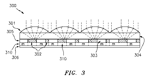
appearance, and the visible binary code.
18
CA 03051841 2019-07-26
WO 2018/147966 PCT/US2018/013348
[0066] The
UV-absorbing component used in the subject invention may be
observable in only the ultraviolet region of the electromagnetic spectrum or
it may be
observable in both the ultraviolet and the visible regions of the
electromagnetic spectrum.
Similar to the IR-absorbing component, the UV-absorbing component may be
present in
a continuous manner or in the form of an intermittent pattern.
[0067] In
one exemplary embodiment, the UV-absorbing component is observable
in only the ultraviolet region of the electromagnetic spectrum and is present
in the form of
a binary code. Two means for authentication are offered by the inventive
optical security
device of this embodiment, namely, the characteristic UV signature and the UV
binary
code.
[0068] In
another exemplary embodiment, the UV-absorbing component is
observable in both the ultraviolet and the visible regions of the
electromagnetic spectrum
and is present in the form of a binary code. Four means for authentication are
offered by
this embodiment, namely, the characteristic UV signature, the UV binary code,
the visible
appearance, and the visible binary code.
[0069] In
yet another exemplary embodiment, a combination of IR-absorbing and
UV-absorbing components are present in the Mr0SD. One or both of these
components
may also be observable in the visible region and may be present in either a
continuous or
intermittent pattern.
[0070] The
Mr0S0 may be used in the form of, for example, a security strip,
thread, patch, or overlay and mounted to a surface of, or partially embedded
within a
fibrous or non-fibrous (e.g., polymer) sheet material (e,g,, banknote,
passport, ID card,
credit card, label), or commercial product (e.g., optical disks, CDs, DVDs,
packages of
medical drugs), etc., for authentication purposes. The inventive device may
also be used
in the form of a standalone product (e,g., substrate for subsequent printing
or
personalization), or in the form of a non-fibrous sheet material for use in
making, for
example, banknotes, passports, and the like, or it may adopt a thicker, more
robust form
for use as, for example, a base platform for an ID card, high value or other
security
document,
[0071] When
used in the form of a security strip, thread, patch, or overlay, the total
thickness of the inventive device is preferably less than about 50 microns
(more
preferably, less than about 45 microns, and most preferably, from about 10 to
about 40
microns).
19
CA 03051841 2019-07-26
WO 2018/147966 PCT/US2018/013348
[0072] The
security strips, threads, patches and overlays may be partially
embedded within or mounted on a surface of a document. For partially embedded
strips
and threads, portions thereof are exposed at the surface of the document at
spaced
intervals along the length of the strip or thread at windows or apertures in
the document.
[0073] The
inventive optical security devices may be at least partially
incorporated in security papers during manufacture by techniques commonly
employed in
the papermaking industry. For example, the inventive security device in the
form of a strip
or thread may be fed into a cylinder mould papemiaking machine, cylinder vat
machine,
or similar machine of known type, resulting in partial embedment of the strip
or thread
within the body of the finished paper.
[0074] The
security strips, threads, patches and overlays may also be adhered or
bonded to a surface of a document with or without the use of an adhesive.
Bonding without
the use of an adhesive may be achieved using, for example, thermal welding
techniques
such as ultrasonic welding, vibration welding, and laser fusing. Adhesives for
adhering
the inventive devices to a surface of a document may be one of hot melt
adhesives, heat
activatable adhesives, water-activated adhesives, pressure sensitive
adhesives, and
polymeric laminating films. These adhesives are preferably crosslinkable in
nature, such
as UV cured acrylic or epoxy, with crosslinking achieved while the adhesive is
in the melt
phase.
[0075]
Suitable documents into which the Mr0SD may be integrated or otherwise
embedded include those of any kind having financial value, such as banknotes
or
currency, bonds, checks, traveler's checks, lottery tickets, postage stamps,
stock
certificates, title deeds and the like, or identity documents, such as
passports, ID cards,
driving licenses and the like, or non-secure documents, such as labels. The
MrOSD is
also contemplated for use with consumer goods as well as bags or packaging
used with
consumer goods.
[0076] In
another contemplated embodiment, the inventive device forms part of a
label construction. The inventive device may be placed on the inside of a
package, so
that the synthetic image(s) remains visible.
[0077] When
used in the form of a base platform for an ID card, high value or other
security document, the total thickness of the inventive device is preferably
less than or
equal to about 1 millimeter (mm) including (but not limited to) thicknesses:
ranging from
CA 03051841 2019-07-26
WO 2018/147966 PCT/US2018/013348
about 200 to about 500 microns; ranging from about 50 to about 199 microns;
and of less
than about 50 microns.
[0078] While various embodiments of the present invention have been
described
above, it should be understood that they have been presented by way of example
only,
and not limitation. Thus, the breadth and scope of the present invention
should not be
limited by any of the exemplary embodiments.
[0079] The invention will be further clarified by reference to certain
specific
drawings reflecting certain specific embodiments of the present invention.
[0080] The Mr-component may be present in a continuous manner or in the
form
of an intermittent pattern. As best shown in FIG. 1, the intermittent pattern
may be in the
form of similar or different size horizontal bars (see FIGS. la, Id, le),
chevrons or zig
zags (see FIG. lc), angled bars (see FIG. lb), shapes, indicia (see FIG. If),
or the like,
or combinations thereof.
[0081] In one embodiment, as illustrated in FIG. 2, the Mr-component
(210) of the
Mr0SD (200) is a patterned layer integrated into the image layer (205), where
the Mr0SD
comprises a focusing layer of focusing elements (201) disposed over the image
layer (205)
of image elements (202) and surrounding solid regions (203), A spacer layer
(204) is
disposed between the focusing elements (201) and the image elements (202).
Here the
image elements are voids partially filled with a contrasting element.
[0082] In a further exemplary embodiment, as depicted in FIG. 3, the Mr-
component (310) of the Mr0SD (300) is a discrete layer disposed between an
image layer
(305) of image elements (302) and an pacifying layer (306). The Mr0SD (300)
comprises
a spacer layer (304) disposed between a focusing layer of focusing elements
(301) and
an image layer (305) of image elements (302) (filled voids) and surrounding
solid regions
(303).
[0083] In another exemplary embodiment, as depicted in FIG. 4, the Mr-
component (410) of the MrOSD (400) is integrated with the Mr0SD as a patterned
layer
disposed between the MrOSID's spacer layer (404) and image layer. Here the
image
elements (402) are protrusions (402), which may be printed onto the spacer
layer (404).
Here the Mr0SD comprises a spacer (404), which is disposed between a focusing
layer
of focusing elements (401) and an array of image elements (402). The Mr0SD
(400) also
includes an additional layer (406) which functions as an adhesive layer.
21
CA 03051841 2019-07-26
WO 2018/147966 PCT/US2018/013348
[0084] In another exemplary embodiment, as depicted in FIG. 5, the Mr0SD
(500)
is as described in FIG. 4. The Mr08D (500) comprises a spacer layer (504),
which is
disposed between a focusing layer of focusing elements (501) and an array of
image
elements (502). Here the Mr-component (510) is integrated into the OSD by
being
distributed in an additional layer (506).
[0085] The Mr0SD, in one embodiment, is illustrated by FIG. 6, wherein
the image
elements (602) of Mr0SD (600) are dollar signs arranged in an array in the
image layer
beneath the spacer layer (604). The spacer layer (604) is disposed between the
image
elements (602) and the focusing layer of focusing elements (601). Here, the Mr-
component (610) is a discrete layer of an 1R-absorber having very little
absorption in the
visible spectral range, but is detectable in the IR spectral range such that
at least two Mr-
signals are detectable in the invisible spectral range.
[0086] A secured product prepared using the Mr0SD of FIG. 6 (marked with
reference number (712)) is exemplified in FIG. 7, Here, the synthetic image
(720) of
Mr0SD (600) projected by the image elements , when viewed through the focusing
elements (601) of FIG. 6, is a dollar sign. The Mr0SD (600) is coupled to a
substrate
(711) of the high security product (700). The high security product (700) is a
banknote
having the Mr0SD (712) coupled to the banknote substrate as a partially
embedded (e.g.,
windowed) thread, where the thread weaves in and out of the paper.
[0087] Presence of an authentic Mr0SD can be confirmed by a signature
detector.
An authentic Mr0SD will indicate a predetermined characteristic Mr-signature.
An
exemplary predetermined characteristic Mr-signature (800) is depicted by FIG.
8, wherein
the top curve indicates a thread, such as an OSD without an Mr-component,
while the
bottom curve indicates a thread, such as an OSD with the Mr-component shown by
the
presence of the characteristic Mr-signature. As noted in the spectrograph of
FIG. 8, the
slope of the Mr-signals in the wavelength range of from 800 to 900 nm
increases when
the Mr-component is missing and decreases when the Mr-component is present as
you
increase the wavelength.
[0088] It should be understood that the Mr-component may alternatively
be
integrated into multiple layers of the OSD. Moreover, it is also contemplated
herein that
the focusing elements are reflective or a combination of refractive and
reflective.
Alternative predetermined Mr-signatures are also contemplated, including
specific
absorption or emission at specific wavelengths.
22
CA 03051841 2019-07-26
WO 2018/147966
PCT/US2018/013348
[0089] What is claimed is:
23