Note : Les descriptions sont présentées dans la langue officielle dans laquelle elles ont été soumises.
High Voltage Start-up Circuit for Switching Power Supplies
Related Application
This application claims the benefit of the filing date of Application No.
62/890,574,
filed on 22 August 2020, the contents of which are incorporated herein by
reference in their
entirety.
Field
This invention relates to start-up circuits for power supplies. More
particularly, the
invention relates to high voltage start-up circuits for switching mode power
supplies.
Background
In switching power supplies a start-up apparatus (i.e., a start-up circuit) is
used to
establish power for the for the primary side control circuit at initial power
up. It is preferred to
automatically disconnect the start-up power circuit during normal operation
when a separate
power source is used to provide the energy/power to the control circuit in
order to achieve less
power consumption. Auto disconnection is a key function in applications where
ultra-low
standby power is required. Fig. 1 shows a typical implementation of a start-up
circuit 10 and
auxiliary power source from a transformer winding Na, according to the prior
art. In this case,
the auxiliary winding Na generates an auxiliary voltage across capacitor Caux
during normal
operation. During the start-up period, the start-up circuit provides voltage
across Caux which is
used, via a regulator 12, to power the control circuit 14. The control circuit
provides gating
signals to the primary side components 16.
Such an arrangement may employ normally-on devices in the start-up circuit,
e.g., a
depletion-mode junction field-effect transistor (JFET). Such devices can
conduct current with no
control voltage applied to the gate. Thus, they are good candidates for start-
up before the control
circuit is powered up. However, available JFETs have a low voltage rating
(below 50V) and low
power rating (below 1W). Accordingly, they are mostly used for low voltage
ICs, but not for
- 1 -
Date Recue/Date Received 2020-08-21
offline AC-DC power supplies, such as power adapters for laptop computers and
cellphones.
Some analog control ICs feature low power consumption, and the supply current
is in
the sub-milliampere (mA) range. Such control circuits may be powered directly
from a high
voltage bus with a startup circuit and low stand-by power consumption.
However, other analog
control ICs and most digital controllers usually require several milliamperes
to hundreds of
milliamperes of supply current. These may require several watts to tens of
watts with high
voltage at hundreds of volts, which is difficult to accommodate and results in
significant stand-
by power consumption.
Summary
One aspect of the invention relates to a start-up circuit for a power
converter,
comprising: an input that receives a power converter primary side DC bus
voltage; a charging
circuit that uses the DC bus voltage to generate a charging current to charge
an energy storage
device to a selected voltage; an auxiliary power output circuit including a
transformer primary
side auxiliary winding; a sensing circuit that senses the primary side DC bus
voltage; and a
control circuit that controls one or more switches of the start-up circuit and
one or more switches
of the power converter primary side, and disables the start-up circuit when
the auxiliary power
output is established; wherein the charging current provides power to the
control circuit until the
auxiliary power is established.
In one embodiment the control circuit comprises a timer; wherein the timer
generates a
signal that disables the start-up circuit after a selected time period;
wherein the auxiliary power
output is established by the end of the selected time period.
In one embodiment the selected time period is about 10 ms to about 1 s.
In one embodiment the selected time period is about 25 ms to about 50 ms.
In one embodiment the control circuit comprises an auxiliary voltage sensor
and the
control circuit generates a signal that disables the start-up circuit when the
sensed auxiliary
voltage is at a selected voltage.
In one embodiment the auxiliary voltage sensor comprises a resistor divider
network
and an analogue-to-digital converter (ADC).
- 2 -
Date Recue/Date Received 2020-08-21
In one embodiment the control circuit comprises a microcontroller unit (MCU).
In one embodiment the start-up circuit comprises a latch circuit that
transfers power
from the energy storage device to the control circuit when the energy storage
device reaches the
selected voltage; wherein the energy storage device provides power to the
control circuit until the
auxiliary power is established.
In one embodiment the energy storage device is a capacitor.
In one embodiment the sensing circuit comprises a resistor-divider network.
In one embodiment the resistor-divider network also provides biasing for a
power
switch of the charging circuit.
A start-up circuit according to the embodiments may be implemented in an AC-DC
power converter. The AC-DC power converter may be a power adapter for a
portable electronic
device.
Another aspect of the invention relates to an AC-DC power converter comprising
a
start-up circuit as described herein.
Another aspect of the invention relates to a method for implementing a start-
up circuit
for a power converter, comprising: using a DC bus voltage of the power
converter to generate a
charging current to charge an energy storage device to a selected voltage;
providing an auxiliary
power output circuit including a transformer primary side auxiliary winding;
using a control
circuit to control one or more switches of the start-up circuit and one or
more switches of the
power converter primary side, and to disable the start-up circuit when the
auxiliary power output
is established; wherein the charging current provides power to the control
circuit until the
auxiliary power is established.
In one embodiment of the method, the control circuit comprises a timer;
wherein the
timer generates a signal that disables the start-up circuit after a selected
time period; wherein the
auxiliary power output is established by the end of the selected time period.
The method may
include setting a time period of about 10 ms to about 1 s, or about 25 ms to
about 50 ms.
In one embodiment of the method, the control circuit comprises an auxiliary
voltage
sensor and the control circuit generates a signal that disables the start-up
circuit when the sensed
auxiliary voltage is at a selected voltage.
- 3 -
Date Recue/Date Received 2020-08-21
In one embodiment the method comprises using a latch circuit to transfer power
from
the energy storage device to the control circuit when the energy storage
device reaches the
selected voltage; wherein the energy storage device provides power to the
control circuit until the
auxiliary power is established.
In one embodiment the method comprises implementing the start-up circuit in an
AC-
DC power converter, wherein the AC-DC power converter may be a power adapter
for a portable
electronic device.
Brief Description of the Drawings
For a greater understanding of the invention, and to show more clearly how it
may be
carried into effect, embodiments will be described, by way of example, with
reference to the
accompanying drawings, wherein:
Fig. 1 is a circuit diagram of a start-up and auxiliary power circuit
according to the prior
art.
Figs. 2A-2D are circuit diagrams of start-up and auxiliary power circuits
according to
various embodiments.
Fig. 3 is a diagram showing voltage waveforms of the embodiment of Fig. 2A
during
start-up.
Detailed Description of Embodiments
Described herein is a start-up apparatus (i.e., start-up circuit) for high
voltage power
converters, used to establish auxiliary power for the power converter primary
side control circuit
at initial power up. In some cases, a start-up circuit embodiment of the
invention may
substantially replace a start-up circuit of a prior designs. For example, in
the prior AC-DC
converter shown in Fig. 1, the start-up circuit 10 may be replaced with a
start-up circuit
according to an embodiment described herein. The AC-DC power converter, also
referred to
herein as a power supply or power adapter, may be, for example, a switching
power converter.
Power adapters may be of the type used to supply power and charge batteries of
portable
- 4 -
Date Recue/Date Received 2020-08-21
electronic devices such as laptop computers, tablets, and cellular phones.
Some embodiments are
suitable for power converters with an AC input from the utility grid, with AC
input voltages of,
e.g., 110-240 VAC. Such power converters may have a primary side DC voltage
bus of, e.g.,
200-400 V, and may be referred to herein as "high voltage". The start-up
circuit only operates at
the initial power up period and does not operate once auxiliary power is
established. This enables
ultra low standby power consumption to meet industry standards.
According to embodiments described herein, the start-up circuit uses an energy
storage
device such as a storage capacitor as a reservoir. The storage capacitor is
charged with a small
current from the high voltage bus and does not release power to the controller
until the reserved
energy/voltage is high enough. The small charging current allows use of low
power rating
components, resulting in reduced cost and footprint.
In one embodiment, the start-up circuit requires only one high-voltage
transistor and
several low-voltage low-power transistors, and does not require JFETs. Most of
the components
in the circuit can be easily integrated into an IC, and implementation with
discrete components is
feasible as well.
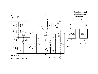
In some embodiments, at least one high voltage switch (e.g., Q1 in Fig. 2A),
one or
more high voltage (and therefore, high value) resistors (e.g., R1 and R2 in
Fig. 2A), and one
energy storage capacitor (e.g., Cl in Fig. 2A) are needed. In some
embodiments, the maximum
voltage across the energy storage capacitor is controlled by a Zener diode
(e.g., Z1 in Fig. 2A).
In order to reduce the power consumption, a start-up control circuit is used
to turn off the high
voltage switch during the normal operating condition of the AC-DC converter,
when the
auxiliary power is established. In some embodiments, the start-up control
circuit may be
implemented with a microcontroller unit (MCU).
In one embodiment, a latch circuit is used to extend the operation range of
the energy
storage capacitor in the start-up circuit (e.g., Cl in Fig. 2A). The capacitor
can be discharged to a
low voltage (e.g., 5V) from its initial voltage (e.g., 25V) so that almost all
the energy stored in
the capacitor can be utilized. This means that a smaller value capacitor is
needed for a fixed time
period required for the start-up of the power supply. In one embodiment, such
as that shown in
Fig. 2A, a Zener diode (Z2), a PNP bipolar junction transistor (BJT) (Q2) and
an N-channel
MOSFET (Q5) are used to implement the latch circuit. By changing the voltage
potential of the
- 5 -
Date Recue/Date Received 2020-08-21
base terminal of Q2, the on and off duration of Q2 can be controlled and
therefore the capacitor
Cl discharging time can be extended. Before Q2 is turned on, its voltage
potential at the base
terminal is high as determined by the Zener diode Z2. When Q2 is turned on,
the Zener diode Z2
is short circuited by turning on of Q5. Q5 is turned on by the voltage across
Cl (Vcl) through
.. the resistor divider (R7, R8). Therefore, the voltage potential of the base
terminal of Q2 is low
and Q2 will remain on even when the voltage across Cl becomes lower. During
normal
operation, Q5 is turned on by the control circuit (an MCU is used as an
example).
In some embodiments a resistor divider network is used to set the biasing of
the main
power switch in the start-up circuit. The same resistors may be used to sense
the converter input
.. voltage (i.e., the DC bus voltage) during normal operation of the power
supply. In addition, in
one embodiment two low voltage switches (e.g., Q3 and Q4 in Fig. 2A) are used
to turn off the
high voltage switch (Q1) and to sense the input voltage. Therefore, the same
high voltage
resistor(s) of the start-up circuit may be utilized during both start-up and
normal operation.
Thus, as described herein, a resistor divider network provides both biasing
for the high
voltage switch of the start-up circuit and a point of monitoring the converter
input voltage during
steady state operation. Since input voltage monitoring is required by most
applications, multi-use
of the resistors helps to reduce the standby power loss and cost.
Operation will now be described in detail with reference to the embodiment of
Fig. 2A.
Referring to Fig. 2A, dashed lines separate different portions of the circuit,
wherein 20, 22, and
.. 24 are the start-up circuit and 26 is an example of an auxiliary power
supply from an auxiliary
transformer winding Na. In cases where the output voltage of the auxiliary
power supply 26 is
too high for the subsequent control circuit, a Buck converter 27 may be used
to provide suitable
power to the control circuit 28, e.g., a microcontroller unit (MCU). As can be
seen in Fig. 2A,
the MCU 28 is used to control operation of the start-up circuit, and to
provide driving signals to
one or more switches of the converter primary side components during normal
operation.
The circuit in 20 is a resistor divider network for monitoring the input
voltage Vbus and
for biasing Ql. R1 and R2 are of large ohmic values (e.g. 1 MegaOhm (Me)) and
200V or
higher voltage rating for 120V and/or 220V AC application. Since Vbus may be a
high voltage,
R1 and R2 are implemented as series resistors (instead of a single resistor)
to improve circuit
.. reliability. Q3 is a P channel MOSFET biased by R5 to be at off state (not
conducting current)
- 6 -
Date Recue/Date Received 2020-08-21
initially. Q4 is an N channel MOSFET controlled by, e.g., the MCU 28 I/O ports
or other control
signals from a controller. After start-up is finished, Q4 is turned on by the
control signal, which
further turns on Q3 by pulling its gate to ground. It is noted that the start-
up operation is
considered finished when the auxiliary winding voltage VNa is established and
provides current
to the control circuit (e.g., the Buck converter 27 and the MCU 28, in the
embodiment of Fig.
2A). Then R5 and R6 are connected in parallel and the voltage across the
parallel connection of
R5 and R6 is proportional to the input voltage (or bus voltage as shown in
Fig. 2A). The relation
of the sensed voltage Vbus sns and the actual bus voltage is shown in (1).
R5 // R6
Vbus sns = * Vbus (1)
¨ R5//R6+R1+R2
The circuit in 22 includes the storage capacitor (reservoir) Cl and its
charging circuit.
As noted above, R1 and R2 in 20 also serve as the biasing resistors for Q1 in
22. Q1 may be
implemented with an NPN BIT. After Vbus is established, the charging current
of Cl (Icl) can
be calculated approximately by (2), if the voltage drop on Q1 and D2 is
neglected.
Vbus ¨Vc1
Id = (2)
R3+R4
Typically, R3 and R4 can dissipate up to 1W at start-up, which means the
charging
current Id l is about 2.5 mA for a 400V bus. As noted above in respect of R1
and R2, R3 and R4
are also implemented as series resistors to improve circuit reliability.
In the case that the controller (e.g., MCU 28) needs lower supply current than
Id, the
circuit shown at 24 can be omitted and the controller can be powered by the
bus directly. Such an
embodiment is shown in Fig. 2B. Cl will be charged to and remain at the
breakdown voltage of
the Zener diode Zl.
However, if the controller requires a higher supply current than Icl, then the
controller
supply voltage cannot be sustained due to overloading. Vcl and Vc2 will remain
very low (e.g.,
2-3 volts). It is noted that in many cases, the charging current Id l is lower
than the supply current
required by the controller.
To accommodate a high supply current of the controller, the circuit in 24
(Fig. 2A) is
used for holding and releasing the power stored in Cl. Q2 (e.g., a PNP BIT or
a P-channel
MOSFET) is at off state initially, so Cl will not be discharged through Q2 and
Cl is charged by
- 7 -
Date Recue/Date Received 2020-08-21
the Vbus with a small current as shown in equation (1). After Cl voltage
reaches the breakdown
voltage of Z2, Q2 is turned on. The voltage at the collector of Q2 becomes
high and the voltage
at the gate of Q5 is high also through resistors R7 and R8. Therefore, Q5 is
turned on
automatically when Q2 is turned on. After Q5 is turned on, the base voltage of
Q2 becomes low
and Z2 is shorted to ground. Then, Q2 will continuously conduct current as
long as Vcl is
positive.
For a typical design, the breakdown voltage of Z1 (Vzl) is about 25V and the
breakdown voltage of Z2 (Vz2) is about 22V. Only limited energy stored in Cl
can be released.
That is, Q2 will conduct for a much shorter period of time. It is noted that
the energy stored in a
capacitor is proportional to the capacitor value and the square of the
capacitor voltage.
With the circuit in 24, Q2 will remain on when Vcl is from about 25V to about
5V.
Therefore, most of the energy stored in Cl will be released and Q2 will
conduct for a much
longer time. While Q2 is on, Cl will provide the power to C2 and the next
stage circuit with
adequate supplying current. Therefore, the circuit in 24 (Q2, Q5, and Z2, and
related
components) serves as a latch circuit to keep Q2 on so that Cl can be
discharged to a low
voltage.
After the power from the auxiliary winding Na is established, the MCU 28 will
produce
a signal to turn on Q4 through the I/O port, then the circuit in 20 will
monitor the input voltage.
The sensing point voltage is below about 3.3V, and it is lower than the
voltage on Cl. Thus, Q1
is automatically turned off after Q4 is turned on.
As described above, the start-up operation is considered finished when the
auxiliary
winding voltage VNa is established and provides current to the control circuit
(e.g., the MCU 28,
and optionally the Buck converter 27 in the embodiments of Figs. 2A and 2B).
Two ways of
controlling switching of the power source from the start-up circuit (20, 22,
and optionally 24 in
Fig. 2A) to the auxiliary power circuit (26 in Fig. 2A) are described below.
Once the MCU is powered up from the start-up circuit (i.e., Cl), the MCU
starts a timer
of, e.g., 10 ms to 1 s, typically about 25 ms to 50 ms. After this delay, the
MCU will turn off the
start-up circuit by sending a control signal to turn on Q4 (and, when the
latch circuit 24 is used,
also sending a control signal to turn on Q5). Then the auxiliary power circuit
26 will provide
power for MCU. The design of the Cl value, Z1 breakdown voltage, and the delay
time ensures
- 8 -
Date Recue/Date Received 2020-08-21
auxiliary power is established by the time the start-up circuit is turned off.
Alternatively, once the MCU is powered up from the startup circuit (i.e., Cl),
the MCU
senses the auxiliary voltage Vaux through sensing resistors, e.g., R9 and R10
as shown in the
embodiments of Figs. 2C and 2D. When Vaux reaches a selected level, the MCU
will shut down
the start-up circuit by sending a control signal to turn on Q4 (and, when the
latch circuit 24 is
used, also sending a control signal to turn on Q5). Then the auxiliary power
circuit 26 will
provide power for MCU.
It is noted that the auxiliary winding Na is one way to provide power to the
control
circuit during normal operation. Another way to provide power to the control
circuit is to use a
DC to DC converter from the secondary side (i.e., the output side) of the AC-
DC converter.
It should be noted that in the embodiments shown in Figs. 2A, 2B, 2C, and 2D,
all
MOSFETs can be replaced by BITs and vice versa.
Fig. 3 shows the voltage waveforms during start-up. Vac is the AC voltage from
the
utility grid. Vbus is the voltage after rectifiers. At to, the converter is
connected to the AC outlet,
and Vbus increases to the peak of the AC voltage. In the meantime, Cl is
slowly charged by
Vbus. At ti, Vcl reaches the breakdown voltage of Z2 at Vz2. Then T2 is turned
on and Cl
releases power to C2. The MCU starts to operate at ti. After ti, the energy
stored in Cl will be
released through Q2 to provide power (energy) for operation of the control
circuit, such as the
Buck converter 27 and MCU 28, as shown in Fig. 2A. At t2, the main power
converter starts to
operate and the auxiliary voltage from the winding starts to build up. Once
the auxiliary voltage
is established at t3, Q5 is turned off by a control signal from the MCU 28.
Then Q1 will be off
and Q2 will also be off. No current will flow through Ql. The control circuit
(e.g., Buck
converter 27 and MCU 28) will be powered only by the auxiliary winding Na. Q4
can be turned
on at any time after ti. When Q4 is turned on, Q3 will also be turned on and
the base voltage of
Q1 will be low (below 3.3V, for example).
Equivalents
While the invention has been described with respect to illustrative
embodiments thereof,
it will be understood that various changes may be made to the embodiments
without departing
- 9 -
Date Recue/Date Received 2020-08-21
from the scope of the invention. Accordingly, the described embodiments are to
be considered
merely exemplary and the invention is not to be limited thereby.
- 10 -
Date Recue/Date Received 2020-08-21