Note : Les descriptions sont présentées dans la langue officielle dans laquelle elles ont été soumises.
Graphitic room-temperature superconductor
TECHNICAL FIELD
The disclosure relates to a high (critical) temperature superconductor, in
particular a graphite-
based high (critical) temperature superconductor making use of wrinkles in the
topmost layers
of graphite near a surface or an interface.
BACKGROUND
Superconductivity is a phenomenon observed in materials characterized by the
zero-
resistance, i.e., vanishing electrical resistance state of a material, and by
expulsion of the
magnetic field from the material. Materials exhibiting these properties are
called
superconductors. In practical experiments, superconductivity is ordinarily
identified as a
dissipationless (i.e., loss-free, i. e., with much lower energy losses related
to current transport
than in conventional, non-superconducting materials) current through the
material. The
phenomenon was discovered in 1911 for mercury (Hg), which becomes
superconducting below
its superconducting transition temperature (Tc) of 4.2K, also referred to as
critical
temperature. Below Tc, mercury exhibits superconductivity, above Tc it behaves
like a
conventional material with the conventional resistivity of mercury. In
experiments, when the
superconducting material is heated from a temperature below Tc to a
temperature above Tc,
its resistance jumps from zero to a finite (i. e., much larger) value at the
superconducting
transition temperature Tc. Ever since this discovery, the tireless search for
materials exhibiting
superconductivity at higher and elevated Tc has never stopped.
Superconductivity in materials with critical temperatures exceeding 20 K is
referred to as high
(critical) temperature superconductivity (HTC). The discovery of HTC in Ba-La-
Cu-O cuprates
with Tc ¨ 30 K (see J. G. Bednorz and K. A. Muller, Z. Phys. B 64, 189 (1986))
and Y-Ba-Cu-O
with Tc as high as 93 K (see M. K. Wu et al., Phys. Rev. Lett. 58, 908 (1987))
made
superconductivity at ambient conditions (280 K to 310 K, 1o5 Pa), also
referred to as "Room
Temperature Superconductivity" (RTS), seem possible, and triggered a race for
the
development of a material to show RTS. So far, the highest Tc =135 K at
ambient pressure has
been achieved for HgBa2Ca2Cu309 (see A. Schilling et al., Nature 363, 56
(1993)), and Tc was
raised up to 164 K under pressure of 30 GPa (see L. Gao et al., Phys. Rev. B
50, 4260 (1994)).
1
Date Recue/Date Received 2023-03-07
Outside of cuprates, the bulk superconductivity with highest Tc = 33 K at
ambient pressure has
been observed in CsxRbyC6o (see K. Tanigald, Nature 352, 222 (1991)), an
alkali-doped
Buckminster fullerene.
Very recently, the zero-resistance state near room temperature has been
reported for various
hydride systems under pressure P> 200 GPa (for a review article, see G. Gao et
al, Materials
Today Physics 100546 (2021), in press).
Graphite is another promising material in a race for RTS. First, bulk
superconductivity was
found in the alkali-metal graphite intercalation compound C8K with a
superconducting
transition temperature Tc = 0.15 K (see N. B. Hannay et al., Phys. Rev. Lett.
14, 225 (1965)),
.. and 40 years later in C6Yb with Tc = 6.5 K (see T. E. Weller, et al.,
Nature Physics 1, 39 (2005))
and C6Ca with Tc = 11.5 K (see N. Emery et al., Phys. Rev. Lett. 95, 087003
(2005)).
OVERVIEW
In view of the technical problems laid out above, there is a need for a
superconductor with a
superconducting transition temperature (critical temperature; Tc) of at least
room
temperature (280 K to 310 K), preferably at ambient pressure (o .o 8 to 0.12
MPa). In the
context of this disclosure, the term superconductor refers to a device adapted
to transport an
essentially dissipationless electrical current (in other word, exhibits a zero-
resistance state or
a vanishing (electrical) resistance state, respectively). The essentially
dissipationless electrical
current may be characterized by a resistance or resistivity at least a hundred
times smaller than
a resistance or resistivity of a similar device (e. g., with a similar or
identical material
composition, in particular the same device) in a non-superconducting state (e.
g. above a
critical temperature and/or not exhibiting all the structural features of the
claimed subject-
matter).
This objective is achieved with a superconductor device according to claim 1.
Claim 14 provides
a use of a graphite structure as a superconductor device. Claim 15 refers to a
method for
fabricating a superconductor device. The dependent claims relate to preferred
embodiments.
In a first aspect, a superconductor device comprises a graphite structure, a
first electrode, a
second electrode, and a wrinkle region. The graphite structure comprises at
least one topmost
atomic layer. The first electrode is arranged over the at least one topmost
atomic layer. The
second electrode is arranged over the at least one topmost atomic layer and
spaced apart from
the first electrode. The wrinkle region is comprised in the at least one
topmost atomic layer.
The wrinkle region is arranged between the first electrode and the second
electrode and
comprises a plurality of wrinkles comprising a pair of wrinkles. The first
electrode and the
second electrode both electrically contact both wrinkles of the pair. A
distance between the
wrinkles of the pair is at most 0.2 gm.
2
Date Recue/Date Received 2023-03-07
This superconductor device may exhibit a zero-resistance state at room
temperature and
above, and at ambient pressure. The zero-resistance state may be considered
characteristic for
superconductivity and, within the context of this disclosure, the defining
feature of
superconductivity. The zero-resistance state of the superconductor device has
been
.. demonstrated and proven in various experiments, which will be described in
detail throughout
this disclosure. The superconductor device may therefore implement the long
sought after
room-temperature superconductor. The zero-resistance state may open a plethora
of
application examples, for example related to quantum computing using the room-
temperature
superconductor or dissipationless current and information transport in
otherwise
conventional electronic devices such as integrated semiconductor electronics.
The zero-resistance state (and thus the
superconductor/superconductivity/superconductor
device according to the disclosure) may be distinguished from local
(microscopic)
superconductivity, which is implemented in materials that show some of the
characteristics
which are conventionally related to superconductivity, but not the zero-
resistance state.
Results of earlier experiments may be related to local, microscopic
superconductivity in small
volume fractions of graphite at temperatures as high as 300 K (see, e. g., Y.
Kopelevich et al.,
J. Low Temp. Phys. 119, 691 (2000); R. R. da Silva et al. Phys. Rev. Lett. 87,
14700 (2001); N.
P. Yang et al., Chin. Phys. Lett. 18, 1648 (2001); S. Moehlecke et al., Phil.
Mag. B 82, 1335
(2002); Y. Kawashima, MP Advances 3, 052132 (2013); Y. Kopelevich et al.,
Physica C 514, 237
(2015)). In particular, several decades ago, Antonowicz measured Josephson-
type oscillations
and Shapiro-like steps in I-V characteristics at room temperature in Al-AC-Al
sandwiches (AC
= amorphous carbon) (cf. K. Antonowicz, Nature 247, 358(1974); Phys. Status
Solidi A 28,497
(1975)). To go into the details of some of the other examples, magnetization
measurements of
both sulfur (S)-doped AC (see I. Felner et al., Phys. Rev. B 79, 233409
(2009)) and S-doped
graphite (R. R. da Silva et al. Phys. Rev. Lett. 87, 14700 (2001); N. P. Yang
et al., Chin. Phys.
Lett. 18, 1648 (2001); S. Moehlecke et al., Phil. Mag. B 82, 1335 (2002)) have
pointed towards
the local superconductivity with nearly the same highest Tc of ¨ 38 K. Because
AC consists of
curved graphene and/or fullerene-like fragments (see P. J. F. Harris et al.,
Phil. Mag. Lett. 8o,
381 (2000)), one assumes that similar structural defects in graphite might be
responsible for
the high-temperature local superconductivity. So far, the efforts to achieve a
zero-resistance
state in graphite have failed (see e. g. A. Ballestar et al., Carbon 72, 312
(2014); P. D. Esquinazi
et al., Quantum Stud.: Math. Found. 5, 41 (2018)).
The zero-resistance state of the superconductor device, also referred to as
global
superconductivity in the context of this disclosure, may be related to current
transport along
the direction of continuous, electronically coupled wrinkles in the topmost
layers of the
graphite. The electronic coupling may be ensured by using wrinkles with a
spacing (distance)
3
Date Recue/Date Received 2023-03-07
within a critical value of around 0.2 gm. To induce and pick off a
superconducting current
through the electronically coupled wrinkles, the (very same) wrinkles may be
contacted at
different positions using the electrodes. This arrangement may be considered
the key to the
implementation of the superconductor device.
The distance between the wrinkles of the pair may refer to a minimum distance
between the
wrinkles of the pair.
Alternatively, or in addition, the distance between the wrinkles of the pair
may refer to an
average distance between the wrinkles of the pair.
Alternatively, or in addition, the distance between the wrinkles of the pair
may refer to a
maximum distance between the wrinkles of the pair.
The distance between the wrinkles of the pair may be at most 0.15 gm, in
particular at most
0.1 f1M.
Alternatively, or in addition, each wrinkle of the plurality may comprise an
average distance to
its respective neighboring wrinkle. A mean wrinkle distance may be defined by
a mean of the
average distances of all wrinkles of the plurality. The mean wrinkle distance
may be at most
0.2 gm, in particular at most 0.15 gm or at most 0.1 gm.
The wrinkles of the pair may be neighboring wrinkles. In particular, the
(minimum) distance
between the wrinkles of the pair may be no larger than a second wrinkle
distance between any
wrinkle of the pair and any other wrinkle.
The wrinkles of the pair may form a branching and/or an intersection. In
particular, at least
ten wrinkles of the plurality of wrinkles and respective neighboring wrinkles
may form
branchings and/or intersections. In particular, at least a quarter of the
wrinkles of the plurality
of wrinkles and respective neighboring wrinkles may form branchings and/or
intersections or
all wrinkles of the plurality of wrinkles and respective neighboring wrinkles
may form
branchings and/or intersections.
Branchings and/or intersections may beneficially enhance the electronic
coupling between the
wrinkles and enhance the critical temperature of the superconductor device.
For an
enhancement, not all wrinkles may need to branch or intersect, even branchings
or
intersections of a minor fraction of the wrinkles may be beneficial.
The superconductor device may be adapted to support a superconducting and/or
essentially
dissipationless current between the first electrode and the second electrode.
In particular, the
superconductor device may be adapted to support the superconducting and/or
essentially
dissipationless current between the first electrode and the second electrode
through the
wrinkle region.
4
Date Recue/Date Received 2023-03-07
The superconductor device may be adapted to support a superconducting and/or
an essentially
dissipationless current between the first electrode and the second electrode
at a temperature
of the wrinkle region of at least 100 K, in particular of at least 140 K, in
particular of at least
18o K, in particular of at least 220 K, in particular of at least 260 K, in
particular of at least 300
K, in particular of at least 300 K or at room temperature.
The superconducting and/or essentially dissipationless current may refer to a
current between
the first electrode and the second electrode, in particular through the
wrinkle region, with a
resistivity at least ten times lower than the bulk resistivity of graphite, in
particular at least 20
times lower than the bulk resistivity of graphite, in particular at least 30
times lower than the
bulk resistivity of graphite or at least 50 times lower than the bulk
resistivity of graphite, in
particular at least 100 times lower than the bulk resistivity of graphite, in
particular at least
500 times lower than the bulk resistivity of graphite, in particular at least
1000 times lower
than the bulk resistivity of graphite or at least 5000 times lower than the
bulk resistivity of
graphite, for example lower than 1 gl/meter at room temperature or lower than
0.1 Cl/meter
at room temperature.
The bulk resistivity of graphite may refer to a resistivity of pure graphite,
in particular, to a
resistivity of graphite comprising less than 3% (in terms of atomic number)
metallic
intercalates such as alkali metal intercalates.
The room temperature may refer to a temperature in a range from 280 K to 310
K.
The superconductor device may be adapted to support, with the wrinkle region
at room
temperature, a current between the first electrode and the second electrode
through the
wrinkle region with a resistivity at least a hundred times lower than the bulk
resistivity of
graphite.
The wrinkle region may be adapted to support at room temperature a current
density between
the first electrode and the second electrode through the wrinkle region of at
least 106 A/cm2
when a voltage between the first electrode and the second electrode is at most
10 nV. In
particular, the current density between the first electrode and the second
electrode through the
wrinkle region may be at least 106 RA/cm2, in particular at least 107 A/cm2.
The wrinkles of the pair may comprise parallel sections.
The parallel sections may correspond to sections of a minimum distance between
the wrinkles
of the pair.
The parallel sections may extend along at least 20% of the respective
extensions of the wrinkles
of the pair between the first electrode and the second electrode, in
particular, along at least
40% of the respective extensions, in particular along at least 6o% of the
respective extensions,
5
Date Recue/Date Received 2023-03-07
in particular along at least 8o% of the respective extensions or along the
entire respective
extensions.
Parallel sections of the wrinkles may beneficially enhance their electronic
coupling, and thus
increase the critical temperature of the superconductor device.
The graphite structure may comprise or be composed of graphite comprising
atomic layers.
The atomic layers may comprise the at least one topmost atomic layer.
Each atomic layer of the plurality of atomic layers may be a layer of carbon
atoms. In particular,
each atomic layer of the plurality of atomic layers may correspond to a
graphene layer.
A ratio between a resistivity of the graphite along a direction perpendicular
to the atomic layers
and the resistivity along the atomic layers may be at least 20000, in
particular at least 25000,
in particular at least 50000 or at least 100000. The resistivity of the
graphite along the
direction perpendicular to the atomic layers may refer to a temperature of the
graphite of
300 K. The resistivity of the graphite along the direction perpendicular to
the atomic layers
and the resistivity of the graphite along the atomic layers may refer to a
section of the graphite
without a continuous wrinkle region or without any wrinkle region.
The graphite structure may comprise at least one bulk atomic layer below the
at least one
topmost atomic layer. The at least one bulk atomic layer may be comprised in
the plurality of
atomic layers.
In particular, the at least one bulk atomic layer may comprise at least two
bulk atomic layers,
in particular at least three bulk atomic layers, in particular at least four
bulk atomic layers, in
particular at least five bulk atomic layers, in particular at least six bulk
atomic layers, in
particular at least eight bulk atomic layers, in particular at least 10 bulk
atomic layers, in
particular at least 20 bulk atomic layers or at least 50 atomic layers.
Experiments suggest that the electronic coupling may be mediated by bulk
atomic layers below
the topmost atomic layers. Therefore, the bulk atomic layers may beneficially
enhance the
critical temperature of the superconductor device. In particular, the use of
bulk atomic layers
(or a bulk graphite, respectively) of a certain quality may beneficially
enhance the critical
temperature of the superconductor device. The ratio between the resistivity of
the graphite
along the direction perpendicular to the atomic layers and the resistivity
along the atomic
layers may be considered a straightforward characteristic of the quality of
the bulk atomic
layers (or the bulk graphite, respectively).
The at least one topmost atomic layer may comprise at least two atomic layers,
in particular at
least three atomic layers, in particular at least four atomic layers, in
particular at least five
atomic layers, in particular at least six atomic layers, in particular at
least seven atomic layers,
6
Date Recue/Date Received 2023-03-07
in particular at least eight atomic layers, in particular at least nine atomic
layers, in particular
at least 10 atomic layers, in particular at least 100 atomic layers or at
least 1000 atomic layers.
Each bulk atomic layer may comprise a c-axis perpendicular to the bulk atomic
layer.
The c-axis of all bulk atomic layers may be aligned, for example within 30, in
particular within
2 , in particular within 1 , in particular within 0.5 , in particular within
0.3 or within 0.2 .
Experiments indicate that the alignment of the c -axis of the bulk atomic
layers may be
considered another characteristic of the quality of the bulk atomic layers (or
the bulk graphite,
respectively).
The graphite may comprise or be highly oriented pyrolytic graphite.
At least a section of the graphite structure may comprise a Bernal stacking.
In particular, at
least a section of the at least one topmost atomic layer may comprise a Bernal
stacking. In
particular, at least a section of the at least one topmost atomic layer in a
region between the
wrinkles of the plurality of wrinkles may comprise a Bernal stacking.
Alternatively, or in
addition, the at least one bulk atomic layer may comprise a Bernal stacking.
At least a section of the graphite structure may comprise a rhombohedral
stacking. In
particular, at least a section of the at least one topmost atomic layer may
comprise a
rhombohedral stacking.
At least one wrinkle of the plurality of wrinkles may comprise a section with
the rhombohedral
stacking, and optionally a section with the Bernal stacking. In particular, a
majority of the
wrinkles of the plurality of wrinkles or all wrinkles may each comprise a
section with the
rhombohedral stacking, and optionally a section with the Bernal stacking.
A change in the stacking of the atomic layers at/in the wrinkles may be
considered one of the
origins of a superconductivity arising from the wrinkles, which may be at the
origin of the zero-
resistance state.
The at least one topmost atomic layer may comprise at least one flat section,
for example
between at least one pair of wrinkles of the plurality of wrinkles or between
any pair of wrinkles
of the plurality of wrinkles. In particular, the at least one flat section may
comprise or be a or
any section in the wrinkle region with a surface corrugation smaller than an
average surface
corrugation related to the wrinkles and/or with a curvature smaller than an
average maximum
curvature of the wrinkles. For example, the at least one flat section may
comprise a surface
corrugation of at most 3 nm, in particular at most 1 nm or at most 0.5 nm.
The term surface may refer to an interface of the graphite to vacuum, a gas
(such as air), a
liquid (such as an electrolyte), or to another solid.
7
Date Recue/Date Received 2023-03-07
Each layer of the at least one topmost atomic layer in the at least one flat
section may comprise
a c-axis perpendicular to the flat section. The c-axis of all layers of the at
least one topmost
atomic layer in the at least one flat section may be aligned, for example
within 30, in particular
within 2 , in particular within 1 or within 0.5 .
The at least one flat section may define a surface. For example, the surface
may be parallel to
or defined by a plane wherein the at least one flat section extends. In
embodiments, wherein
the at least one flat section comprises at least three flat sections, the
surface may alternatively,
or in addition, be defined as a surface connecting the at least three flat
sections.
Any wrinkle of the plurality of wrinkles may comprise an elongated shape.
The wrinkles of the pair(s) or the wrinkles of the plurality of wrinkles may
comprise or be a
curved section of the at least one topmost atomic layer. In particular, the
curved section of the
at least one topmost atomic layer may be curved out of the surface and/or out
of the flat section.
The wrinkles of the pair(s) or the wrinkles of the plurality of wrinkles may
comprise or be a
fold of the at least one topmost atomic layer. In particular, the fold of the
at least one topmost
atomic layer may be a fold out of the surface and/or out of the flat section.
The wrinkles of the pair(s) or the wrinkles of the plurality of wrinkles may
comprise or be a
protrusion of the at least one topmost atomic layer from the at least one flat
section. In
particular, the protrusion may be a protrusion out of the surface and/or out
of the flat section.
The at least one flat section may comprise a first flat section and a second
flat section. Any
wrinkle of the plurality of wrinkles may refer to a curved section of the at
least one topmost
atomic layer between the first flat section and the second flat section and/or
to a fold of the at
least one topmost atomic layer between the first flat section and the second
flat section and/or
to a protrusion of the at least one topmost atomic layer between the first
flat section and the
second flat section.
The wrinkles of the pair may have the distance of at most 0.2 gm along a
majority of their
respective lengths between the first electrode and the second electrode.
A wrinkle of the pair may comprise a straight segment or the wrinkles of the
pair may comprise
respective straight segments.
The straight segment(s) may extend along at least 30% of a length(s) of the
wrinkle(s) between
the first electrode and the second electrode, in particular along at least 5o%
of the length(s) of
the wrinkle(s), in particular along at least 70% of the length(s) of the
wrinkle(s), in particular
along at least 90% of the length(s) of the wrinkle(s) or along the entire
length(s) of the
wrinkle(s).
8
Date Recue/Date Received 2023-03-07
The straight segment(s) may extend along a direction of the respective
straight segment. The
direction of the straight segment(s) may be perpendicular to the first edge
and/or
perpendicular to the second edge. The direction of the straight segment(s) may
be parallel to
the surface.
The straight segments of the wrinkles of the pair may comprise or be the
parallel sections.
The distance between the wrinkles of the pair may refer to a distance between
the parallel
sections of the wrinkles of the pair, in particular between parallel straight
segments of the
wrinkles of the pair.
The wrinkles of the pair or the parallel sections of the wrinkles of the pair
may have a length of
at least 0.05 mm, in particular at least 0.1 mm, in particular at least 0.2
mm, in particular at
least 0.3 mm or at least 0.4 mm, in particular within the wrinkle region.
The width of the wrinkle region may refer to a minimum extension of the
wrinkle region along
a direction perpendicular to a direction connecting the first electrode and
the second electrode.
Alternatively, the width of the wrinkle region may refer to an average
extension of the wrinkle
region along a direction perpendicular to the direction connecting the first
electrode and the
second electrode.
The first electrode may have a first edge defining a section of a boundary of
the wrinkle region.
The second electrode may have a second edge defining a second section of the
boundary of the
wrinkle region. The second edge may be parallel to or concentric with the
first edge.
The width of the wrinkle region may refer to an extension of the wrinkle
region along a
direction parallel to or concentric with the first edge or the second edge. In
particular, the width
of the wrinkle region may refer to a minimum extension or an average extension
of the wrinkle
region along a direction parallel to the first edge or the second edge.
The first electrode and/or the second electrode may be in direct physical
contact with the at
least one topmost atomic layer, in particular directly above the at least one
topmost atomic
layer. In particular, the first electrode and/or the second electrode may be
in direct physical
contact with the wrinkles of the pair.
The second electrode may be displaced with respect to the first electrode
along the at least one
topmost atomic layer. The second electrode may be at a same height or at a
different height as
the first electrode along a vertical direction perpendicular to the at least
one topmost atomic
layer and/or to the surface.
A wrinkle of the pair or both wrinkles of the pair may extend along a first
wrinkle direction in
a vicinity of the first electrode and/or at its (their) respective contact(s)
to the first electrode.
9
Date Recue/Date Received 2023-03-07
In particular, the wrinkle(s) may be essentially straight along the first
wrinkle direction in the
vicinity of the first electrode. The geometry wherein the wrinkles encounter
the edge of the
electrode(s) at a 90 angle (perpendicularly) may be beneficial for driving a
superconducting/dissipationless current through the superconductor device as
well as for
picking off the superconducting/dissipationless current.
The first edge may be perpendicular to the first wrinkle direction. The first
electrode may
contact a wrinkle with an angle of essentially 90 between the first edge and
the first wrinkle
direction, in particular contact at least 20% of the wrinkles of the plurality
of wrinkles, in
particular at least 30% of the wrinkles, in particular at least 40% of the
wrinkles or at least 50%
of the wrinkles with the angle of essentially 90 between the first edge and
the first wrinkle
direction.
A wrinkle of the pair or both wrinkles of the pair may extend along a second
wrinkle direction
in a vicinity of the second electrode and/or at its (their) respective
contact(s) to the second
electrode(s). In particular, the wrinkle may be essentially straight along the
second wrinkle
direction in the vicinity of the first electrode.
The wrinkles of the pair may extend along the second wrinkle direction in the
vicinity of the
second electrode.
The second edge may be perpendicular to the second wrinkle direction.
A length of the wrinkle region between the first electrode and the second
electrode may be at
least 0.5 gm, in particular at least 1 gm, in particular at least 0.01 mm, in
particular at least
0.05 mm, in particular at least 0.1 mm, in particular at least 0.2 mm, in
particular at least
1 mm, in particular at least 10 mm, in particular at least 100 mm or at least
200 mm.
A width of the wrinkle region may be at least 1 gm, in particular at least 2
gm or at least 50 gm.
The plurality of wrinkles may comprise at least 3 wrinkles, in particular at
least 4 wrinkles, in
.. particular at least 5 wrinkles, in particular at least 10 wrinkles, in
particular at least 100
wrinkles or at least 1000 wrinkles.
The plurality of wrinkles may comprise a dense wrinkle array with at least one
wrinkle.
The plurality of wrinkles may comprise a neighboring wrinkle and an opposite
neighboring
wrinkle of the at least one wrinkle of the dense wrinkle array on its opposite
sides, wherein a
distance between the at least one wrinkle and the neighboring wrinkle and a
distance between
the at least one wrinkle and the opposite neighboring wrinkle may both be at
most 0.2 gm.
The dense wrinkle array may maximize the electronic coupling, thus enhancing
the critical
temperature of the superconductor device, as every densely-packed wrinkle may
be coupled to
Date Recue/Date Received 2023-03-07
at least two neighboring wrinkles on its opposite sides. In particular, the
dense wrinkle array
(densely-packed wrinkles) is free of major sections of the wrinkle region
without wrinkles,
which may not contribute to the dissipationless current.
The at least one wrinkle, the neighboring wrinkle and/or the opposite
neighboring wrinkle may
be characterized by features disclosed above in the context of the wrinkle.
The distance between the at least one wrinkle and the (opposite) neighboring
wrinkle may be
characterized by features disclosed above in the context of the distance
between the wrinkles
of the pair.
The dense wrinkle array may comprise at least two wrinkles, in particular at
least three
wrinkles, in particular at least four wrinkles, in particular at least five
wrinkles, in particular at
least six wrinkles, in particular at least seven wrinkles or at least eight
wrinkles characterized
by the features described above in the context of the at least one wrinkle.
The neighboring wrinkle or the opposite neighboring wrinkle may be a wrinkle
of the dense
wrinkle array.
The dense wrinkle array may be continuous and/or not comprise any flat section
with a width
exceeding 0.2 gm.
A minimum distance between any wrinkle of the dense wrinkle array and any
nearest-neighbor
wrinkle of the dense wrinkle array may not exceed 0.2 gm (for both (reference)
sides of the
wrinkle). The nearest-neighbor wrinkle may be a wrinkle of the dense wrinkle
array on a
reference side of the wrinkle with a minimum distance to the wrinkle smaller
than a minimum
distance between the wrinkle and any other wrinkle of the dense wrinkle array
on the reference
side of the wrinkle.
The at least one topmost atomic layer and/or the plurality of wrinkles may
comprise at least
two dense wrinkle arrays, in particular at least three dense wrinkle arrays,
in particular at least
five dense wrinkle arrays, in particular at least 10 dense wrinkle arrays or
at least 100 dense
wrinkle arrays.
At least a section of the wrinkles of the pair and/or of the wrinkles of the
dense wrinkle array(s)
or of the wrinkles of the plurality may be oriented along a common wrinkle
direction. Having
the wrinkles (at least partially) oriented along the same, common wrinkle
direction may further
improve the parallelism of the wrinkles and thus the electronic coupling
between the wrinkles
and ultimately the critical temperature of the superconductor device.
In particular, the wrinkles of the pair and/or the wrinkles of the dense
wrinkle array(s) or the
wrinkles of the plurality may be oriented along the common wrinkle direction
along the
majority of their respective extensions between the first electrode and the
second electrode. In
11
Date Recue/Date Received 2023-03-07
particular, the wrinkles of the pair and/or the wrinkles of the dense wrinkle
array or the
wrinkles of the plurality may be oriented along the common wrinkle direction
along their
respective entire extensions between the first electrode and the second
electrode.
The common wrinkle direction may be parallel to or coincide with a line
connecting the first
electrode and the second electrode.
The common wrinkle direction may be perpendicular to a direction of the width
of the wrinkle
region and/or to the first edge and/or to the second edge.
The at least section of the wrinkle(s) oriented along the common wrinkle
direction may be a
straight segment of the wrinkle(s), in particular with one or all the features
disclosed above in
the context of the straight segment.
The wrinkles of the pair and/or the wrinkles of the dense wrinkle array(s) may
extend through
all atomic layers of the at least one topmost atomic layer. The at least one
topmost atomic layer
may comprise at least three topmost atomic layers.
The graphite structure may further comprise at least two bulk atomic layers
below the at least
one topmost atomic layer with a bulk layer spacing between neighboring bulk
atomic layers;
and a wrinkle layer spacing between an atomic layer of the at least one
topmost atomic layer
and a neighboring layer of the at least one topmost atomic layer in a wrinkle.
The wrinkle layer
spacing may exceed the bulk layer spacing, in particular by at least 0.5%, in
particular by at
least 1% or at least 1.5%.
A change in the layer spacing of the atomic layers at/in the wrinkles may be
considered one of
the origins of a superconductivity arising from the wrinkles, which may be at
the origin of the
zero-resistance state.
The bulk layer spacing may refer to an average of spacings between neighboring
bulk atomic
layers of the at least two bulk atomic layers.
For example, the bulk layer spacing may be 0.335 nm.
The wrinkle layer spacing may be at least 0.336 nm, in particular at least
0.337 nm or 0.34 nm.
Alternatively, or in addition, the wrinkle layer spacing may be at most 0.344
nm.
The at least two bulk atomic layers may be essentially flat.
In particular, the at least two bulk atomic layers may comprise a corrugation
significantly
smaller than a corrugation of the at least one topmost atomic layer.
A downward vertical extension of the wrinkles of the pair or of a majority of
wrinkles of the
dense wrinkle array(s) or of a majority of wrinkles of the plurality of
wrinkles, may end within
the at least one topmost atomic layer.
12
Date Recue/Date Received 2023-03-07
The majority of wrinkles may refer to at least half of the wrinkles of the
plurality of wrinkles.
A ratio between a height and a width of the wrinkles of the pair and/or of the
wrinkles of the
dense wrinkle array may be at least 0.5, in particular at least 0.7, in
particular at least 0.9, in
particular at least 1.1 or at least 1.3.
The higher the ratio between the height and the width of the wrinkle, the
higher may be its
contribution to the dissipationless current and/or the superconductivity.
A height of the wrinkles of the pair and/or of the wrinkle(s) of the dense
wrinkle array may be
at most 10 nm, in particular at most 8 nm, in particular at most 6 nm, or at
most 2 nm or at
most 1 nm.
An average height of the wrinkles of the pair and/or of the wrinkles of the
dense wrinkle array
may be at most 10 nm, in particular at most 8 nm, in particular at most 6 nm,
or at most 2 nm
or at most 1 nm.
A height of the wrinkles of the pair and/or of the wrinkles of the dense
wrinkle array may be at
least 0.7 nm, in particular at least 1 nm, in particular at least 2 nm or at
least 3 nm.
An average height of the wrinkles of the pair and/or of the wrinkles of the
dense wrinkle array
may be at least 1 nm, in particular at least 2 nm or at least 3 nm.
A width of the wrinkles of the pair and/or of the wrinkles of the dense
wrinkle array may be at
least 0.5 nm, in particular at least 1 nm or at least 1.5 nm.
An average width of the wrinkles of the pair and/or of the wrinkles of the
dense wrinkle array
may be at least 0.5 nm, in particular at least 1 nm or at least 1.5 nm.
A width of the wrinkles of the pair and/or of the wrinkles of the dense
wrinkle array may be at
most 8 nm, in particular at most 6 nm or at most 5 nm.
An average width of the wrinkles of the pair and/or of the wrinkles of the
dense wrinkle array
may be at most 8 nm, in particular at most 6 nm or at most 5 nm.
The plurality of wrinkles may comprise at least two pairs of wrinkles, in
particular at least three
pairs of wrinkles, in particular at least four pairs of wrinkles, in
particular at least five pairs of
wrinkles, in particular at least six pairs of wrinkles, in particular at least
seven pairs of wrinkles,
in particular at least eight pairs of wrinkles, in particular at least nine
pairs of wrinkles, in
particular at least 10 pairs of wrinkles, in particular at least twenty pairs
of wrinkles or at least
forty pairs of wrinkles. The first electrode and the second electrode may both
electrically
contact both respective wrinkles of the pairs. Respective distances between
the respective
wrinkles of the pairs may be at most 0.2 gm.
13
Date Recue/Date Received 2023-03-07
The pairs of wrinkles may be characterized by one or all the features
described above in the
context of the pair of wrinkles.
The respective distances may be characterized by one or all the features
described above in the
context of the distance between the wrinkles of the pair.
A fraction of the wrinkles of the pairs may comprise respective straight
segments.
Each straight segment may extend along a direction of the respective straight
segment. For a
fraction of the pairs or for a fraction of the wrinkles of the pair(s) and/or
of the dense wrinkle
array(s) the directions of the straight segments may be parallel to each
other.
For a fraction of the pairs, the wrinkles of the pair may comprise parallel
sections.
For a fraction of the pairs, the wrinkles of the pair may form a branching or
an intersection.
A fraction of the wrinkles of the pair(s) and/or of the dense wrinkle array(s)
may extend along
the first wrinkle direction in the vicinity of the first electrode and/or at
their respective contacts
to the first electrode.
A fraction of the wrinkles of the pair(s) and/or of the dense wrinkle array(s)
may extend along
the second wrinkle direction in the vicinity of the second electrode and/or at
their respective
contacts to the second electrode.
The fraction may refer to at least 10%, in particular to at least 20%, in
particular to at least
30%, in particular to at least 40%, in particular to at least 50%, in
particular to at least 6o% or
to at least 8o%.
Each wrinkle of the pair(s) and/or of the dense wrinkle array(s) may have a
cross section, in
particular in a plane perpendicular to a direction of the wrinkle and/or to a
direction of a
straight segment of the wrinkle and/or to the at least one topmost atomic
layer and/or to the
surface.
The plurality of wrinkles may have a total cross section defined by the sum of
the cross sections
of all wrinkles of the pair(s) and/or of the dense wrinkle array(s).
The wrinkle region may be adapted to support a current density between the
first electrode and
the second electrode per total cross section of at least 104 A/cm2 when a
voltage between the
first electrode and the second electrode is at most 10 nV and a temperature of
the wrinkle
region is 295 K. In particular, the current density between the first
electrode and the second
electrode per total cross section may be at least 1o5 A/cm2, in particular at
least 107 A/cm2 or
1o9 A/cm2.
The at least one topmost atomic layer may further comprise a second wrinkle
region, wherein
the second wrinkle region is arranged or defined between two electrodes of the
superconductor
14
Date Recue/Date Received 2023-03-07
device associated with the respective wrinkle region. The second wrinkle
region may comprise
a second plurality of wrinkles with a second pair of wrinkles. The two
electrodes may both
electrically contact both wrinkles of the second pair of wrinkles. A distance
between the
wrinkles of the second pair may be at most 0.2 gm.
The second wrinkle region may be characterized by one or all the features
described in the
context of the wrinkle region.
The second plurality of wrinkles may be characterized by one or all the
features described in
the context of the plurality of wrinkles.
The second pair of wrinkles may be characterized by one or all the features
described in the
context of the pair of wrinkles.
The at least one topmost atomic layer may comprise a plurality of wrinkle
regions comprising
the wrinkle region and the second wrinkle region, wherein each wrinkle region
of the plurality
of wrinkle regions may be characterized by one or all the features described
above in the
context of the second wrinkle region.
The two electrodes associated with the respective wrinkle region may be the
first electrode and
the second electrode.
Alternatively, or in addition, the superconductor device may comprise a third
electrode
arranged over the at least one topmost atomic layer and spaced apart from the
first electrode
and the second electrode. The two electrodes associated with the second
wrinkle region may
be the second electrode and the third electrode.
The superconductor device may comprise a plurality of electrodes arranged over
the at least
one topmost atomic layer. Any electrode of the plurality of electrodes may be
spaced apart from
the other electrodes of the plurality of electrodes. The plurality of
electrodes may comprise the
first electrode, the second electrode and/or the third electrode.
The plurality of electrodes may comprise at least four electrodes, in
particular at least five
electrodes, in particular at least six electrodes, in particular at least
seven electrodes, in
particular at least nine electrodes, in particular at least 10 electrodes, in
particular at least 50
electrodes or at least 100 electrodes.
Using multiple electrodes, the superconductor device may be extended to span
an extended
region along one or two dimensions.
The superconductor device may be adapted to support a dissipationless and/or
superconducting current between two electrodes of the plurality of electrodes,
in particular
between any two electrodes of the plurality of electrodes or between any pair
of neighboring
Date Recue/Date Received 2023-03-07
electrodes of the plurality of electrodes. For example, the superconductor
device may be
adapted to support the dissipationless and/or superconducting current between
the two
electrodes with the wrinkle region associated with the two electrodes at room
temperature.
Each wrinkle region of the plurality of wrinkle regions may be associated with
a pair of
electrodes of the plurality of electrodes, in particular with a pair of
neighboring electrodes.
The electrodes of the plurality of electrodes may be interconnected by a
wrinkle region, in
particular neighboring electrodes of the plurality of electrodes may be
interconnected by at
least two wrinkle regions.
Any pair of neighboring electrodes of the plurality of electrodes may be
interconnected by a
wrinkle region, in particular by at least two wrinkle regions.
The electrodes of the plurality of electrodes may be arranged essentially in
parallel to each
other.
Each electrode may comprise at least one edge defining a section of a boundary
of a wrinkle
region, in particular at least two edges defining boundaries of wrinkle
regions.
The at least one edges (at least two edges) of at least two electrodes of the
plurality of electrodes
may be essentially parallel to each other.
In particular the at least one edges (at least two edges) of at least half of
the electrodes of the
plurality of electrodes may be essentially parallel to each other, or the at
least one edges (at
least two edges) of all the electrodes of the plurality of electrodes may be
essentially parallel to
each other.
Opposite edges of a pair of neighboring electrodes may be parallel to each
other, in particular,
respective opposite edges of at least two pairs (or at least three pairs, or
at least four pairs) of
neighboring electrodes.
The superconductor device may further comprise a third electrode arranged over
the at least
one topmost atomic layer and spaced apart from the first electrode and the
second electrode.
The at least one topmost atomic layer may comprise a second wrinkle region
defined between
the second electrode and the third electrode. The second wrinkle region may
comprise a second
plurality of wrinkles. The second electrode and the third electrode may
electrically contact each
wrinkle of the second plurality of wrinkles. For the each wrinkle of the
second plurality of
wrinkles, a distance between the each wrinkle and a neighboring wrinkle may be
at most
0.2 f1M.
The superconductor device may further comprise a plurality of electrodes
comprising the first
electrode and the second electrode, wherein the plurality of electrodes
comprises at least four
16
Date Recue/Date Received 2023-03-07
electrodes spaced apart from each other. The superconductor device may further
comprise a
plurality of wrinkle regions of the at least one topmost atomic layer,
comprising the wrinkle
region, wherein the plurality of wrinkle regions comprises at least three
wrinkle regions. The
wrinkle regions of the plurality of wrinkle regions may be associated with
respective pairs of
electrodes of the plurality of electrodes; may be arranged between the
electrodes of the
respective associated pair; and may comprises respective pluralities of
wrinkles comprising a
respective pair of wrinkles. The electrodes of the respective associated pair
may both
electrically contact both wrinkles of the respective pair. A distance between
the wrinkles of the
respective pair may be at most 0.2 gm. Any two electrodes of the plurality of
electrodes may be
electrically interconnected via the wrinkle regions and/or the electrodes. In
such
embodiments, the plurality of electrodes may comprise at least five
electrodes, in particular at
least six electrodes, in particular at least eight electrodes, in particular
at least ten electrodes,
in particular at least 20 electrodes, in particular at least 50 electrodes or
at least 100 electrodes.
Alternatively, or in addition, in such embodiments, the plurality of wrinkle
regions may
comprise at least five wrinkle regions, in particular at least six wrinkle
regions, in particular at
least eight wrinkle regions, in particular at least ten wrinkle regions, in
particular at least 20
wrinkle regions, in particular at least 50 wrinkle regions or at least 100
wrinkle regions.
The superconductor device may further be adapted to provide a current between
the first
electrode and the second electrode per total cross section of the wrinkles of
at least 106 A/cm2
when an external field of 9 T is applied to the wrinkle region.
The superconductor device may be adapted to provide a current between the
first electrode
and the second electrode per total cross section of the wrinkles of at least
107 A/cm2 or at least
108 A/cm2 when an external field of 9 T is applied to the wrinkle region.
A second aspect refers to a use of a wrinkle region of at least one topmost
atomic layer of a
graphite structure for a superconductor device, wherein the wrinkle region
comprises a
plurality of wrinkles comprising a pair of wrinkles; and wherein a distance
between the
wrinkles of the pair is at most 0.2 gm.
The superconductor device may be characterized by one or all the features
described above.
The superconductor device may be a device wherein a superconducting and/or
essentially
dissipationless current flows through the wrinkle region and wherein a
temperature of the
wrinkle region is in a range from 280 K to 310 K.
The use may further comprise driving a superconducting and/or essentially
dissipationless
current through the wrinkle region, in particular wherein a current density of
the wrinkle
region is at least 1o9 A/cm2 at a temperature of the wrinkle region not
exceeding 4.5 K, and in
particular is at least 108 A/cm2 at a temperature of the wrinkle region of 300
K.
17
Date Recue/Date Received 2023-03-07
The superconductor device may comprise a crossover magnetic field. The
crossover magnetic
field may correspond to a magnetic field at the wrinkle region, in particular
perpendicular to
the at least one topmost atomic layer and/or to a surface defined by the at
least one flat section
of the at least one topmost atomic layer, for which a resistivity of the
wrinkle region or of the
room-temperature superconductor device is independent of the temperature of
the wrinkle
region.
For example, the crossover field may be 0.01 T, or 0.02 T, or 0.03 T or 0.035
T.
The use may further comprise applying a magnetic field at the wrinkle region,
in particular a
magnetic field perpendicular to the at least one topmost atomic layer and/or
to a surface
defined by at least one flat section of the at least one topmost atomic layer.
The applied magnetic field may exceed the crossover field.
The method may further comprise, during the applying the magnetic field at the
wrinkle
region, applying a temperature exceeding a reference temperature to the
wrinkle region to
increase a critical current of the wrinkle region as compared to a critical
current of the wrinkle
region at the reference temperature. The reference temperature may be in a
range from 4.5 K
to too K.
The superconductor device may further comprise a third electrode and a fourth
electrode, and
the use may comprise driving the current through the wrinkle region through
the third
electrode and the fourth electrode.
The superconductor device, the graphite structure, the at least one topmost
atomic layer of the
graphite, the plurality of wrinkles, the first electrode, the second
electrode, the third electrode,
the fourth electrode, the surface, and the current may be characterized by one
or all the features
described above.
In a third aspect, a method for fabricating a superconductor device comprises
providing a
wrinkle region of at least one topmost atomic layer of a graphite structure,
wherein the wrinkle
region comprises a plurality of wrinkles with a pair of wrinkles, and wherein
a distance between
the wrinkles of the pair is at most 0.2 gm. The method further comprises
arranging a first
electrode over the at least one topmost atomic layer and in electric contact
with the wrinkles of
the pair, and arranging a second electrode over the at least one topmost
atomic layer and in
electric contact with the wrinkles of the pair, such that the second electrode
is displaced from
the first electrode along the at least one topmost atomic layer and that the
wrinkle region is
located between the first electrode and the second electrode.
The wrinkle region may be adapted to support a current between the first
electrode and the
second electrode per width of the wrinkle region of at least 5 A/mm when a
voltage between
18
Date Recue/Date Received 2023-03-07
the first electrode and the second electrode is at most 10 nV and when the
wrinkle region is at
room temperature.
Providing the wrinkle region may further comprise providing a graphite basic
material and
cleaving the graphite basic material.
The cleaving the graphite basic material may comprise mechanically exfoliating
a portion of
the graphite basic material. In particular, cleaving the graphite basic
material may comprise
attaching a cleaving element to the graphite basic material and mechanically
removing the
cleaving element and a portion of the graphite basic material. Attaching the
cleaving element
to the graphite basic material may comprise applying an adhesive to the
graphite basic
material. The adhesive may be adapted to mechanically couple the cleaving
element to the
graphite starter material in the attaching the cleaving element.
The cleaving the graphite basic material may comprise cleaving the graphite
basic material
essentially between a first atomic layer of the graphite basic material and a
second atomic layer
of the graphite basic material.
The cleaving the graphite basic material may comprise removing at least one,
in particular at
least 10 or at least 100, atomic layers from the graphite basic material.
The cleaving the graphite basic material may comprise generating a surface of
the graphite
structure corresponding to an atomic layer of the graphite. Alternatively, or
in addition, the
surface may be defined by the at least one topmost atomic layer.
The cleaving the graphite basic material may comprise generating an as-cleaved
wrinkle region
with a plurality of as-cleaved wrinkles, in particular of parallel as-cleaved
wrinkles.
The method may further comprise selecting the wrinkle region from the as-
cleaved wrinkle
region. For example, the method may comprise selecting the wrinkles of the
wrinkle region
from the as-cleaved wrinkles of the as-cleaved wrinkle region.
The method may further comprise arranging the first electrode and arranging
the second
electrode according to the wrinkle region according to the selecting the
wrinkle region from
the as-cleaved wrinkle region. For example, the method may comprise arranging
the first
electrode and arranging the second electrode to generate the wrinkles of the
wrinkle region in
electrical contact with the first electrode and the second electrode by
contacting the as-cleaved
wrinkles of the as-cleaved wrinkle region with the first electrode and the
second electrode.
The arranging the first electrode over the at least one topmost atomic layer
and/or the
arranging the second electrode over the at least one topmost atomic layer may
comprise a
masking of the at least one topmost atomic layer.
19
Date Recue/Date Received 2023-03-07
The arranging the first electrode over the at least one topmost atomic layer
and/or the
arranging the second electrode over the at least one topmost atomic layer may
comprise
depositing a conductive material over the at least one topmost atomic layer,
in particular after
the masking. The conductive material may comprise a noble metal such as gold,
silver, or
copper.
The method may further comprise arranging a third electrode over the at least
one topmost
atomic layer.
The method may further comprise defining a second wrinkle region of the
topmost atomic layer
using two electrodes.
The superconductor device may be characterized by one or all the features
described above.
BRIEF DESCRIPTION OF THE FIGURES
The techniques of the present disclosure and the advantages associated
therewith will be best
apparent from a description of exemplary embodiments in accordance with the
accompanying
drawings, in which:
Fig. 1 shows a superconductor device according to an embodiment;
Fig. 2 shows a wrinkle for a superconductor device;
Fig. 3a shows a superconductor device according to another embodiment;
Fig. 3h shows a superconductor device according to another embodiment;
Fig. 3c shows a superconductor device according to another embodiment;
Fig. 3d shows a superconductor device according to another embodiment;
Fig. 3e shows a superconductor device according to another embodiment;
Fig. 4a shows a superconductor device according to another embodiment;
Fig. 4b shows a superconductor device according to another embodiment;
Fig. 5a shows current-voltage characteristics of a superconductor device;
Fig. 5b shows another current-voltage characteristic of a
superconductor device;
Fig. 6a shows a magnetization curve of a superconductor device;
Fig. 6b shows a magnetization curve of a conventional superconductor
for reference;
Date Recue/Date Received 2023-03-07
Fig. 6c shows a temperature dependence of the critical current of a
superconductor
device;
Fig. 7 shows a magnetic field dependence of the critical current of a
superconductor
device;
Fig. 8a shows a method for cleaving a graphite basic material;
Fig. 8b shows topmost layers of graphite after the cleaving;
Fig. 9a is a schematic illustration of wrinkle formation during the
cleaving;
Fig. 9b is another schematic illustration of the wrinkle formation
during the cleaving;
Fig. 9c is another schematic illustration of the wrinkle formation
during the cleaving;
Fig. Ina is a schematic illustration of a process step to provide a wrinkle
region;
Fig. lob is a schematic illustration of another process step to provide
a wrinkle region;
and
Fig. Inc is a schematic illustration of another process step to provide
a wrinkle region.
DETAILED DESCRIPTION OF EMBODIMENTS
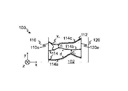
Fig. 1 is a schematic illustration of a superconductor device according to a
first embodiment.
The device comprises a graphite structure 100, more specifically its topmost
layers 102 along
the vertical direction z (pointing into the plane of the figure).
The topmost layers 102 comprise wrinkles 114, which are line defects with
respect to the
(regular) planar arrangement of the carbon atoms in the topmost layers 102.
More specifically,
the carbon atoms of the wrinkles 114 are displaced out of a plane x, y
corresponding to flat
sections of the topmost layers 102 with the (regular) planar arrangement of
the carbon atoms
therein. In other words, the wrinkles 114 protrude along the (negative)
vertical direction (-)z
from the plane x, y defined by the flat sections of the topmost layers 102.
The wrinkles ii4a, 114b, ii4c are sufficiently close to each other to allow
for an electronic
coupling between them, which is beneficial for establishing room-temperature
superconductivity. In other words, a spacing, or distance, respectively,
between the wrinkles
114 is no larger than a critical value for a sufficient electronic coupling.
Our experiments
indicate that this critical value is in the range from 2 to 200 nm, and
presumably in the range
from 2 to wo nm.
21
Date Recue/Date Received 2023-03-07
Various approaches may be applied to characterize the distance between the
wrinkles 114a,
11413, 114c.
One relevant approach is to use the smallest distance di between a pair 114a,
11413; 114b, 114c
of wrinkles. The sections of the wrinkles 114a, 11413, 114c defining the
minimum distance
contribute significantly to the electronic coupling and therefore to the
superconductivity.
Another relevant approach uses the average distance d between each pair 114a,
114b of
neighboring wrinkles. This approach gives a measure of the overall/average
electronic
coupling between the wrinkles 114a, 11413 along their respective lengths
between the electrodes
110, 120. According to the example depicted in Fig. 1, the wrinkles 114a,
11413, 114c each extend
essentially along a direction x parallel to a surface or an interface of the
graphite structure 100
defined by the topmost layer 102. They are spaced apart essentially along the
direction y. To
determine the average, the average position T. of each wrinkle along the
direction y is first
determined, and then the average distance d is measured between the average
positions T..
The plurality 114 of wrinkles 114a, 114b, 114c are located within a (wrinkle)
region 112 of the
topmost layers 102. The outermost wrinkles 114a, 114c of the plurality 114
form boundaries of
the wrinkle region 112.
Electrodes 110, 120 are arranged on the topmost layers 102 and contact the
wrinkles 114
electrically at different positions corresponding to the edges 110e, 120e of
the electrodes.
The electrodes 110, 120 or their respective edges noe, 120e contacting the
wrinkles 114 may be
considered to form boundaries of the wrinkle region 112.
As will be laid out in more detail throughout the disclosure, this structure
implements a high-
temperature superconductor with a critical temperature exceeding room
temperature, even at
ambient pressure, or a room-temperature superconductor, respectively.
Figure 2 gives the detailed view to schematically illustrate a possible
structure of a wrinkle 114.
The figure may be considered a cross section through one of the wrinkles 114a,
11413, 114c of
the wrinkle region 112 of figure 1 parallel to the y, z plane.
Graphite has a layered structure of (carbon) atoms, wherein layers
characterized by atomic
distances of <0.2 nm therein are separated from each other by a layer spacing
206, 216
> 0.3 nm.
According to the embodiment of figure 2, the wrinkle 114 extends through three
topmost
atomic layers 102a, 102b, 102C of the graphite. In alternative embodiments,
the wrinkle 114
may extend through two, four, five, six, or more topmost atomic layers 114.
22
Date Recue/Date Received 2023-03-07
Bulk atomic layers 214 below the topmost atomic layers 114 are essentially
flat and not
modified by the wrinkle 114. According to the example, three bulk atomic
layers 214 are shown,
but many more bulk atomic layers 214 may be present, such as 10, 102, 103,
104, 105, 106, 107 or
more.
The wrinkle 114 bends out of the surface with radii R1, R2 in the nanometer
range, for example
in a range from 1 to 100 nm. Correspondingly, the bending radius r at the
upper end of the
wrinkle 114 lies in a similar range.
Consequently, the height 202 and the width 204 which may be used for an
alternative
characterization (as compared to the radii R1, R2, r) are also in the
nanometer range.
The radii R1, R2, r (or height 202 and width 204, respectively) in the
nanometer range result
in a change of the atomic arrangement at and/or in the wrinkle 114 as compared
to the regular
arrangement of (carbon) atoms in graphite, for example in the flat sections of
the topmost
atomic layers 102 or in the bulk atomic layers 214.
For example, the interlayer spacing 206 in and/or at the wrinkle 114 amounts
to 0.336 to
0.344 nm and is larger than the atomic layer spacing 216 of the bulk atomic
layers 214
(0.335 nm).
Moreover, the stacking sequence of the (topmost) atomic layers 102a, 102b,
102C changes at
and/or in the wrinkle 114. This is illustrated in figure 2 by depicting the
atoms 208 in the
section 210 outside the wrinkle 114 as well as in the section 212 of the
wrinkle 114.
According to the example of figure 2, in the section 210 outside the wrinkle
114, the atoms of
the first topmost atomic layer 102a and of the third topmost atomic layer 102C
are arranged
directly (along the plane x, y) on top of each other. This type of stacking is
referred to as Bernal.
In contrast, in the section 212 of the wrinkle 114 the atoms of the first
topmost atomic layer
102a, of the second topmost atomic layer 102b, and of the third topmost atomic
layer 102C are
each displaced with respect to each other. This type of stacking is different
from the one in the
section 210 outside of the wrinkle as an effect of the bending radius Ri. The
change in the
stacking influences the electronic structure and may give rise to the
superconductivity.
According to the stacking depicted in the section 212 of the example of figure
2, the atoms of a
fourth topmost atomic layer (if present with wrinkles under the third topmost
atomic layer
102c) may be arranged directly (along the plane x, y) under the atoms of the
first topmost
atomic layer 102a. Such an arrangement is referred to as rhombohedral, and
commonly
realized in graphite.
A change of the atomic arrangement at and/or in the wrinkle 114 as compared to
the regular
arrangement of (carbon) atoms in graphite may result in a local modification
of the electronic
23
Date Recue/Date Received 2023-03-07
structure of the graphite, and a local superconductivity. The extended
geometry of the wrinkle
114 and the coupling of the wrinkles in the wrinkle region 112 perpendicular
to the wrinkles 114
as illustrated in Fig. 1 converts and transfers this local superconductivity
into a
superconductivity characterized by a zero-resistance state supporting a
dissipationless current
transport through the wrinkle region 112, or between the electrodes 110, 120,
respectively.
Fig. 3a, Fig. 3h, Fig. 3c, Fig. 3d, and Fig. 3e depict modifications of the
superconductor device
of Fig. 1. Various modifications are described in the context of these
figures. According to
different embodiments, one, all or any combination of the described
modifications may be
implemented.
The embodiment of Fig. 3a is similar to the one of Fig. 1. However, pairs
114a, 114b; 114c, 114d
of wrinkles 114 of the embodiment of Fig. 3a comprise parallel sections 116a,
116h; 116h, 116c.
These parallel sections beneficially contribute to and enhance the electronic
coupling between
the wrinkles 114, and thus to the critical temperature of the superconductor
device.
The distance d2 between the parallel sections 116a, 116h, 116c may serve as a
measure for the
distance between the wrinkles 114.
According to the embodiment, the parallel sections 116a, 116b; 116b, 116c
coincide with sections
of minimum distance between the wrinkles 114a, 114b; 114b, 114c. This
arrangement is not
necessary, but beneficial for enhancing the coupling between the wrinkles
114a, 114b, 114c.
According to the embodiment, the wrinkles 114 have straight segments 116a,
116b, 116c which
(at least in part) coincide with the parallel sections 116a, 116b, 116c. This
arrangement is not
necessary, but beneficial for enhancing the coupling between the wrinkles
114a, 114b, 114c.
According to the embodiment, each pair of wrinkles 114a, 114b; 114b, 114c
comprises respective
parallel sections 116a, 116h; 116b, 116c. This arrangement is not necessary,
but beneficial for
enhancing the coupling between the wrinkles 114a, 114b, 114c. According to
alternative
embodiments, only a portion of the wrinkles 114 comprises parallel sections.
The embodiment of Fig. 3h is similar to the one of Fig. 1. However, the pair
of wrinkles 114a,
114b of Fig. 3h exhibits a crossing (intersection) 126, and the pair of
wrinkles 114b, 114c exhibits
a branching 128.
The crossing (intersection) 126 and the branching 128 are characterized by the
distance
between the wrinkles 114a, 114b becoming zero.
At the crossing (intersection) 126, the number of wrinkles 114 in the
reference planes 126a,
126b is the same. The reference planes 126a, 126b are perpendicular to the
direction x along
which the wrinkles 114 extend and arranged at different positions along the
direction x, one
before and one after the crossing (intersection) 126.
24
Date Recue/Date Received 2023-03-07
At the branching 128 the numbers of wrinkles 114 in the reference planes 128a,
128b differ.
The reference planes 128a, 128b are perpendicular to the direction x along
which the wrinkles
114 extend and arranged at different positions along the direction x, one
before and one after
the branching 128.
Branchings 128 and/or intersections 126 enhance the coupling between the
wrinkles 114
further and support the formation of current paths for a dissipationless,
superconducting
current through the wrinkle region 112.
The embodiment of Fig. 3c is similar to the one of Fig. 1. However, the
wrinkles 114a, 114b, 114c
of Fig. 3c exhibit a first wrinkle direction 118a in the vicinity of the
electrode no, which is
perpendicular to the (edge noe of the) electrode no. Moreover, the wrinkles
114b, 114c exhibit
a second wrinkle direction 118b in the vicinity of the second electrode 120,
which is
perpendicular to the (edge 12oe of the) second electrode 120. In other words,
the electrodes
110, 120 contact the wrinkles 114b, 114c essentially at a 90 angle
(perpendicularly). The
wrinkle 114a gets contacted electrically by the first electrode no at a 90
angle
(perpendicularly).
Contacting the wrinkles 114 with the electrodes 110, 120 at a 90 angle has
proven beneficial
for driving a significant dissipationless (superconducting) current through
the wrinkle region
112 using the electrodes 110, 120. In other words, the perpendicular
contacting improves the
critical current of the superconductor device.
According to the embodiment of Fig. 3c, each wrinkle 114a, 114b, 114c of the
plurality 114 of
wrinkles has the same first wrinkle direction 118a in the vicinity of the
electrode no, or at its
contact to the edge line, respectively. However, a beneficial effect may still
be achieved when
only some (such as a quarter, a third, half) of the wrinkles 114 have the
first wrinkle direction
118a. The same holds true for the second wrinkle direction 118b in the
vicinity of the second
electrode 120. According to the example of Fig. 3c, the wrinkles 114b, 114c
have the second
wrinkle direction 118b.
The embodiment of Fig. 3d is similar to the ones of Fig. 1, Fig. 3c. However,
the electrodes 110,
120 have been formed with a shape ensuring that they 110, 120 are
perpendicular to the first
wrinkle direction 118a and the second wrinkle direction 118b.
The embodiment of Fig. 3e is similar to the ones of Fig. 1, Fig. 3a, Fig. 3c,
and Fig. 3d. The
embodiment combines several of the beneficial characteristics described above
in the context
of those embodiments. The wrinkles 114 of Fig. 3e each have straight, parallel
sections 116a,
116b, 116c, 116d (see Fig. 3a). The wrinkles 114 each have a first (second)
wrinkle direction 118a
(118b) in the vicinity of the first (second) electrode no (120), with a 90
angle between the first
(second) wrinkle direction 118a (118b) and the first (second) electrode no
(120).
Date Recue/Date Received 2023-03-07
Each of the wrinkles 114d has a neighboring wrinkle on its first side (towards
the positive
direction y of Fig. 3e) and an opposite neighboring wrinkle on its opposite
side (towards the
negative direction y of Fig. 3e), each with a spacing, or distance,
respectively, no larger than
the critical value for the sufficient electronic coupling. In the context of
this disclosure,
corresponding wrinkles 114d are referred to as densely packed wrinkles 114d or
as a dense
wrinkle array 114d. They define, in combination with the electrodes 110, 120
if present, a dense
wrinkle region 112d. In contrast to the wrinkle region 112, which may comprise
sections
without wrinkles 114, the dense wrinkle region 112d is completely filled with
a dense wrinkle
array 114d.
The dense wrinkle array of Fig. 3e consists of two wrinkles 114d, but it may
contain more
wrinkles or a single wrinkle, such as the wrinkle 114b of Fig. 1, Fig. 3a,
Fig. 3h, Fib. 3c, Fig. 3d.
Fig. 4a, Fig. 4h depict modifications of the superconductor device of Fig. 1,
Fig. 3a, Fig. 3h, Fig.
3c, Fig. 3c, Fig. 3d, and Fig. 3e. Various modifications are described in the
context of these
figures. According to different embodiments, one, all or any combination of
the described
modifications may be implemented.
The embodiments depicted in Fig. 4a, Fig. 4h comprise multiple electrodes 110,
120, 130, 140,
150, 160, 170. A wrinkle region 112, 122, 132, 142, 152, 162 is located
between each pair of
electrodes 110, 120, 130, 140, 150, 160, 170, or between corresponding edges
150e, 160e, of the
electrodes 150, 160 respectively. (Only some of the edges are indicated by
reference numerals,
but corresponding edges exist for all electrodes 110, 120, 130, 140, 150, 160,
170, typically on
two sides of the electrodes 120, 130, 140, 150, 160.)
Each wrinkle region 112, 122, 132, 142, 152, 162 comprises multiple dense
wrinkle regions 112d,
122d, 132d, 142d, 152d, 162d. The wrinkle regions 112d, 122d, 132d, 142d,
152d, 162d indicated
by the dashed lines are continuous. In other words, they do not comprise any
flat section with
a width exceeding the critical width.
The superconductor device of Fig. 4a, Fig. 4h further comprises conductive
wiring now, 170w
to a current source 300. The wiring now, i7ow encounters the electrodes 110,
170 at contacts
noc, 170c, thus connecting the electrodes 110, 170 to the current source 300.
The current
source 300 provides a current J below the critical current of the
superconductor device, which
the superconductor device transports between the electrodes 110, 170 and
through the wrinkle
regions 112, 122, 132, 142, 152, 162. According to the embodiments shown in
Fig. 4a and Fig.
4h, wiring now, 170w and contacts noc, 170c to the electrodes 110, 170 are
shown, but
alternatively, or in addition, electrodes 120, 130, 140, 150, 160 may be
provided with wiring to
the current source 300 and contacts (not shown).
26
Date Recue/Date Received 2023-03-07
Corresponding embodiments allow for extending the superconductor device to an
enhanced
length along one or two dimensions.
The embodiment depicted in figure 4a further comprises an isolated wrinkle
114', i. e. a wrinkle
114' without any neighboring wrinkle within a spacing, or distance,
respectively, within the
critical value required for the sufficient electronic coupling. In other
words, the wrinkle 114' is
not part of a pair or a dense wrinkle array. The isolated wrinkle 114' does
not contribute to the
superconductivity of the superconductor device, or to the superconducting
current,
respectively. However, the presence of the isolated wrinkle 114' does not
interfere with the
superconductivity, and the isolated wrinkle 114' may be present in the wrinkle
region 112.
In contrast, the dense wrinkle regions 112d, 122d, 132d, 142d, 152d, 162d do
not contain any
isolated wrinkle. As laid out above in the context of Fig. 3e, each dense
wrinkle region 112d,
122d, 132d, 142d, 152d, 162d is entirely filled with a dense wrinkle array
114d, maximizing the
critical current density of the superconducting (dissipationless) current in
these regionsii2d,
122d, 132d, 142d, 152d, 162d.
Fig. 5a and Fig. 5b show measured current voltage characteristics for
different magnetic fields
B and a device layout corresponding to the one of Fig. 4a, Fig. 4h. To
establish the device,
eleven electrodes 110, 120, 130, 140, 150, 160, 170 of silver-doped,
conductive epoxy were
deposited on suitable sections (wrinkle regions 112, 122, 132, 142, 152, 162)
of a surface of
cleaved, highly orientated pyrolytic graphite. The distance between pairs of
neighboring
electrodes 110, 120; 120, 130; 130, 140; 140, 150; 150, 160; 160, 170 (widths
of the wrinkle
regions 112, 122, 132, 142, 152, 162) along the direction x was 0.2 mm.
For each measurement, the current I (A), I (mA) driven through the device with
the current
source 300 is depicted on the lower axis, and the voltage drop V(A) measured
between a pair
of the electrodes 110, 120, 130, 140, 150, 160, 170 is depicted on the left
axis. Fig. 5a depicts the
current voltage characteristics Bo, B2, B5, B9 on a semi-logarithmic scale for
magnetic fields
of o T, 2 T, 5 T, and 9 T. Fig. 5b depicts the current voltage characteristics
on a linear scale for
a magnetic field of 0.2 T. All measurements were performed with the
superconductor device at
a temperature of 300 K.
All measurements depicted in Fig. 5a and Fig. 5b demonstrate that for a
sufficiently small
current driven through the device, the voltage drop V(A) is zero, i. e. below
the resolution
limit (10 nA) of the measurement devices. Consequently, the resistance R of
the
superconductor device, defined by the voltage drop V(A) per current I (A), I
(mA) driven
through the device, R = V/I, is zero within the resolution limit of the
measurement. This is the
case for currents I (A), I (mA) between the electrodes 110, 170 below the
critical current Ic (e.
g. approximately o.o8 mA in Fig. 5b) of the superconductor device. At the
critical current Ic,
the voltage drop V(A) shows a sudden increase towards higher currents 1(A), I
(mA). In other
27
Date Recue/Date Received 2023-03-07
words, the voltage drop 17( A) increases suddenly and significantly, resulting
in a much larger
resistance R = V/I well detectable with the applied measurement devices. For
example, in Fig.
5b, for a current I(mA) of 0.3 mA (> Ic), the voltage drop amounts to
approximately o.6 A,
resulting in a resistance R = o.6 A/0.3 mA.
.. The vanishing (within the resolution limit of the measurement) measured
resistance of the
superconductor device gives direct evidence of dissipationless (within the
resolution limit of
the measurement) current transport through the superconductor device, i.e.
between the
electrodes 110, 120, 130, 140, 150, 160, 170 and/or through the wrinkle
regions 112, 122, 132,
142, 152, 162. In general, the dissipated power P relates to the current 1(A),
I (mA) as P = R 12.
When the resistance R is zero, the dissipated power is zero, and the current I
(A), I (mA) is
dissipationless.
Fig. 6a shows a magnetization curve 6o6 of a superconductor device according
to the
description, and Fig. 6b shows a corresponding reference measurement 6o8 for
the
conventional superconductor Bi2Sr2CaCu208 at a temperature (60 K) below its
critical
temperature (90 K). Therefore, the magnetization M (G), M(mG) of the
respective material
was measured while an external magnetic field H, H (Oe) was applied.
Referring to Fig. 6a, during the measurements, a magnetic field H was applied
perpendicular
to the topmost atomic layer 102, or along the c-axis c of the flat section of
the topmost atomic
layers 102 (coinciding with the c-axis of the bulk atomic layers 214, if
present), respectively.
The superconductor device was kept at a temperature of 300 K for the
measurement. The
magnetization of the superconductor device was measured as the magnetic field
H was ramped
up (as indicated by arrow 602 to the right) and as the magnetic field H was
decreased (as
indicated by arrow 604 to the left). The measured magnetization curve 6o6 is
hysteretic, i. e.
its shape differs significantly depending on whether the magnetic field H is
ramped up 602 or
.. decreased 604.
The magnetization curve 6o6 of Fig. 6a is very similar to the reference
magnetization curve
6o8 measured on the conventional, well-established superconductor
Bi2Sr2CaCu208 (below its
critical temperature) shown in Fig. 6b. The similarity gives direct
experimental evidence that
the graphite structure 100 performs as a superconductor device not only in the
sense that it
supports a dissipationless current, but it also expels an external magnetic
field (shows a
Meissner effect) as the conventional superconductor Bi2Sr2CaCu208 of the
reference
measurement 6o8 does.
The inventors decided to perform the reference measurement on Bi2Sr2CaCu208,
as it has a
layered crystallographic structure, similarly to graphite. For the measurement
6o8 of Fig. 6b,
the magnetic field H was applied perpendicular to the atomic layers of the
Bi2Sr2CaCu208, or
along its c-axis c, respectively.
28
Date Recue/Date Received 2023-03-07
Fig. 6c summarizes the critical currents Ic (mA) determined from multiple
measurements
similar to the ones of Fig. 5a, Fig. 5b for various temperatures T and
magnetic fields B.
For each temperature T (e. g., T = 4.5 K, T = 20 K, T = 100 K, ...) the
critical current Ic (mA)
decreases with increasing magnetic field B (T), as is typically observed for
superconductors.
When observing the critical current Ic (mA) at a given magnetic field B (T)
(i. e., along a vertical
line in Fig. 6c) exceeding a critical field Bcr, the critical current Ic (mA)
increases with
temperature. According to the example of Fig. 6c, the critical field Bcr
amounts to 35 mT. This
behavior is unusual and unique to the best of our knowledge, as the critical
current Ic (mA) of
conventional superconductors decreases with increasing temperature (as
observed for the
superconductor device of Fig. 6c for magnetic fields B (T) below the critical
field Bcr).
The unusual behavior depicted in Fig. 6c makes the superconductor device
according to this
description particularly attractive for applications in environments where a
magnetic field is
present. By operating the superconductor device at a sufficiently high
temperature, the
decrease of the critical current Ic (mA) caused by the magnetic fields B (T)
may be
compensated. For example, the magnetic field may be unintended and otherwise
only be
avoided at the expense of a significant technological effort and corresponding
costs. Other
applications may require a magnetic field for a functionality other than the
superconductivity
(e. g. for an electric motor).
Fig. 7 compares the temperature dependences of the critical current Ic (A) for
a magnetic field
Bo' (o T) below the critical field Bc and for a magnetic field Bi (1 T) above
the critical field Bc.
As discussed above, the former decreases with increasing temperature T (K),
showing a
conventional behavior, whereas the latter increases with temperature T (K)
reflecting the
unique characteristics of the superconductor device according to the
description.
In addition, Fig. 7 depicts the inverse bulk, non-superconducting-state
resistance RN of
graphite using solid lines 7ooa, 700b. In other words, the solid lines 7ooa,
700b depict the
function Ic = c / RN, where c is a constant (0.19 V in the example of Fig.
7). One solid line 7ooa
depicts the function Ic = c / RN using the bulk, non-superconducting-state
resistance RN for a
magnetic field of o T, the other 700b for a magnetic field of 1 T.
On the one hand, the depicted function 7ooa, 700b, Ic = c / RN agrees well
with the measured
critical current Ic, Bo', Bi. On the other hand, the only physical quantity
that the depicted
function 7ooa, 700b, Ic = c / RN relates to is the bulk, non-superconducting-
state resistance
RN of graphite. In combination, these two observations give clear evidence
that the
superconductivity of the superconductor device, characterized by the critical
current Ic, is
mediated by the (normal state) bulk graphite. In other words, the (normal
state) bulk graphite
29
Date Recue/Date Received 2023-03-07
underlying the topmost layers 102 with the wrinkles beneficially contributes
to the
superconductivity.
Fig. 8a illustrates a method for generating 708 a surface 706 of a graphite
basic material 704
with topmost atomic layers 102, and Fig. 8h shows the resulting surface 706.
Referring to Fig. 8a, a suitable graphite basic material 704 is first
provided.
Our experiments indicate that a high degree of parallelism between neighboring
atomic layers
214 of the bulk graphite, and/or of the graphite basic material 704,
respectively, is beneficial
for superconductivity. The parallelism may be characterized by a distribution
of the c-axes of
the bulk atomic layers 214. The c-axis of each atomic layers refers to an axis
perpendicular to
the atomic layer. The c-axis should be aligned within 2 , preferably within
0.5 or within 0.2 .
Moreover, our experiments indicate that a graphite basic material 704 with a
high resistivity
perpendicular to its atomic planes 214 (as compared to the resistivity along
its atomic planes
214) is beneficial for superconductivity. Ideally, the resistivity
perpendicular to the layers 214
is at least 100,000 times larger than the resistivity parallel to the atomic
layers 214.
Highly orientated pyrolytic graphite has proven suitable for the graphite
basic material 704.
Further referring to Fig. 8a, an adhesive tape 702 is attached to the upper
side of the graphite
basic material 704.
Then, the adhesive tape 702 is pulled off the graphite basic material 704
along a direction 700
essentially parallel to the upper side of the graphite basic material 704. The
adhesion between
the adhesive tape 702 and the uppermost layers of the graphite basic material
704 is stronger
than the adhesion between the uppermost layers of the graphite basic material
704 and the
atomic layers of the graphite thereunder. Consequently, pulling off the
graphite basic material
704 along the direction 700 removes the uppermost layers sticking to the
adhesive tape 702
from the graphite basic material 704, and lays open the topmost atomic layers
102 of the
surface 706 generated this way. This process is referred to as cleaving 708.
Bulk atomic layers
214 remain unaltered by the cleaving 708.
Fig. 8h is a schematic view of the surface 706 generated by the cleaving 708
and defined by the
topmost atomic layers 102. Wrinkles 114 perpendicular to the cleaving
direction 700 are found
on the surface 706 after the cleaving 708. At least in part, the wrinkles 114
exhibit parallel
sections 116.
In a next step, wrinkle regions ii2a, 112b on the surface 706 are selected to
exhibit the
properties described above in the context of Fig. 1, Fig. 3a, Fig. 3h, Fig.
3c, Fig. 3d, Fig. 3e. The
sections ii2a, 112b indicated in Fig. 8b give exemplary, possible choices of
such wrinkle regions
112a, 112b.
Date Recue/Date Received 2023-03-07
In a next step, electrodes are deposited onto/over the surface 706 according
to the selected
wrinkle regions ii2a, 112b. In particular, the electrodes are deposited such
that their edges
coincide with the boundaries 710, 712 of the selected wrinkle regions ii2a,
112b perpendicular
to the wrinkles 114 (and parallel to the cleaving direction 700).
Therefore, a mask is provided to shadow the wrinkle regions ii2a, 112b during
the deposition
of the electrodes.
Subsequently, electrically conductive material is deposited onto the surface
706 with the mask
shadowing the wrinkle regions ii2a, 112b to complete the superconductor
device. For example,
the electrically conductive material may be deposited using molecular beam
epitaxy or
chemical vapor deposition, applying techniques we known in the context of
silicon
semiconductor technology, or the conductive material may be deposited from a
liquid phase,
for example in the form of a silver doped, conductive epoxy.
Fig. 9a, Fig. 9b, and Fig. 9c illustrate the generation of wrinkles 114 in the
cleaving 708 process.
Fig. 9a schematically depicts the initial stage of the removal of the adhesive
tape 702 from the
graphite basic material 704 along the direction 700 to generate the surface
706 as described
above in the context of Fig. 8a. Pulling the adhesive tape 702 along the
direction 700 results in
a force along the direction 700 onto the atomic layers of the graphite basic
material 704 in the
vicinity of the adhesive tape 702 and the surface 706.
Fig. 9b schematically depicts a later stage of the removal of the adhesive
tape 702. The force
along the direction 700 has resulted in a partial shift of the topmost atomic
layers 102 along
the direction 700 and led to a wrinkling 114 of the topmost atomic layers 102
near the generated
surface 706. The bulk atomic layers 214 under the topmost atomic layers 102
and sufficiently
far from the surface 706 (separated from the surface 706 by the topmost atomic
layers 102)
remain unaltered by the wrinkling 114.
Fig. 9c schematically depicts the final stage of the removal of the adhesive
tape 702, i. e. the
adhesive tape has fully been removed from the surface 706. The formation of
the wrinkle 114
of the topmost atomic layers 102 perpendicular to the direction 700 is
completed.
Fig. Ina, Fig. lob, and Fig. Inc illustrate alternative methods to generate
wrinkles 114 and the
topmost atomic layers of graphite, preferably with a parallel arrangement of
the wrinkles 114.
Fig. loa shows a top view of the cleaving 708, which is been described above
in detail in the
context of Fig. 8a, Fig. 9a, Fig. 9b, Fig. 9c. As the wrinkles 114 generated
by the cleaving 708
are each essentially perpendicular to the cleaving direction 700, they exhibit
long, parallel
sections 116. These are formed in the cleaving process 708 essentially
parallel to an interface
31
Date Recue/Date Received 2023-03-07
separating the graphite basic material 704 with adhesive tape 702 on top from
the surface 706
of the graphite basic material 704 generated in the cleaving 708 process.
Fig. lob illustrates the formation 8 oo of wrinkles 114 in the topmost layers
102 using a sound
or light source 802 emitting sound or light waves 804. The sound or light
waves 804 interact
with an (initially flat) graphite surface to generate the wrinkles 114.
Details of a corresponding
technique using sound waves are given in A.V. Alaferdov, et al., "Ripplocation
in graphite
nanoplatelets during sonication assisted liquid phase exfoliation," Carbon
129, 826e829
(2018). Details of a corresponding technique using light waves are given in T.
Zou et al., "High-
speed femtosecond laser plasmonic lithography and reduction of graphene oxide
for
anisotropic photoresponse," Light: Science & Applications volume 9, 69 (2020).
Fig. Inc illustrates the formation 810 of wrinkles 114 in the topmost layers
102 using a nano-
or microprobe 812. The nano- or microprobe 812 interacts with an (initially
flat) graphite
surface to generate a force parallel to the surface plane x, y in the topmost
atomic layers 102.
This force ultimately results in the wrinkling 114 of the topmost atomic
layers 102. Details are,
for example, given in B. Jayasena et al., "A novel mechanical cleavage method
for synthesizing
few-layer graphenes," Nanoscale Research Letters 6, 95 (2011) or in X. Lu et
al., "Tailoring
graphite with the goal of achieving single sheets," Nanotechnology 10, 269
(1999).
The description of the embodiments and the drawings merely serve to illustrate
the present
disclosure and the advantageous effects associated therewith, but should not
be understood to
imply any limitation. The scope of the disclosure is determined by the
appended claims.
32
Date Recue/Date Received 2023-03-07
LIST OF REFERENCE SIGNS
100 graphite structure
102, 102a, 102b, 102C at least one topmost atomic layer
110 first electrode
noc contact
noe edge of first electrode
now wiring of first electrode
112, 122, 132, 142, 152, 162 wrinkle region
112d, 122d, 132d, 142d, 152d, 162d dense wrinkle array
114 plurality of wrinkles
114a, 114b, 114c wrinkle
114d densely-packed wrinkles, wrinkles with
respective
neighboring and opposite neighboring wrinkles
114' isolated wrinkle
116a, 116b, 116c parallel section
118a first wrinkle direction perpendicular to the
first electrode
118b second wrinkle direction perpendicular to the
second
electrode
120 second electrode
120e edge of second electrode
126 crossing
126a first reference plane for crossing
126b second reference plane for crossing
128 intersection
128a first reference plane for intersection
128b second reference plane for intersection
130, 140, 150, 160, 170 electrodes
33
Date Recue/Date Received 2023-03-07
150e, 160e edge of fifth, sixth electrode
i7oc contact
170w wiring of electrode
300 current supply
Bo, B2, B5, B9 voltage-current characteristics for different
magnetic
fields
Bo', Bi temperature-dependence of critical current in
the
absence and presence of magnetic field
Bcr critical magnetic field
602 ramping up the magnetic field
604 decreasing the magnetic field
6o6 magnetization curve of superconductor device
6o8 magnetization curve of reference, conventional
superconductor
700a, 700b solid line; function of bulk, non-
superconducting-state
resistance RN
700 cleaving direction
702 adhesive tape
704 graphite basic material
706 surface
708 cleaving
112a, 11213 region of surface with wrinkles
710 edge of region of surface with wrinkles
712 edge of region of surface with wrinkles
34
Date Recue/Date Received 2023-03-07
8o o generating wrinkles with wave (light, acoustic
wave)
source
802 wave (light, acoustic wave) source
804 wave (light, acoustic wave)
8io generating wrinkles with scanning probe
812 scanning probe
Date Recue/Date Received 2023-03-07