Note : Les descriptions sont présentées dans la langue officielle dans laquelle elles ont été soumises.
WO 2023/283720
PCT/CA2022/050993
MULTI-COLOR OLED ARRAY FOR HIGH APERTURE
DISPLAY
CROSS-REFERENCE TO RELATED APPLICATIONS
[0001] This application claims priority to United States patent application
US17/378,300 filed on
16 July 2021, which is hereby incorporated by reference herein in its
entirety.
FIELD OF THE INVENTION
[0002] The present disclosure relates to a patterning design and fabrication
method for an
organic light emitting diode (OLED) device with a high aperture ratio,
suitable for a light field
display.
BACKGROUND OF THE INVENTION
[0003] Light field displays provide multiple views, allowing a user to receive
a separate view in
each eye. While current displays in this category provide an interesting
viewing experience, a
captivating light field display requires a very high pixel density, very low
angular separation
between views, and a large viewing angle. It is desired that a user
experiences smooth transitions
between viewing zones, while maintaining an independent and perceivable view
from the
adjacent views. A fundamental requirement in achieving these viewing
parameters is controlling
the output characteristics of the emission source. Organic light-emitting
diodes (OLEDs) bound
in a microcavity allow control of the spectral bandwidth and output angle of
the resulting light.
[0004] One method for controlling the output characteristics of light is
through the use of a
microcavity. A microcavity is formed between two mirrors or reflective
surfaces, which can be,
for example, a metal anode, a metal cathode, or a layered stack of non-
absorbing materials,
which can be a distributed Bragg reflector (DBR). The mirror serves to reflect
light in a range of
wavelengths while generally preserving the physical characteristics of the
incident light. Two
main design variables affecting the output characteristics of a microcavity
are the reflectance of
the top and bottom surfaces (i.e. opposing mirrors) and the optical path
length, A. The
wavelength of the light output by such an OLED structure is dependent, in
part, upon the optical
path length of the microcavity. The optical path length can be manipulated by
adjusting the
thickness and/or number of the layers that comprise the microcavity.
1
CA 03225281 2024- 1- 8
WO 2023/283720
PCT/CA2022/050993
100051 When manufacturing OLEDs at the size suitable for a light field
display, challenges arise
when depositing organic layers separately to achieve the thickness required
for each color's
desired optical path length. One challenge for manufacturing OLEDs that are
suitable for a light
field display is to achieve a high aperture ratio with pixels smaller than 10
lam using available
manufacturing capabilities. The aperture ratio of a pixel is the ratio of the
light emitting area of
the pixel to the total area of the display. A high aperture ratio can be
achieved by maximizing the
light emitting area of each pixel on the display This decreases gaps in the
display area, thereby
increasing the image quality of the light field display. It is particularly
challenging to achieve a
high aperture ratio when fabricating high resolution displays with small pixel
sizes.
100061 United States Patent Application Publication US2021/0057670 to Wong et
al. describes
an array of light-emitting OLED pixels. The pixels disclosed use multiple
transparent, or
substantially transparent, dielectric layers on each anode. The thicknesses of
the dielectric layers
are designed to optimize emission of the desired color of light for that
pixel. The white OLED
layers are formed in a single deposition step for the OLED array, and the
lateral spacing between
each anode results in a reduced aperture ratio.
100071 United States Patent 10,790,473 to Park et al. describes an OLED device
designed to
achieve a high aperture ratio. The high aperture ratio is achieved by first
connecting the
reflecting electrode and transparent electrode of the anode at the corner of
the subpixel regions.
Each subpixel has a microcavity structure, minimizing the pixel defining layer
between
subpixels. The spacing between the subpixels is not preferable for a light
field display as the
light emitting area for the display is not maximized.
100081 High aperture ratios are preferred for near eye displays, such as
virtual reality (VR)
displays, augmented reality (AR) displays, micro displays, and light field
displays. There
remains a need for a micron sized OLED pixel array design and method of
fabrication that
achieves a high aperture ratio at a high display resolution suitable for a
light field display.
100091 This background information is provided for the purpose of making known
information
believed by the applicant to be of possible relevance to the present
invention. No admission is
necessarily intended, nor should be construed, that any of the preceding
information constitutes
prior art against the present invention.
2
CA 03225281 2024- 1- 8
WO 2023/283720
PCT/CA2022/050993
SUMMARY OF THE INVENTION
[0010] It is an object of the present disclosure to provide an optical
microcavity pixel device
comprising an organic light emitting diode (OLED) and a photolithography
patterning method
that achieves a micron sized pixel that when patterned in an array achieves an
aperture ratio
greater than 70%. It is another object of the present disclosure to provide a
method of OLED
array patterning that is capable of producing a light field display with a
resolution greater than
1,000 ppi (pixels per inch). The optical microcavity pixel array comprises a
distributed Bragg
reflector (DBR) on a substrate and two or more subpixels comprising a semi-
transparent or fully
transparent electrode, and a series of semi-transparent or fully transparent
optical filler layers. It
is another object of the present disclosure to provide an optical microcavity
pixel design structure
wherein semi-transparent or fully transparent electrodes arranged on the DBR
have a lateral
overlap to reduce lateral spacing, which increases the aperture ratio of the
light field display.
Limiting, reducing, or eliminating the lateral spacing between the colored
electrodes can be
achieved using a layered series of semi-transparent or fully transparent
filler layers interposed
between the overlapping electrodes of a first and second color, a second and
third color, a first
and third color, or any combination thereof. The filler layer thickness is
designed to tune the
optical cavity of each pixel, thereby dictating the color generated by the
optical microcavity pixel
device. It is another object of the present disclosure to provide a method to
reduce the
complexity of the fabrication process of a high aperture OLED array.
[0011] In an aspect there is provided an organic light emitting diode device
comprising. a
substrate; a distributed Bragg reflector (DBR) on the substrate; a first color
electrode on the DBR
defining a first color microcavity, the first color electrode connected to the
substrate through a
first via; a first optical filler layer on the DBR adjacent the first color
electrode; a second optical
filler layer on the first optical filler layer and partially overlapping the
first color electrode at an
overlap region, a second color electrode on the second optical filler layer
defining a second color
microcavity, the second color electrode connected to the substrate through a
second via; a white
organic light emitting diode (OLED) stack on top of the first color electrode
and the second color
electrode; and a top electrode on top of the white OLED stack.
[0012] In an embodiment, the second color electrode partially overlaps the
first color electrode.
3
CA 03225281 2024- 1- 8
WO 2023/283720
PCT/CA2022/050993
100131 In another embodiment, the first color microcavity has a first color
optical path length
between the DBR and the top electrode through the first color electrode and
the second color
microcavity has a second color optical path length between the DBR and the top
electrode
through the second color electrode.
100141 In another embodiment, the first color optical path length and the
second first color
optical path length are tuned to provide desired first color and second color
pixels, respectively.
100151 In another embodiment, the first optical filler layer and the second
optical filler layer
comprises a transparent polymer.
100161 In another embodiment, the first optical filler layer and the second
optical filler layer
comprises a transparent inorganic dielectric.
100171 In another embodiment, the device further comprises a pixel definition
layer insulating
the first color electrode from the second color electrode.
100181 In another embodiment, the pixel definition layer comprises one or more
of an inorganic
insulating dielectric and an organic material.
100191 In another embodiment, the substrate is a thin film transistor (TFT)
substrate.
100201 In another embodiment, the device further comprises a second DBR on top
of the top
electrode.
100211 In another embodiment, the top electrode is a cathode and the bottom
electrode is an
anode.
100221 In another embodiment, the top electrode is an anode and the bottom
electrode is a
cathode.
100231 In another embodiment, the device further comprises, on top of the
second color
electrode and under the white OLED stack: a third optical filler layer on the
first optical filler
layer defining a third color microcavity; a fourth optical filler layer on the
third optical filler
layer, the fourth optical filler layer partially overlapping the second color
electrode; and a third
color electrode on the fourth optical filler layer and partially overlapping
the second color
electrode, the third color electrode connected to the substrate through a
third via
4
CA 03225281 2024- 1- 8
WO 2023/283720
PCT/CA2022/050993
[0024] In another aspect there is provided a method for fabricating a multi-
colored microcavity
organic light emitting diode (OLED) array, the method comprising: depositing a
distributed
Bragg reflector (DBR) on a substrate; depositing a first color electrode on
the DBR defining a
first color microcavity, the first color electrode connected to the substrate
through a first via;
depositing a first optical filler layer on the DBR adjacent the first color
electrode; depositing a
second optical filler layer on the first optical filler layer partially
overlapping the first color
electrode at an overlap region; depositing a second color electrode on the
second optical filler
layer defining a second color microcavity, the second color electrode
connected to the substrate
through a second via; depositing a white organic light emitting diode (OLED)
stack on top of the
first color electrode and the second color electrode; and depositing a top
electrode on top of the
white OLED stack.
[0025] In an embodiment of the method, the white OLED stack is deposited over
the entire
OLED array
100261 In another embodiment of the method, the white OLED stack is deposited
using thermal
evaporation, spin casting, or inkjet printing.
[0027] In another embodiment of the method, the top electrode is deposited
using thermal
evaporation or sputtering.
[0028] In another embodiment, the method further comprises depositing a pixel
definition layer
insulating the first color electrode from the second color electrode.
[0029] In another embodiment of the method, the pixel definition layer is
deposited using
sputtering, spin coating, thermal evaporation, chemical vapor deposition,
atomic layer
deposition, or spin casting.
[0030] In another embodiment, the method further comprises depositing a second
DBR on the
top electrode.
[0031] In another embodiment of the method, the first color electrode, the
second color
electrode, and the top electrode are deposited using sputtering, thermal
evaporation, or spin
coating.
CA 03225281 2024- 1- 8
WO 2023/283720
PCT/CA2022/050993
[0032] In another embodiment of the method, the first optical filler layer and
the second optical
filler layer are deposited using sputtering, thermal evaporation, chemical
vapor deposition, or
atomic layer deposition.
100331 In another embodiment of the method, the DBR is deposited using
sputtering, thermal
evaporation, chemical vapor deposition, or atomic layer deposition.
[0034] In another embodiment, the method further comprises, prior to
depositing the white
OLED stack: depositing a third optical filler layer selected for a third color
on top of the first
optical filler layer, the third optical filler layer overlapping the first
color electrode; depositing a
fourth optical filler layer selected for a third color on top of the third
optical filler layer, the
fourth optical filler layer overlapping the second color electrode; and
depositing a series of third
color electrodes on the fourth optical filler layer.
BRIEF DESCRIPTION OF THE DRAWINGS
100351 These and other features of the invention will become more apparent in
the following
detailed description in which reference is made to the appended drawings.
[0036] FIG. IA illustrates an embodiment of a cross section view of a two
color optical
microcavity organic light emitting diode (OLED) array as per the present
disclosure.
100371 FIG. 1B illustrates an enlarged illustration of a one color optical
microcavity OLED
device as described in FIG. 1A.
100381 FIG. 1C illustrates an enlarged illustration of a two color optical
microcavity OLED
device as described in FIG. 1A.
[0039] FIG. 2 illustrates an alternative embodiment of a two color optical
microcavity OLED
array as per the present disclosure including a pixel definition layer (PDL)
100401 FIG. 3A illustrates an alternative embodiment of a two color optical
microcavity OLED
array as per the present disclosure including an additional DBR deposited on
the cathode.
[0041] FIG. 3B illustrates an enlarged illustration of a two color optical
microcavity OLED
device as described in FIG. 3A.
6
CA 03225281 2024- 1- 8
WO 2023/283720
PCT/CA2022/050993
100421 FIG. 4 illustrates an embodiment of a cross section of a three color
optical microcavity
OLED array as per the present disclosure.
100431 FIG. 5 illustrates an alternative embodiment of a three color optical
microcavity OLED
array as per the present disclosure including a PDL.
100441 FIG. 6 illustrates an alternative embodiment of a three color optical
microcavity OLED
array as per the present disclosure including an additional DBR deposited on
the cathode.
100451 FIG. 7 illustrates an embodiment of a light path from the TFT substrate
to emission of the
two color optical microcavity OLED array as per the present disclosure.
100461 FIG. 8 illustrates an embodiment of a light path from the TFT substrate
to emission of the
three color optical microcavity OLED array as per the present disclosure.
100471 FIG. 9 illustrates the top view of an embodiment of light emission from
the three color
optical microcavity OLED array as per the present disclosure.
100481 FIG. 10A illustrates step 1 of the proposed two color OLED array
patterning process for
depositing a DBR.
100491 FIG. 10B illustrates step 2 of the proposed two color OLED array
patterning process for
forming vias for the first color electrode through the DBR.
100501 FIG. 10C illustrates step 3 of the proposed two color OLED array
patterning process for
depositing a first color electrode.
100511 FIG. 10D illustrates step 4 of the proposed two color OLED array
patterning process for
depositing a photoresist.
100521 FIG. 10E illustrates step 5 of the proposed two color OLED array
patterning process for a
photolithography step, which partially exposes the embodiment to UV light
thereby partially
removing the photoresist through etching.
100531 FIG. 1OF illustrates step 6 of the proposed two color OLED array
patterning process for
depositing a first optical filler layer.
7
CA 03225281 2024- 1- 8
WO 2023/283720
PCT/CA2022/050993
[0054] FIG. 10G illustrates step 7 of the proposed two color OLED array
patterning process for a
photolithography step, which lifts off the remaining photoresist thereby
removing the first optical
filler layer that was deposited on the photoresist.
[0055] FIG. 10H illustrates a top view of step 7 of the proposed two color
OLED array
patterning process.
[0056] FIG. 101 illustrates step 8 of the proposed two color OLED array
patterning process for
depositing a second optical filler layer.
[0057] FIG. 10J illustrates step 9 of the proposed two color OLED array
patterning process for
forming a via for the second color electrode through the DBR, the first
optical filler layer, and
the second optical filler layer.
[0058] FIG. 10K illustrates step 10 of the proposed two color OLED array
patterning process for
depositing a second color electrode.
[0059] FIG. 1 OL illustrates a top view of step 10 of the proposed two color
OLED array
patterning process.
[0060] FIG. 10M illustrates step 11 of the proposed two color OLED array
patterning process for
depositing a white OLED stack.
[0061] FIG. ION illustrates step 12 of the proposed two color OLED array
patterning process for
depositing a cathode as the top reflective surface, forming the optical
microcavity of the OLED
array.
[0062] FIG. 11A illustrates step 1 of the proposed three color OLED array
patterning process for
depositing a DBR.
100631 FIG. 11B illustrates step 2 of the proposed three color OLED array
patterning process for
forming vi as for the first color electrode through the DBR.
[0064] FIG. 11C illustrates step 3 of the proposed three color OLED array
patterning process for
depositing the first color electrode.
100651 FIG. 11D illustrates step 4 of the proposed three color OLED array
patterning process for
depositing a photoresist.
8
CA 03225281 2024- 1- 8
WO 2023/283720
PCT/CA2022/050993
[0066] FIG. 11E illustrates step 5 of the proposed three color OLED array
patterning process for
a photolithography step, which partially exposes the embodiment to UV light
thereby partially
removing the photoresist through etching.
[0067] FIG. 11F illustrates step 6 of the proposed three color OLED array
patterning process for
depositing a first optical filler layer.
[0068] FIG. 11G illustrates step 7 of the proposed three color OLED array
patterning process for
a photolithography step, which lifts off the remaining photoresist thereby
removing the first
optical filler layer that was deposited on the photoresist.
[0069] FIG. 11H illustrates a top view of step 7 of the proposed three color
OLED array
patterning process.
[0070] FIG. 111 illustrates step 8 of the proposed three color OLED array
patterning process for
depositing a second optical filler layer.
[0071] FIG. 11J illustrates step 9 of the proposed three color OLED array
patterning process for
forming a via for the second color electrode through the DBR, the first
optical filler layer, and
the second optical filler layer.
100721 FIG. 11K illustrates step 10 of the proposed three color OLED array
patterning process
for depositing a second color electrode.
[0073] FIG. 11L illustrates a top view of step 10 of the proposed three color
OLED array
patterning process.
[0074] FIG. 11M illustrates step 11 of the proposed three color OLED array
patterning process
for depositing the photoresist.
100751 FIG. 11N illustrates step 12 of the proposed three color OLED array
patterning process
for a photolithography step, which partially exposes the embodiment to UV
light thereby
partially removing the photoresist through etching.
[0076] FIG. 110 illustrates step 13 of the proposed three color OLED array
patterning process
for depositing a third optical filler layer.
9
CA 03225281 2024- 1- 8
WO 2023/283720
PCT/CA2022/050993
100771 FIG. 11P illustrates step 14 of the proposed three color OLED array
patterning process
for a photolithography step, which lifts off the remaining photoresist thereby
removing the third
optical filler layer that was deposited on the photoresist.
[0078] FIG. 11Q illustrates step 15 of the proposed three color OLED array
patterning process
for depositing a fourth optical filler layer.
[0079] FIG. 11R illustrates step 16 of the proposed three color OLED array
patterning process
for forming a via for the third color electrode through the DBR, the first
optical filler layer, the
third optical filler layer, and the fourth optical filler layer.
100801 FIG. 11S illustrates step 17 of the proposed three color OLED array
patterning process
for depositing a third color electrode.
100811 FIG. 11T illustrates a top view of step 17 of the proposed three color
OLED array
patterning process.
100821 FIG. 11U illustrates step 18 of the proposed three color OLED array
patterning process
for depositing a white OLED stack.
100831 FIG. 11V illustrates step 19 of the proposed three color OLED array
patterning process
for depositing a cathode as the top reflective surface to form the optical
microcavity of the
OLED device.
DETAILED DESCRIPTION OF THE INVENTION
Definitions
100841 Unless defined otherwise, all technical and scientific terms used
herein have the same
meaning as commonly understood by one of ordinary skill in the art to which
this invention
pertains.
100851 The use of the word -a" or -an" when used herein in conjunction with
the term
-comprising" may mean -one," but it is also consistent with the meaning of -
one or more," -at
least one" and "one or more than one."
100861 As used herein, the terms "comprising," "having," "including" and
"containing," and
grammatical variations thereof, are inclusive or open-ended and do not exclude
additional,
CA 03225281 2024- 1- 8
WO 2023/283720
PCT/CA2022/050993
unrecited elements and/or method steps. The term "consisting essentially of"
when used herein in
connection with a composition, device, article, system, use, or method,
denotes that additional
elements and/or method steps may be present, but that these additions do not
materially affect the
manner in which the recited composition, device, article, system, method, or
use functions. A
composition, device, article, system, use, or method described herein as
comprising certain
elements and/or steps may also, in certain embodiments comprise essentially of
those elements
and/or steps, and in other embodiments comprise of those elements and/or
steps, whether or not
these embodiments are specifically referred to.
100871 As used herein, the term "about" refers to an approximately +/-10%
variation from a
given value. It is to be understood that such a variation is always included
in any given value
provided herein, whether or not it is specifically referred to.
100881 The recitation of ranges herein is intended to convey both the ranges
and individual
values falling within the ranges, to the same place value as the numerals used
to denote the
range, unless otherwise indicated herein.
100891 The use of any examples or exemplary language, e.g. "such as",
"exemplary
embodiment", "illustrative embodiment" and "for example" is intended to
illustrate or denote
aspects, embodiments, variations, elements or features relating to the
invention and not intended
to limit the scope of the invention.
100901 As used herein, the terms "connect" and "connected" refer to any direct
or indirect
physical association between elements or features of the present disclosure.
These terms may be
understood to denote elements or features that are partly or completely
contained within one
another, attached to, coupled to, disposed on, joined together, in
communication with,
operatively associated with, etc., even if there are other elements or
features intervening between
the elements or features described as being connected
100911 As used herein, the term "OLED" refers to an Organic Light Emitting
Diode, which is an
opto-electronic device which emits light under the application of an external
voltage. OLEDs
have an emissive electroluminescent layer or organic material or species that
emits light in
response to an electric current. OLEDs can be divided into two main classes:
those made with
small organic molecules and those made with organic polymers. Without being
bound by theory,
11
CA 03225281 2024- 1- 8
WO 2023/283720
PCT/CA2022/050993
when a current is applied, the anode injects holes and the cathode injects
electrons into the
organic layers. The injected holes and electrons each migrate toward the
oppositely charged
electrode. When an electron and hole localize on the same molecule, an
exciton, which is a
localized electron-hole pair having an excited energy state, is formed. Light
is emitted when the
exciton relaxes via a photo emissive mechanism. Types of OLED include but are
not limited to
Active-matrix OLEDs (AMOLED) and Passive-matrix OLEDs (PMOLED). AMOLEDs have
full layers of cathode, organic molecules, and anode The anode layers have a
thin film transistor
(TFT) plane in parallel to it so as to form a matrix. This helps in switching
each pixel to its on or
off state as desired, thus forming an image. Hence, the pixels can be switched
off whenever they
are not required or there is a black image on the display, decreasing the
energy required to
illuminate the display. This is the least power consuming type of OLED and has
quicker refresh
rates which makes them suitable for video. PMOLEDs have a similar composition
to AMOLEDs
but the cathode lines are arranged at right angles to the anode lines. The
electrical control is
achieved through the anode and cathode lines to activate the pixel at the
intersection point,
generating light. The display background of a PMOLED is always black while the
color
displayed when the pixel is turned on is a predetermined color. PMOLED pixels
are fixed to a
single color and are not suitable for dynamic imagery or displays. OLEDs may
be top or bottom
emitting. Top-emitting OLEDs have a substrate that is either opaque or
reflective. An OLED is
bottom emitting if the emitted light passes through the transparent or semi-
transparent bottom
electrode and substrate. Top-emitting OLEDs are generally better suited for
active-matrix
applications as they can be more easily integrated with a non-transparent
transistor backplane.
100921 As used herein, the term "DBR" refers to a distributed Bragg reflector.
A distributed
Bragg reflector is an optical mirror which is composed of different dielectric
layers with different
refractive indices in an alternative order.
100931 As used herein, the term "optical path length", denoted by A, refers to
the distance
between two points (P1, P2), accounting for the refractive index (n) of the
material that light
travels through. In an example OLED device, the media that the light travels
through may
comprise one or more semitransparent or transparent intermediate electrodes
and other layers, as
well as layers comprising a white OLED stack. An optical path length is
defined as the function:
12
CA 03225281 2024- 1- 8
WO 2023/283720
PCT/CA2022/050993
P2
A= n1 d1.
P1
100941 As used herein, the term "light field" refers to a function describing
the amount of light
flowing in every direction through points in space. A light field can
represent radiance as a
function of position and direction of light in free space, preferably free of
occlusions. A light
field can be synthetically generated, for example, through various rendering
processes or may be
captured from a light field camera or from an array of light field cameras.
100951 As used herein, the term "light field display" is a device which
reconstructs a light field.
In one example the light field can be reconstructed from a finite number of
light field radiance
samples input to the light field display device. The radiance samples
generally represent the color
components red, green and blue (RGB). For reconstruction in a light field
display, a light field
can also be understood as a mapping from a four-dimensional space to a single
RGB color,
where the four dimensions include the vertical and horizontal dimensions of
the display and two
dimensions describing the directional components of the light field. In one
example, a light field
can be defined as the function:
LF : (x,y, u, v) ¨> (r, g,b)
For a fixed xf, yf, LF(xf,yf,u,v) represents a two-dimensional (2D) image
referred to as an
"elemental image", where the elemental image is a directional image of the
light field from the
fixed xf, yf position. When a plurality of elemental images are connected side
by side, the
resulting image is referred to as an "integral image". The integral image can
be understood as the
entire light field required for the light field display.
100961 As used herein, the term "aperture ratio", in describing an optical
display, refers to the
ratio of the light emitting area compared to the total pixel area defined as
the function:
light emitting area
Aperture ratio = ______________________________________________
total pixel area
[0097] As used herein, the term "pixel" refers to a light source and light
emission mechanism
used to create a display.
13
CA 03225281 2024- 1- 8
WO 2023/283720
PCT/CA2022/050993
100981 As used herein, the term "subpixel" refers to a structure comprised of
a light emitting
device housed within an optical microcavity.
100991 As used herein, the term "electrode" refers to a conductor through
which electricity enters
or leaves an object, substance, or region.
101001 As used herein, the term "cathode" refers to the negatively charged
electrode by which
electrons enter an electrical device
101011 As used herein, the term "anode- refers to the positively charged
electrode by which the
electrons leave an electrical device.
101021 As used herein, the term "patterning" refers to a technique to transfer
pattern upon a
target material.
101031 As used herein, the term "wavelength" is a measure of distance between
two identical
peaks (high points) or troughs (low points) in a wave, which is a repeating
pattern of traveling
energy such as light or sound.
101041 Herein is described a microcavity organic light emitting diode (OLED)
design and
method for tuning a micron sized multi color optical microcavity OLED array. A
light field
display requires a pixel density of at least 25000 pixels per inch (ppi),
requiring each pixel to be
less than 20 lam. Most preferably, light field displays with a high display
resolution have pixel
densities greater than 5,000 ppi. Achieving a high aperture ratio at these
resolutions can be
accomplished through maximizing the light emitting area for each subpixel and
minimizing
subpixel spacing. This disclosure provides an optical microcavity pixel device
comprising an
organic light emitting diode (OLED) and a photolithography patterning method
that achieves a
micron sized pixel that when patterned in an array achieves an aperture ratio
greater than 70%,
suitable for a light field display with a resolution greater than 1,000 ppi.
This can be achieved by
patterning transparent or semi-transparent optical filler layers and
intermediate electrodes to
laterally overlap other intermediate electrodes in the OLED array to reduce
lateral spacing and
increase the aperture ratio of the resulting OLED array. This lateral overlap
design enables the
designer to optimize the optical properties of each OLED device and the
aperture ratio of the
OLED array as a whole. While the industry definition of a high aperture ratio
for a display with
micron sized pixels is 70%, this design allows the display to achieve near or
about a 100%
14
CA 03225281 2024- 1- 8
WO 2023/283720
PCT/CA2022/050993
aperture ratio, creating a high-quality display suitable for a light field
display and other
applications. Also disclosed are methods for designing and fabricating an
array of OLED devices
that emit light including but not limited to yellow, red, green, or blue
light.
101051 Various features of the invention will become apparent from the
following detailed
description taken together with the illustrations in the Figures. The design
parameters, design
method, construction, and use of the optical microcavity OLED design process
and structures
disclosed herein are described with reference to various examples representing
embodiments
which are not intended to limit the scope of the invention as described and
claimed herein. The
skilled technician in the field to which the invention pertains will
appreciate that there may be
other variations, examples and embodiments of the invention not disclosed
herein that may be
practiced according to the teachings of the present disclosure without
departing from the scope of
the invention.
101061 Each OLED in the device comprises an electrode configured to connect
with a substrate,
an optical microcavity including a distributed Bragg reflector (DBR), and a
cathode. The optical
microcavity is operatively associated with, or connected to, one or more
reflective surfaces to
substantially collimate, manipulate, or tune the light. At least one of the
reflective surfaces is a
light propagating reflective surface connected to the optical microcavity to
propagate the light
out of the optical microcavity. The present disclosure provides individually
addressable red,
green, and blue (RGB) subpixels. The subpixel size as presently described is
in a nanoscale to
several microns range. The DBR, as described herein, is comprised of an
alternating stack of
dielectric materials of specific thicknesses, ensuring the optical path length
is a quarter of the
designed wavelength and suitable for use with an OLED of any color The highest
reflectivity of
a DBR is attained when the layer thicknesses are chosen such that the optical
path length of each
layer is one quarter of the resonance wavelength. With each layer having an
optical path length
f ABragg/4, all reflections will add in phase, and the transmissiyity will
decrease exponentially
as a function of mirror thickness. At longer or shorter wavelengths than the
stopband, the
reflections begin to add out of phase, therefore the total reflection
decreases. This gives a broad-
band high-reflectivity region centered on the Bragg wavelength, called the
stop band, with
oscillating side-lobes on either side. The DBR is generally composed of pairs
of two different
dielectric layers with different refractive indices but may also be composed
of multiple dielectric
CA 03225281 2024- 1- 8
WO 2023/283720
PCT/CA2022/050993
materials or other transparent materials with a contrast in n, as long as the
optical path length of
each layer is ABragg/4. The multilayer mirror comprises alternating layers of
substantially non-
absorbing materials of appropriately chosen thickness. Typically, each layer
is of thickness ¨,
4n
where A is advantageously chosen to correspond approximately to the center
wavelength of the
EML emission spectrum, e.g., 500-550 nm. Such mirrors are well known. The
reflectivity of the
mirror depends in a known way on the number of layer pairs, layer thickness
and the refractive
index of the materials used. Exemplary material pairs in the visible
wavelength region are Si3N4,
SiO2, and TiO2.
101071 FIG. lA illustrates an embodiment of a cross section of a two color
optical microcavity
OLED array as described herein with two OLED devices of the first color and
one OLED device
of the second color. The OLED array shown comprises a DBR 12 deposited on a
substrate 10. In
this embodiment the substrate 10 is a TFT substrate, which is a device that
forms the base
structure of an embodiment of an OLED, providing the electrical control to
switch each pixel or
subpixel to its on or off state as desired. A TFT contains several layers
including a metallic gate
electrode, a gate insulator, a semiconductor layer, and source/drain
electrodes deposited on a
substrate. The TFT substrate preferably also has a planarization layer on
which the materials of
an OLED are deposited. The DBR 12 comprises a series of alternating high
refractive index
dielectric layers 76 and low refractive index dielectric layers 78. The number
of high refractive
index dielectric layers 76 and low refractive index dielectric layers 78 can
be configured to be
any integer. In the embodiment shown the DBR 12 can act as the first
reflective surface for the
optical microcavity of each OLED device in the OLED array.
101081 Before each electrode in a series of electrodes for an array of first
color OLED devices,
herein referred to as the first color electrodes 14A, 14B are deposited on the
DBR 12, a via for
each of the first color OLEDs, herein referred to as the first color via 16A,
16B, is dry etched
through the DBR 12. This provides an electrical connection from the substrate
10 to the first
color electrodes 14A, 14B. The first color vias 16A,16B may be etched using an
etching
technique, for example, reactive ion etching, anodic plasma etching,
magnetically enhanced
reactive ion etching, triode reactive ion etching, or transmission-coupled
plasma etching. In this
embodiment, a preferred dry etching method is used, such as reactive ion
etching. After the first
color vias 16A, 16B are etched through the DBR 12, the first color electrodes
14A, 14B are
16
CA 03225281 2024- 1- 8
WO 2023/283720
PCT/CA2022/050993
deposited on the DBR 12 using a shadow mask. A first optical filler layer 18
is patterned using
photolithography for each second color OLED device in the OLED array directly
on the DBR
12, between the first color electrodes 14A, 14B. The patterning can, for
example, use a series of
post treatments to chemically engrave a transferred pattern into or allow the
deposition of new
material in the transferred material. A second optical filler layer 20 is then
patterned through a
shadow mask, or using photolithography, for each second color OLED device in
the OLED array
on the first optical filler layer 18, covering the first optical filler layer
18 The second optical
filler layer 20 may overlap the first color electrodes 14A, 14B, to form
overlap regions 80A,
80B. The overlap regions 80A, 80B provide tolerances that mitigate alignment
errors in
fabrication, thus increasing the aperture ratio of the display by reducing the
lateral spacing
between the OLED devices on the substrate 10. The optical filler layers are
designed to be
transparent to visible light and electrically insulating. The optical filler
layers function as
electrically insulating layers to prevent crosstalk between the first color
electrodes 14A, 14B and
the second color electrode 22 in the overlap regions 80A, 80B.
101091 Before a second color electrode 22 is deposited on the second optical
filler layer 20, a
second color via 24 for each of the second color electrodes 22 is dry etched
using reactive ion
etching through the second optical filler layer 20, the first optical filler
layer 18, and the DBR 12.
The second color via 24 provides an electrical connection from the substrate
10 to the second
color electrode 22. The second color electrode 22 is then patterned on the
second optical filler
layer 20 with a shadow mask, preferably wherein the width of the second color
electrode 22 is
the same as the width of the second optical filler layer 20. For a two-color
OLED array the layers
of the white OLED stack 26 are then deposited over the entire OLED array. In a
three color
OLED array, a third optical filler layer, a fourth optical filler layer, third
color via, and third
color electrode would be deposited for the third color, followed by the white
OLED stack 26.
The uniformly deposited OLED stack emits white light, and for each color
optical microcavity,
the optical path length is tuned to achieve the specific color. A cathode 28
is then deposited on
the white OLED stack 26 using, for example, a thermal evaporation deposition
method. In this
embodiment, the cathode 28 is a reflective material, deposited with a
thickness resulting in a
transmission greater than 0%, and is used to form the optical microcavity of
each OLED device.
17
CA 03225281 2024- 1- 8
WO 2023/283720
PCT/CA2022/050993
101101 In this embodiment, the substrate 10 comprises a non-conducting
component that forms
the base for the OLED device and a conducting component that electrically
powers each
electrode. One example can be a thin film transistor (TFT) substrate comprised
of one or more
semiconducting materials, a gate insulator, and a substrate. The
semiconducting materials can
include, for example, hydrogenated amorphous silicon, polycrystalline silicon,
amorphous oxide
semiconductors, cadmium selenide, zinc oxide, organic materials such as
pentacene, poly (3-
hexylthiophene), poly (3-alkylthiophene), and poly (3-octylthiophene), or
transparent electrodes
such as indium zinc oxide (IZO) or indium tin oxide (ITO). Indium tin oxide
(ITO) is typically
encountered as an oxygen-saturated composition with a formulation of 74% In,
18% 02, and 8%
Sn by weight. ITO is also commonly used as an anode material in an OLED
structure due to its
suitable conductivity, nearly transparent and colorless optical properties,
and that it can be
deposited by well-established methods. ITO can also be used to construct the
anode layer in
OLED devices according to the present disclosure. The gate insulator can be a
metal passivated
material with a transparent insulator such as SiO2 and Si3N4or an organic
material such as poly-
methyl methacrylate. The substrate can also be a non-conducting material, such
as glass. The
DBR 12 comprises alternating high refractive index dielectric layers 76 and
low refractive index
dielectric layers 78, that may be comprised of TiO2 and SiO2. The first color
electrodes 14A, 14B
and second color electrode 22 can be a semitransparent or transparent
conducting material, such
as ITO, a conducting polymer such as doped polyaniline, or a thin layer
(between 5 and 35 nm,
preferably less than 10 nm) of metal or alloy, or a carbon based material such
as graphene.
Transparent conducting materials, such as ITO, are preferred due to their high
transmittance
values (80-85%) and low reflectivity and absorbance.
[OM] The first optical filler layer 18 and second optical filler layer 20 can
be, for example, a
transparent polymer, such as, for example polyimi de, or an inorganic
transparent dielectric with
various refractive index values, such as, for example, A1203, SiO2, or Si3N4.
The first optical
filler layer 18 and second optical filler layer 20 can be comprised of the
same material or
different materials. The optical filler layers 18, 20 can be deposited
through, for example,
sputtering, thermal evaporation, chemical vapor deposition, or atomic layer
deposition. One
preferred method of deposition is sputtering, which allows the designer to
precisely adjust the
thickness of the layers during deposition. The thickness of the optical filler
layers and the
materials that comprise them are designed to tune the optical path length for
each specific colour.
18
CA 03225281 2024- 1- 8
WO 2023/283720
PCT/CA2022/050993
The preferred material for an optical filler layer has a refractive index
similar to the bottom
electrodes. For example, ITO can be used for the second color electrode 22 and
A1203 can be
used for both the first optical filler layer 18 and the second optical filler
layer 20. The white
OLED stack 26 comprises thin-film layers of organic material, which commonly
include one or
more of an Organic Hole-Injection Layer (HIL), an Organic Hole-Transporting
Layer (HTL), an
Emissive Layer (EML), an Organic Electron-Transporting Layer (ETL), and an
Organic
Electron-Injection Layer The series of layers in the white OLED stack are
designed to emit
white light. The individual colors of each OLED device are achieved through
tuning the optical
path length for each optical microcavity. Each layer of the white OLED stack
26 can be
deposited through thermal evaporation, spin casting, or inkjet printing. For
this embodiment, one
preferred method for deposition of the white OLED stack 26 is thermal
evaporation. The cathode
28 can be a reflective metal with a reflectance greater than 90%, such as
aluminum, cadmium, or
silver. This embodiment illustrates a conventional OLED configuration, wherein
the bottom first
color electrodes 14A, 14B and second color electrode 22 below the white OLED
stack 26 are
anodes, and the top electrode above the white OLED stack 26 is a cathode 28.
The microcavity
OLEDs described herein have a substantially reflective top and bottom surface
with substantially
transparent intermediate layers that collectively create a resonance inside
the optical microcavity
to create the optical path length required for the desired color. In the
present configuration,
wherein the DBR 12 is the bottom reflective surface and the cathode 28 is the
top reflective
surface, the cathode 28 is marginally less reflective than the DBR 12,
allowing light generated in
the optical microcavity to be emitted through the top of the OLED array. In
another arrangement,
the OLED array may be configured as an array of inverted OLED devices, wherein
the bottom
electrodes, deposited under the white OLED stack 26, are fully transparent
cathodes and the top
electrodes above the white OLED stack are reflective anodes. The presently
described OLED
array may also be configured to be an array of bottom emitting OLED devices,
wherein the
bottom electrode, the DBR 12, and the substrate 10 are marginally less
reflective than the top
electrode, emitting light through the substrate 10. The present OLED array can
also be
configured to be comprised of any combination of inverted or non-inverted and
top or bottom
emitting OLEDs.
[0112] In an optical microcavity, the optical path length for each color is
equal to the peak
wavelength of the color divided by two and multiplied by a positive integer.
19
CA 03225281 2024- 1- 8
WO 2023/283720
PCT/CA2022/050993
Therefore:
Acx
Acx = m-
2
where:
Ac, is the optical path length of a color
m is an integer
Ac, is the peak wavelength of a color
101131 Each element that comprises the optical microcavity has an optical path
length that is
determined by the refractive index of the material and its thickness. The
total optical path length
for each color can be determined by the optical path length of each element
that comprises the
optical microcavity: the DBR 12, the electrodes 14, 22, the optical filler
layers 18, 20, the white
OLED stack 26, and the cathode 28. Since the DBR 12 and cathode 28 are
reflective surfaces
that form the bounds of the optical microcavity, the penetration depth into
the DBR 12 and the
cathode 28 are considered in addition to the refractive index and the
thickness. In this
embodiment, the DBR 12 and cathode 28 are uniform and the white OLED stack 26
is designed
to emit white light for the entire OLED array. The optical path lengths for
each color include the
penetration depth of the DBR 12 and the penetration depth of the cathode 28.
These penetration
depths are incorporated in design considerations and are constant across the
OLED array. The
DBR 12 and the cathode 28 are present, however not used to tune the optical
path length to emit
a specific color.
Therefore:
Ac1 = Ae1 AOLED (ACATHODE ADBR)
Ac2 = Afi Af2 11e2 AoLED (ACATHODE ADBR)
101141 The optical path length for each first color OLED device in the OLED
array, Aci, herein
referred to as the optical path length of the first color 30A, 30B, is
determined by the optical path
length of the first electrode for each first color OLED device in the OLED
array, herein referred
to as the optical path length of the first electrode (Aei) 34A, 34B and the
optical path length of
the white OLED stack (AoLED) 32. The optical path length for each second color
OLED device in
CA 03225281 2024- 1- 8
WO 2023/283720
PCT/CA2022/050993
the OLED array, Ac2, herein referred to as the optical path length of the
second color (Ac2) 36, is
determined by the sum of the optical path length of the first optical filler
layer (An) 38, the
optical path length of the second optical filler layer (At) 40, the optical
path length of the second
color electrode (Ae2) 42, and the optical path length of the white OLED stack
(AnrE,D) 32. Since
the optical path length of each element in the optical microcavity is
determined by the thickness
of the element and its refractive index, adjusting the thicknesses of specific
elements within the
optical microcavity allows the designer to optimize the optical path length of
the desired color
As the white OLED stack 26 is deposited across the OLED array, the optical
path length of the
white OLED stack (AoLED) 32 can be designed to tune the optical path length
for the first color
(Aci) 30A, 30B, which can be accomplished through optimizing the thickness of
the white
OLED stack 26. In particular, the optical path length for the first color (AO
should be about or
equal to the peak wavelength of the first color divided by two, times an
integer. As the optical
path length of the white OLED stack 32 is uniform across the OLED array the
optical path length
of the second optical filler layer (Ac) 40 can also be designed taking into
consideration the
thickness of the second optical filler layer 20 to create the optical path
length required for the
second color (Ac2) 36. It is advantageous to optimize the optical path length
for the first color
30A, 30B with the optical path length of the white OLED stack 32 and the
optical path length of
the second color 36 with the optical path length of the second optical filler
layer 40, as the white
OLED stack 26 can be uniform. The uniform white OLED stack 26 can then be
deposited over
the entire OLED array, thereby simplifying fabrication.
101151 FIG. 1B illustrates an enlarged illustration of a single color optical
microcavity OLED
device as described in FIG. 1A. The OLED device comprises a DBR 12 deposited
on a substrate
10, which can be a TFT substrate. The DBR 12 comprises a series of alternating
high refractive
index dielectric layers 76 and low refractive index dielectric layers 78. It
is noted that the number
of pairs of high and low refractive index dielectric layers 76, 78 shown in
FIG. 1B is three,
comprising six layers, however the DBR can be comprised of any integer number
of layers. This
composition allows the DBR 12 to act as the first reflective surface for the
optical microcavity of
each OLED device in the OLED array. A first color electrode 14 is deposited on
the DBR 12
through the use of a shadow mask. The layers that comprise the white OLED
stack 26 are then
individually deposited over the entire OLED array. Each layer of the white
OLED stack 26 can
be deposited through, for example, thermal evaporation, spin casting, and
inkjet printing, and
21
CA 03225281 2024- 1- 8
WO 2023/283720
PCT/CA2022/050993
preferably by thermal evaporation. For this embodiment, the white OLED stack
26 can comprise
one or more of each of the following layers: an Organic Hole-Injection Layer
(HIL) 84, an
Organic Hole-Transporting Layer (HTL) 86, an Emissive Layer (EML) 88, an
Organic Electron-
Transporting Layer (ETL) 90, and an Organic Electron-Injection Layer (EIL) 92.
In some
configurations, a white OLED stack 26 can comprise of a single EML 88, wherein
the emission
molecules of specific colors are combined in the EML 88 to generate white
light. In alternate
configurations, a white OLED stack 26 can comprise of multiple EMLs 88, which
can be
referred to as a tandem or stacked white OLED. In a tandem white OLED, white
light is
generated from all emitting EMLs 88 in the white OLED stack 26. In tandem OLED
configurations, an additional charge generation layer can be deposited to
function as an
additional injection layer and as an artificial metal electrode. The
combination of organic layers
in the white OLED stack 26 are designed to emit white light, while each
optical microcavity
tunes the optical path length of various elements to achieve a specific color.
A cathode 28 is then
deposited on the white OLED stack 26 using, for example, thermal evaporation.
In this
embodiment, the cathode 28 is a reflective material and is used to form an
optical microcavity
for each OLED device.
101161 FIG. IC illustrates an enlarged illustration of a two color optical
microcavity OLED
device as described in FIG. 1A. The OLED device comprises a DBR 12 deposited
on a substrate
10. In this embodiment the substrate 10 is a TFT substrate. The DBR 12
comprises a series of
alternating high refractive index dielectric layers 76 and low refractive
index dielectric layers 78.
The number of high and low refractive index dielectric layers 76, 78 can be
configured to be any
integer. This composition allows the DBR 12 to act as the first reflective
surface for the optical
microcavity of each OLED device in the OLED array. A first color electrode 14
is deposited on
the DBR 12 through the use of a shadow mask A first optical filler layer 18 is
patterned using
photolithography for each second color OLED device in the OLED array directly
on the DBR
12, adjacent to the first color electrode 14. A second optical filler layer 20
is then patterned
through a shadow mask or using photolithography for each second color OLED
device in the
OLED array on the first optical filler layer 18, covering the entire first
optical filler layer 18 and
may overlap the first color electrode 14, to form the overlap region 80. The
overlap region 80
mitigates alignment errors in fabrication, thus increasing the aperture ratio
of the display through
reducing the lateral spacing between the OLED devices on the substrate 10. The
second color
22
CA 03225281 2024- 1- 8
WO 2023/283720
PCT/CA2022/050993
electrode 22 is patterned on the second optical filler layer 20 with a shadow
mask, preferably
wherein the width of the second color electrode 22 is the same width as the
second optical filler
layer 20. Although only first and second microcavities are shown here it is
understood that an
OLED array comprises a plurality of first color microcavities with first
electrodes and a plurality
of second color microcavities with second electrodes. It is further understood
that OLED arrays
also generally comprise a plurality of three different color microcavities to
provide red, green,
and blue color emission
101171 The layers that comprise the white OLED stack 26 are then individually
deposited over
the entire OLED array. Each layer of the white OLED stack 26 can be deposited
through thermal
evaporation, spin casting, or inkjet printing. For this embodiment, the
preferred method is
thermal evaporation. For this embodiment, the organic layers that comprise the
white OLED
stack 26 are deposited on the first and second color electrodes 14, 22 in the
following order: an
Organic Hole-Injection Layer (Hit) 84, an Organic Hole-Transporting Layer
(HTL) 86, an
Emissive Layer (EML) 88, an Organic Electron-Transporting Layer (ETL) 90, and
an Organic
Electron-Injection Layer (EIL) 92. The white OLED stack 26 can further
comprise one or more
of each of the organic layers. The organic layers of the white OLED stack 26
are together
designed to emit white light, while each optical microcavity tunes the optical
path length of
various elements to achieve a specific color. A cathode 28 is then deposited
on the white OLED
stack 26 using, for example, thermal evaporation. In this embodiment, the
cathode 28 is a
reflective material and is used to form an optical microcavity for each OLED
device.
101181 FIG. 2 illustrates an alternative embodiment of a two color optical
microcavity OLED
array as per the present disclosure including a pixel definition layer (PDL)
44. This cross section
illustrates two OLED devices of the first color and one OLED device of the
second color. The
OLED array comprises a DBR 12 deposited on a substrate 10. In this embodiment
the substrate
is a TFT substrate, which is a device that forms the base structure of the
embodiment. The
DBR 12 comprises a series of alternating high refractive index dielectric
layers 76 and low
refractive index dielectric layers 78. Before the first color electrodes 14A,
14B are deposited on
the DBR 12, a first color via 16A, 16B is dry etched through the DBR 12 to
provide an electrical
connection from the substrate 10 to the first color electrodes 14A, 14B. In
this embodiment, the
preferred dry etching method is reactive ion etching. The first color
electrodes 14A, 14B are then
23
CA 03225281 2024- 1- 8
WO 2023/283720
PCT/CA2022/050993
patterned on the DBR 12 using a shadow mask. The first optical filler layer 18
is patterned using
photolithography on the DBR 12 between the first color electrodes 14A, 14B.
The second optical
filler layer 20 is deposited on, and fully covers the first optical filler
layer 18 and may overlap
the first color electrodes 14A, 14B, to form overlap regions 80A, 80B. The
second optical filler
layer can be patterned using a shadow mask or photolithography. The overlap
regions 80A, 80B
provide tolerances that mitigate alignment errors in fabrication, thus
increasing the aperture ratio
of the display through reducing the lateral spacing between OLED devices on
the substrate 10
101191 Before the second color electrode 22 is deposited, a second color via
24 is dry etched
using reactive ion etching through the optical filler layers 20, 18 and the
DBR 12 to provide an
electrical connection to the substrate 10. The second color electrode 22 is
patterned with a
shadow mask on the second optical filler layer 20, wherein the width of the
second color
electrode 22 equals the width of the second optical filler layer 20. In this
embodiment, an
optional PDL 44 is patterned with a shadow mask such that it covers the region
of the second
color electrode 22 and second optical filler layer 20 that overhangs the
adjacent first color
electrodes 14A, 14B. The PDL 44 prevents electrical shorting between the first
color electrodes
14A, 14B, and second color electrode 22, reducing crosstalk across the OLED
array. Crosstalk
generally refers to light leaking from one pixel to another when light is
emitted that can interfere
with the image quality causing loss of contrast, loss of depth resolution,
viewer discomfort, and
duplication of displayed images. The PDL 44 can be deposited by, for example,
sputtering, spin
coating, thermal evaporation, chemical vapor deposition, atomic layer
deposition, or spin casting.
The optional PDL 44 can be comprised of an inorganic material such as an
insulating dielectric,
for example A1203, Si3N4, or SiO2, or an organic material such as a
photosensitive polyimide. In
a three color OLED device a PDL layer can also connect the third color
electrode to the second
color electrode. The layers that comprise the white OLED stack 26 are
deposited over the entire
OLED array. A cathode 28 is then deposited by thermal evaporation on the white
OLED stack
26. In this embodiment, the cathode 28 is a reflective material and therefore
is used to form an
optical microcavity for each OLED device.
101201 The optical path length of the first color (Aci)30A, 30B, is determined
by the optical
path length of the first electrode (Aei) 34A, 34B and the optical path length
of the white OLED
stack (AoLED) 32. The optical path length of the second color (Ac2) 36, is
determined by the sum
24
CA 03225281 2024- 1- 8
WO 2023/283720
PCT/CA2022/050993
of the optical path length of the first optical filler layer (An) 38, the
optical path length of the
second optical filler layer (Al2) 40, the optical path length of the second
color electrode (Ae2) 42,
and the optical path length of the white OLED stack (Aorrn) 32. Since the
optical path length of
each element in the optical microcavity is determined by the thickness of the
element and its
refractive index, adjusting the thicknesses of specific elements within the
optical microcavity
allows the designer to tune the optical path length of the desired color. As
the white OLED stack
26 is deposited across the OLED array; the optical path length of the white
OLED stack (A0LED)
32 may be designed to tune the optical path length for the first color (AO
30A, 30B, which may
be accomplished through optimizing the thickness of the white OLED stack 26.
As the optical
path length of the white OLED stack 32 is uniform across the OLED array the
optical path length
of the second optical filler layer (Ac) 40 may be designed through the
thickness of the second
optical filler layer 20 to create the optical path length required for the
second color (Ac2) 36.
101211 Optimizing the optical path length for the first color 30A, 30B with
the optical path
length of the white OLED stack 32 and the optical path length of the second
color 36 with the
optical path length of the second optical filler layer 40 is advantageous as
the white OLED stack
26 can be uniform. The uniform white OLED stack 26 can then be deposited over
the entire
OLED array, thereby simplifying fabrication.
101221 FIG. 3A illustrates an alternative embodiment of a two color optical
microcavity OLED
array having a second DBR 12B deposited on top of the cathode 28. This cross
section illustrates
two OLED devices of the first color and one OLED device of the second color.
The OLED array
comprises a first DBR 12A deposited on a substrate 10. In this embodiment the
substrate 10 is a
TFT substrate, which is a device that forms the base structure of the
embodiment_ The first DBR
12A has a series of alternating high refractive index dielectric layers 76 and
low refractive index
dielectric layers 78. Before the first color electrodes 14A, 14B are deposited
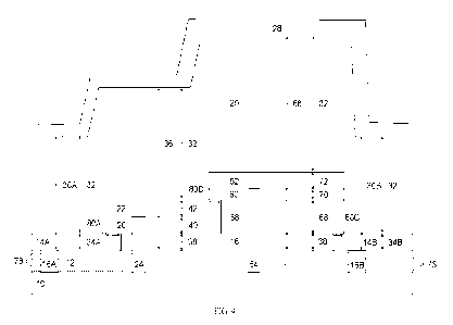
on the first DBR
12A, first color vias 16A, 16B are dry etched through the first DBR 12A to
provide an electrical
connection from the substrate 10 to the first color electrodes 14A, 14B. In a
preferable
embodiment, the vias are created using reactive ion etching. The first color
electrodes 14A, 14B
are then patterned using a shadow mask onto the first DBR 12A. A first optical
filler layer 18 is
then patterned using photolithography on the first DBR 12A between the first
color electrodes
14A, 14B. The second optical filler layer 20 is then deposited such that it
fully covers the first
CA 03225281 2024- 1- 8
WO 2023/283720
PCT/CA2022/050993
optical filler layer 18 and preferably overlap the first color electrodes 14A,
14B, to form overlap
regions 80A, 80B. The second optical filler layer 20 can be patterned using a
shadow mask or
using photolithography. The overlap regions 80A, 80B provide tolerances that
mitigate
alignment errors in fabrication, thus increasing the aperture ratio of the
display through reducing
the lateral spacing between OLED devices on the substrate 10.
101231 Before the second color electrode 22 is deposited, a second color via
24 is dry etched
using reactive ion etching through the optical filler layers 20, 18 and the
first DBR 12A to
provide an electrical connection to the substrate 10. The second color
electrode 22 is patterned
on the second optical filler layer 20 using a shadow mask, wherein the width
of the second color
electrode 22 is approximately equal to the width of the second optical filler
layer 20. The layers
that comprise the white OLED stack 26 are then deposited over the entire OLED
array. A
cathode 28 is then deposited by thermal evaporation on the white OLED stack
26. In this
embodiment, an additional DBR 12B is deposited on top of the cathode 28. The
second DBR
12B has a series of alternating high refractive index dielectric layers 76 and
low refractive index
dielectric layers 78 The cathode 28 is comprised of a semi-transparent or
transparent material
and the DBR 12B is used to form an optical microcavity for each OLED device.
101241 Each element that comprises the optical microcavity has an optical path
length that is
determined by the refractive index of the material and its thickness. The
total optical path length
for each color can be determined by the optical path length of each element
that comprises the
optical microcavity: the first DBR 12A, the first electrodes 14A, 14B, second
electrode 22, the
optical filler layers 18, 20, the white OLED stack 26, the cathode 28, and the
second DBR 12B.
Since the first DBR 12A and second DBR 12B are reflective surfaces that form
the bounds of the
optical microcavity, the penetration depth into the DBRs 12A, 12B are
considered in addition to
the refractive index and the thickness. In this embodiment, the DBRs 12A, 12B
and cathode 28
are uniform and the white OLED stack 26 is designed to emit white light for
the entire OLED
array. The optical path lengths for each color include the penetration depth
of the first DBR 12A,
the penetration depth of the second DBR 12B, and the optical path length of
the cathode 28.
These penetration depths and corresponding optical path lengths are
incorporated in design
considerations but are constant across the OLED array. The first DBR 12A, the
second DBR
12B, and the cathode 28 are not used to tune the optical path length to emit a
specific color.
26
CA 03225281 2024- 1- 8
WO 2023/283720
PCT/CA2022/050993
Therefore:
¨ "el AOLED (ACATHODE ADBR A ADBR B)
AC2 = Afi Af2 Ae2 AoLED (ACATHODE ADBR A ADBR B)
101251 The optical path length of the first color (AO 30A, 30B, is determined
by the optical
path length of the first electrode (Aei) 34A, 34B and the optical path length
of the white OLED
stack (AoLED) 32. The optical path length of the second color (Ac2) 36, is
determined by the sum
of the optical path length of the first optical filler layer (An) 38, the
optical path length of the
second optical filler layer (An) 40, the optical path length of the second
color electrode (Ae2) 42,
and the optical path length of the white OLED stack (Amyx)) 32 Since the
optical path length of
each element in the optical microcavity is determined by the thickness of the
element and its
refractive index, adjusting the thicknesses of specific elements within the
optical microcavity
allows the designer to tune the optical path length of the desired color. As
the white OLED stack
26 is deposited across the OLED array the optical path length of the white
OLED stack (AoLED)
32 can be designed to tune the optical path length for the first color (Aci)
30A, 30B, which can
be accomplished through optimizing the thickness of the white OLED stack 26.
As the optical
path length of the white OLED stack 32 is uniform across the OLED array the
optical path length
of the second optical filler layer (An) 40 can also be designed through the
thickness of the
second optical filler layer 20 to create the optical path length required for
the second color (Ac2)
36. Optimizing the optical path length for the first color 30A, 30B with the
optical path length of
the white OLED stack 32 and the optical path length of the second color 36
with the optical path
length of the second optical filler layer 40 is advantageous as the white OLED
stack 26 can be
uniform across the OLED optical microcavity array. The uniform white OLED
stack 26 can also
be deposited over the entire OLED array, thereby simplifying fabrication.
101261 FIG. 3B illustrates an enlarged illustration of a two color optical
microcavity OLED
device as described in FIG. 3A. The OLED device comprises a first DBR 12A
deposited on a
substrate 10 which is preferably a TFT substrate. The first DBR 12A is
comprised of alternating
high refractive index dielectric layers 76 and low refractive index dielectric
layers 78. The
number of layers of high and low refractive index dielectric layers 76, 78 can
any integer of
layers, with three pairs comprising six layers shown in this configuration. In
this embodiment the
first DBR 12A acts as the first reflective surface for the optical microcavity
of each OLED
27
CA 03225281 2024- 1- 8
WO 2023/283720
PCT/CA2022/050993
device in the OLED array. A first color electrode 14 is deposited on the first
DBR 12A through
the use of a shadow mask. A first optical filler layer 18 is patterned using
photolithography for
each second color OLED device in the OLED array directly on the first DBR 12A,
adjacent to
the first color electrode 14. A second optical filler layer 20 is then
patterned through a shadow
mask or photolithography for each second color OLED device in the OLED array
on the first
optical filler layer 18, covering the entire first optical filler layer 18 and
may overlap the first
color electrode 14, to form the overlap region 80 The overlap region 80
mitigates alignment
errors in fabrication, thus increasing the aperture ratio of the display
through reducing the lateral
spacing between the OLED devices on the substrate 10. The second color
electrode 22 is
patterned on the second optical filler layer 20 with a shadow mask, preferably
wherein the width
of the second color electrode 22 is the same the width of the second optical
filler layer 20.
[0127] The layers that comprise the white OLED stack 26 are then individually
deposited over
the entire OLED array. Each layer of the white OLED stack 26 can be deposited
through, for
example, thermal evaporation, spin casting, or inkjet printing. For this
embodiment, a preferred
method is thermal evaporation. The organic layers that comprise the white OLED
stack 26 are
then deposited on the first and second color electrodes 14, 22 in the
following order: an Organic
Hole-Injection Layer (HIL) 84, an Organic Hole-Transporting Layer (HTL) 86, an
Emissive
Layer (EML) 88, an Organic Electron-Transporting Layer (ETL) 90, and an
Organic Electron-
Injection Layer (EIL) 92. The white OLED stack 26 can comprise of one or more
of each of the
organic layers. The organic layers are designed to emit white light, while
each optical
microcavity tunes the optical path length of various elements to achieve a
specific color. A
cathode 28 is then deposited on the white OLED stack 26 using, for example,
thermal
evaporation. In this embodiment, the cathode 28 is comprised of a semi-
transparent or
transparent material and a second DBR 12B is deposited on the cathode 28. The
second DBR
12B comprises a series of alternating high refractive index dielectric layers
76 and low refractive
index dielectric layers 78. The number of layers of high and low refractive
index dielectric layers
76, 78 in the second DBR 12B can also be configured to be any integer. This
configuration
allows the second DBR 12B to act as the top reflective surface for the optical
microcavity of
each OLED device in the OLED array.
28
CA 03225281 2024- 1- 8
WO 2023/283720
PCT/CA2022/050993
101281 FIG. 4 illustrates an embodiment of a cross section of a three color
optical microcavity
OLED array per the present disclosure. The OLED array comprises a DBR 12
deposited on a
substrate 10. This cross section illustrates two OLED devices of the first
color and a single
OLED device for each of the second color and third color. In this embodiment
the substrate 10 is
a TFT substrate, which is a device that forms the base structure for the OLED
array. The DBR 12
comprises a series of alternating high refractive index dielectric layers 76
and low refractive
index dielectric layers 78, where the number of layers of high refractive
index dielectric layers
76 and low refractive index dielectric layers 78 can be any integer. In this
composition, the DBR
12 is the first reflective surface for the optical microcavity of each OLED
device in the OLED
array.
101291 Before the first color electrodes 14A, 14B for an array of first color
OLED devices are
deposited on the DBR 12, first color vias 16A, 16B are dry etched through the
DBR 12 to
provide an electrical connection from the substrate 10 to the first color
electrodes 14A, 14B. The
vias may be etched by, for example, reactive ion etching, anodic plasma
etching, magnetically
enhanced reactive ion etching, triode reactive ion etching, and transmission-
coupled plasma
etching. One preferred dry etching method for constructing the vias is
reactive ion etching. After
the first color vias 16A, 16B are etched through the DBR 12, the first color
electrodes 14A, 14B
are patterned on the DBR 12 using a shadow mask. A first optical filler layer
18 is then patterned
using photolithography directly on the DBR 12 between the first color
electrodes 14A, 14B for
each second color OLED device in the OLED array. A second optical filler layer
20 is then
deposited on, and partially covers the first optical filler layer 18 and may
overlap the first color
electrode 14A, to form an overlap region 80A. The second optical filler layer
20 can be patterned
using a shadow mask or photolithography. The overlap region 80A provide
tolerances that
mitigate alignment errors in fabrication, thus increasing the aperture ratio
of the display through
reducing the lateral spacing between OLED devices on the substrate 10.
101301 Before a second color electrode 22 is deposited on the second optical
filler layer 20, a
second color via 24 is dry etched using reactive ion etching through the
second optical filler layer
20, the first optical filler layer 18, and the DBR 12. The second color via 24
provides an
electrical connection from the substrate 10 to the second color electrode 22.
The second color
electrode 22 is then patterned using a shadow mask on the second optical
filler layer 20,
29
CA 03225281 2024- 1- 8
WO 2023/283720
PCT/CA2022/050993
preferably wherein the width of the second color electrode 22 is the same the
width of the second
optical filler layer 20. A third optical filler layer 58 is then patterned
using photolithography for
each third color OLED device in the OLED array on the first optical filler
layer 18 adjacent to
the second optical filler layer 20 and may overlap the first color electrode
14B to form an overlap
region 80C. A fourth optical filler layer 60 is deposited for each third color
OLED device in the
OLED array on the third optical filler layer 58 and may overlap the second
color electrode 22, to
form an overlap region 80111 The fourth optical filler layer 60 can be
patterned using a shadow
mask or photolithography. The overlap regions 80C, 80D can mitigate alignment
errors in
fabrication and increase the aperture ratio of the display through reducing
the lateral spacing
between OLED devices on the substrate 10.
101311 Before a third color electrode 62 is deposited on the fourth optical
filler layer 60, a third
color via 64 is dry etched, preferably using reactive ion etching, through the
fourth optical filler
layer 60, the third optical filler layer 58, the first optical filler layer
18, and the DBR 12. The
third color via 64 provides an electrical connection from the substrate 10 to
the third color
electrode 62. The third color electrode 62 is then patterned using a shadow
mask on the fourth
optical filler layer 60, preferably wherein the width of the third color
electrode 62 is the same
width of the fourth optical filler layer 60. The layers that comprise a white
OLED stack 26 are
then deposited over the entire OLED array. A cathode 28 is then deposited on
the white OLED
stack 26 using, for example, thermal evaporation. In this embodiment, the
cathode 28 is a
reflective material and therefore is used to form an optical microcavity for
each OLED device.
101321 In this embodiment, the substrate 10 can be a thin film transistor
(TFT) substrate
comprised of semiconducting materials, a gate insulator, and a substrate The
semiconducting
materials may include, for example, hydrogenated amorphous silicon,
polycrystalline silicon,
amorphous oxide semiconductors, cadmium selenide, zinc oxide; organic
materials, such as
pentacene, poly (3-hexylthiophene), poly (3-alkylthiophene), and poly (3-
octylthiophene); or
transparent electrodes, such as ITO. The gate insulator can be a metal
passivated with a
transparent insulator such as SiO2 and Si3N4or an organic material such as
poly-
methylmethacrylate. The substrate can also be a non-conducting material, such
as glass. The
DBR 12 comprises alternating high refractive index dielectric layers 76 and
low refractive index
dielectric material layers 78. The electrodes 14A, 14B, 22, 62 can be a
semitransparent or
CA 03225281 2024- 1- 8
WO 2023/283720
PCT/CA2022/050993
transparent conducting material, such as ITO, a conducting polymer such as
doped polyaniline,
or a thin layer (between 5 and 35 nm, preferably less than 10 nm) of metal or
alloy, and a carbon
based material such as graphene. The transparent conducting materials such as
ITO are preferred
for this disclosure due to its high transmittance (80-85%) and low
reflectivity and absorbance.
The optical filler layers 18, 20, 58, 60 can comprise transparent polymers,
such as polyimide, or
inorganic transparent dielectrics with various refractive index values such as
A1203, SiO2, or
Si3N4 The optical filler layers 18, 20, 58, 60 can be deposited through
sputtering, thermal
evaporation, chemical vapor deposition, atomic layer deposition. The preferred
material for an
optical filler layer has a refractive index similar to the bottom electrodes;
for example ITO is the
preferred material for the second color electrode 22 and the third color
electrode 62, then A1203
is the preferred material for the optical filler layers. The preferred method
of deposition is
sputtering, which allows the designer to precisely adjust the thickness of the
layers during
deposition. The white OLED stack 26 comprises thin-film layers of organic
material, which
commonly include one or more of an Organic Hole-Injection Layer (Hit), an
Organic Hole-
Transporting Layer (HTL), an Emissive Layer (EML), an Organic Electron-
Transporting Layer
(ETL), and an Organic Electron-Injection Layer. The series of OLED layers are
designed to emit
white light. Each layer of the white OLED stack 26 can be deposited through
thermal
evaporation, spin casting, and inkjet printing. For this embodiment, the
preferred method is
thermal evaporation. The individual colors of each OLED device are achieved
through
modulating the optical path length for each optical microcavity. The cathode
28 can be a
reflective metal with a reflectance greater than 90% such as aluminum,
cadmium, or silver. This
embodiment illustrates a conventional OLED configuration wherein the bottom
electrodes 14A,
14B, 22, 62, below the white OLED stack 26 are anodes and the electrode above
the white
OLED stack 26 is a cathode 28. The present disclosure may also be configured
as an array of
inverted OLED devices, wherein the bottom electrode, deposited before the
white OLED stack
26, is a cathode 28, and the top electrode above the white OLED stack 26 is an
anode. The
present disclosure may also be configured to be an array of bottom emitting
OLED devices,
wherein the bottom electrode, the DBR 12, and the substrate 10 are semi-
transparent or
transparent, emitting light through the substrate 10. The disclosed embodiment
can be configured
to be any combination of inverted or non-inverted and top or bottom emitting.
31
CA 03225281 2024- 1- 8
WO 2023/283720
PCT/CA2022/050993
101331 Each element that comprises the optical microcavity has an optical path
length that is
determined by the refractive index of the material and its thickness. The
total optical path length
for each color can be determined by the optical path length of each element
that comprises the
optical microcavity: the DBR 12, the electrodes 14, 22, 62, the optical filler
layers 18, 20, 58, 60,
the white OLED stack 26, and the cathode 28. Since the DBR 12 and cathode 28
are reflective
surfaces that form the bounds of the optical microcavity, the penetration
depth into the DBR 12
and the cathode 28 are considered in addition to the refractive index and the
thickness In this
embodiment, the DBR 12 and cathode 28 are uniform and the white OLED stack 26
is designed
to emit white light for the entire OLED array. The optical path lengths for
each color include the
penetration depth of the DBR 12 and the penetration depth of the cathode 28.
These penetration
depths are incorporated in design considerations but are constant across the
OLED array. The
DBR 12 and the cathode 28 shown are not used to tune the optical path length
to emit a specific
color.
Therefore:
A ci ¨ "el AOLED (ACATHODE ADBR)
Ac2 = Afi AR 11,2 AoLED (ACATHODE ADBR)
Ac3 = Af1 Ar3 Ae3 AoLED (ACATHODE ADBR)
101341 The optical path length for each first color OLED device in the OLED
array, Aci, herein
referred to as the optical path length of the first color 30A, 30B, is
determined by the optical path
length of the first electrode for each first color OLED device in the OLED
array, herein referred
to as the optical path length of the first electrode (Aei) 34A, 34B and the
optical path length of
the white OLED stack (AoLED) 32. The optical path length for each second color
OLED device in
the OLED array, Ac2, herein referred to as the optical path length of the
second color (Ac2) 36, is
determined by the sum of the optical path length of the first optical filler
layer (An) 38, the
optical path length of the second optical filler layer (At) 40, the optical
path length of the second
color electrode (Ae2) 42, and the optical path length of the white OLED stack
(A0LED) 32. The
optical path length for each third color OLED device in the OLED array, AC3,
herein referred to
as the optical path length of the third color (Ac3) 66, is determined by the
sum of the optical path
length of the first optical filler layer (AO 38, the optical path length of
the third optical filler
32
CA 03225281 2024- 1- 8
WO 2023/283720
PCT/CA2022/050993
layer (Ar3) 68, the optical path length of the fourth optical filler layer
(AN) 70, the optical path
length of the third color electrode (Ae3) 72, and the optical path length of
the white OLED stack
(AoLED) 32.
101351 Since the optical path length of each element in the optical
microcavity is determined by
the thickness of the element and its refractive index, adjusting the
thicknesses of specific
elements within the optical microcavity allows the designer to optimize the
optical path length of
the desired color. As the white OLED stack 26 is deposited across the OLED
array, the optical
path length of the white OLED stack (AoLED) 32 can be designed to tune the
optical path length
for the first color (Act) 30A, 30B, which can be accomplished through
optimizing the thickness
of the white OLED stack 26. In particular, the optical path length for the
first color (Act) 30A,
30B should be about or equal to the peak wavelength of the first color divided
by two, times an
integer. As the optical path length of the white OLED stack 32 is uniform
across the OLED array
the optical path length of the second optical filler layer (Af2) 40 can also
be designed taking into
consideration the thickness of the second optical filler layer 20 to tune the
optical path length
required for the second color (Ac2) 36. Similarly, the optical path length of
the fourth optical
filler layer (Atli) 70 can be designed taking into consideration the thickness
of the fourth optical
filler layer 62 to tune the optical path length required for the third color
(Ac3) 66. Optimizing the
optical path length for the first color 30A, 30B with the optical path length
of the white OLED
stack 32, as well as the optical path length of the second color 36 and the
optical path length of
the third color 66, with the optical path length of the optical filler layers
40, 70 is advantageous
as the white OLED stack 26 can be uniform. The uniform white OLED stack 26 can
then be
deposited over the entire OLED array, thereby simplifying fabrication.
101361 FIG. 5 illustrates an alternative embodiment of a three color optical
microcavity OLED
array as per the present disclosure including a pixel definition layer (PDL)
44. This cross section
illustrates two OLED devices of the first color and a single OLED device for
each of the second
color and third color. The OLED array comprises a DBR 12 deposited on a
substrate 10. In this
embodiment the substrate 10 is a TFT substrate, which is a device that forms
the base structure
of the embodiment. The DBR 12 comprises a series of alternating high
refractive index dielectric
layers 76 and low refractive index dielectric layers 78. Before the first
color electrodes 14A, 14B
are deposited, a first color via 16A, 16B is dry etched through the DBR 12 for
each first color
33
CA 03225281 2024- 1- 8
WO 2023/283720
PCT/CA2022/050993
electrode 14A, 14B to provide an electrical connection to the substrate 10. In
this embodiment,
the preferred dry etching method is reactive ion etching. The first color
electrodes 14A, 14B are
patterned on the DBR 12 using a shadow mask. The first optical filler layer 18
is patterned using
photolithography on the DBR 12 between the first color electrodes 14A, 14B.
The second optical
filler layer 20 is deposited on, and partially covers the first optical filler
layer 18 and may overlap
the first color electrode 14A, to form an overlap region 80A. The second
optical filler layer 20
can be patterned using a shadow mask or photolithography The overlap region
80A provide
tolerances that mitigate alignment errors in fabrication, thus increasing the
aperture ratio of the
display through reducing the lateral spacing between OLED devices on the
substrate 10. A
second color via 24 is then dry etched using reactive ion etching through the
optical filler layer
18, 20 and the DBR 12 to provide an electrical connection for the second color
electrode 22 to
the substrate 10. The second color electrode 22 is patterned using a shadow
mask on the second
optical filler layer 20, wherein the width of the second color electrode 22
equals the width of the
second optical filler layer 20. The third optical filler layer 58 is patterned
using photolithography
on the first optical filler layer 18 adjacent to the second optical filler
layer 20 and may overlap
the first color electrode 14B, to form an overlap region 80C. The fourth
optical filler layer 60 is
deposited on the third optical filler layer 58 and may overlap the second
color electrode 22, to
form an overlap region 80D. The fourth optical filler layer 60 can be
patterned with a shadow
mask or photolithography. The overlap regions 80C, 80D may mitigate alignment
errors in
fabrication, thus increasing the aperture ratio of the display through
reducing the lateral spacing
between OLED devices on the substrate 10. A third color via 64 is then dry
etched using reactive
ion etching through the optical filler layer 58, 60 and the DBR 12 to provide
an electrical
connection to the substrate 10 The third color electrode 62 is patterned using
a shadow mask on
the fourth optical filler layer 60, wherein the width of the third color
electrode 62 equals the
width of the fourth optical filler layer 60. In this embodiment, an optional
PDL 44 is patterned
using a shadow mask such that it covers the region of the second and third
color electrodes 22,
62 and optical filler layers 20, 60, 58 that overhangs the respective adjacent
first color electrodes
14A, 14B and second color electrode 22. The PDL 44 is then deposited between
the first color
electrode 14A and second color electrode 22, second color electrode 22 and
third color electrode
62, and third color electrode 62 and first color electrode 14B. The PDL 44 can
reduce crosstalk
across the OLED array and prevent electrical shorting. The layers that
comprise the white OLED
34
CA 03225281 2024- 1- 8
WO 2023/283720
PCT/CA2022/050993
stack 26 are then deposited over the entire OLED array. A cathode 28 is then
deposited on the
white OLED stack 26 using, for example, thermal evaporation. In this
embodiment, the cathode
28 is a reflective material and forms part of the optical microcavity for each
OLED device.
101371 Each element that comprises the optical microcavity has an optical path
length that is
determined by the refractive index of the material and its thickness. The
total optical path length
for each color can be determined by the optical path length of each element
that comprises the
optical microcavity: the DBR 12, the electrodes 14, 22, 62, the optical filler
layers 18, 20, 58, 60,
the white OLED stack 26, and the cathode 28. Since the DBR 12 and cathode 28
are reflective
surfaces that form the bounds of the optical microcavity, the penetration
depth into the DBR 12
and the cathode 28 are considered in addition to the refractive index and the
thickness. In this
embodiment, the DBR 12 and cathode 28 are uniform and the white OLED stack 26
is designed
to emit white light for the entire OLED array. The optical path lengths for
each color include the
penetration depth of the DBR 12 and the penetration depth of the cathode 28.
These penetration
depths are incorporated in design considerations but are constant across the
OLED array. The
DBR 12 and the cathode 28 are not used to tune the optical path length to emit
a specific color.
Therefore:
A ci ¨ Ael AOLED (ACATHODE ADBR)
AC2 = Al lip Ae2 &LED (ACATHODE ADBR)
Ac3 = Afi Af3 Af4 Ae3 AoLED (ACATHODE ADBR)
101381 The optical path length of the first color (AO 30A, 30B, is determined
by the optical
path length of the optical path length of the first electrode (Aei) 34A, 34B
and the optical path
length of the white OLED stack (AoLED) 32. The optical path length of the
second color (Ac2) 36,
is determined by the sum of the optical path length of the first optical
filler layer (An) 38, the
optical path length of the second optical filler layer (At-2) 40, the optical
path length of the second
color electrode (Ae2) 42, and the optical path length of the white OLED stack
(AoLLD) 32. The
optical path length of the third color (Ac3) 66, is determined by the sum of
the optical path length
of the first optical filler layer (An) 38, the optical path length of the
third optical filler layer (Ai)
68, the optical path length of the fourth optical filler layer (Af4) 70, the
optical path length of the
third color electrode (Ac3) 72, and the optical path length of the white OLED
stack (AoLED) 32.
CA 03225281 2024- 1- 8
WO 2023/283720
PCT/CA2022/050993
101391 Since the optical path length of each element in the optical
microcavity is determined by
the thickness of the element and its refractive index, adjusting the
thicknesses of specific
elements within the optical microcavity allows the designer to optimize the
optical path length of
the desired color. As the white OLED stack 26 is deposited across the OLED
array; the optical
path length of the white OLED stack (Aorru) 32 may be designed to tune the
optical path length
for the first color (Aci) 30A, 30B, which may be accomplished through
optimizing the thickness
of the white OLED stack 26 As the optical path length of the white OLED stack
32 is uniform
across the OLED array the optical path length of the second optical filler
layer (At2) 40 may be
designed through the thickness of the second optical filler layer 20 to tune
the optical path length
required for the second color (Ac2) 36. Similarly, the optical path length of
the fourth optical
filler layer (Af4) 70 may be designed through the thickness of the fourth
optical filler layer 60 to
tune the optical path length required for the third color (Ac3) 66.
101401 Optimizing the optical path length for the first color 30A, 30B with
the optical path
length of the white OLED stack 32 and the optical path length of the second
and third colors 36,
66 with the optical path length of the optical filler layers 40, 70 is
advantageous as the white
OLED stack 26 can be uniform. The uniform white OLED stack 26 can then be
deposited over
the entire OLED array, thereby simplifying fabrication.
[0141] FIG. 6 illustrates an alternative embodiment of a three color optical
microcavity OLED
array as per the present disclosure including a second DBR 12B deposited on
the cathode 28.
This cross section illustrates two OLED devices of the first color and a
single OLED device for
each of the second color and third color. The OLED array comprises a first DBR
12A deposited
on a substrate 10 In this embodiment the substrate 10 is a TFT substrate that
forms the base
structure of the embodiment. The first DBR 12A comprises a series of
alternating high refractive
index dielectric layers 76 and low refractive index dielectric layers 78. A
first color via 16A, 16B
is dry etched through the first DBR 12A for each first color electrode 14A,
14B to provide an
electrical connection to the substrate 10. The first color electrodes 14A, 14B
are then patterned
on the first DBR 12A with a shadow mask. The first optical filler layer 18 is
then patterned using
photolithography on the first DBR 12A between the first color electrodes 14A,
14B. The second
optical filler layer 20 is then deposited on, and partially covers the first
optical filler layer 18 and
may overlap the first color electrode 14A, to form an overlap region 80A. The
second optical
36
CA 03225281 2024- 1- 8
WO 2023/283720
PCT/CA2022/050993
filler layer 20 can then be patterned using a shadow mask or photolithography.
The overlap
region 80A provide tolerances that mitigate alignment errors in fabrication,
thus increasing the
aperture ratio of the display through reducing the lateral spacing between
OLED devices on the
substrate 10. A second color via 24 is then etched through the first optical
filler layer 18 and
second optical filler layer 20 and the first DBR 12A to provide an electrical
connection for the
second color electrode 22 to the substrate 10. The second color electrode 22
is then patterned
using a shadow mask on the second optical filler layer 20, wherein the width
of the second color
electrode 22 equals the width of the second optical filler layer 20. The third
optical filler layer 58
is then patterned using photolithography on the first optical filler layer 18
adjacent to the second
optical filler layer 20 and may overlap the first color electrode 14B, to form
an overlap region
80C. The fourth optical filler layer 60 is then deposited on the third optical
filler layer 58 and
may overlap the second color electrode 22, to form an overlap region 80D. The
fourth optical
filler layer 60 can be patterned using a shadow mask or photolithography. The
overlap regions
80C, 80D may mitigate alignment errors in fabrication, thus increasing the
aperture ratio of the
display through reducing the lateral spacing between OLED devices on the
substrate 10. A third
color via 64 is then dry etched through the optical filler layers 58, 60 and
the first DBR 12A to
provide an electrical connection to the substrate 10. The third color
electrode 62 is then patterned
using a shadow mask on the fourth optical filler layer 60, wherein the width
of the third color
electrode 62 equals the width of the fourth optical filler layer 60. The
layers that comprise the
white OLED stack 26 are deposited over the entire OLED array. The cathode 28
is then
deposited on the white OLED stack 26 using, for example, thermal evaporation.
In this
embodiment, a second DBR 12B is deposited on the cathode 28 The second DBR 12B
comprises a series of alternating high refractive index dielectric layers 76
and low refractive
index dielectric layers 78. The cathode 28 is comprised of a semi-transparent
or transparent
material and the second DBR 12B is used to form an optical microcavity for
each OLED optical
microcavity device.
101421 Each element that comprises the optical microcavity has an optical path
length that is
determined by the refractive index of the material and its thickness. The
total optical path length
for each color can be determined by the optical path length of each element
that comprises the
optical microcavity: first DBR 12A, electrodes 14, 22, 62, optical filler
layers 18, 20, 58, 60,
white OLED stack 26, cathode 28, and second DBR 12B. Since the first DBR 12A
and second
37
CA 03225281 2024- 1- 8
WO 2023/283720
PCT/CA2022/050993
DBR 12B are reflective surfaces that form the bounds of the optical
microcavity, the penetration
depth into the DBRs 12A, 12B are considered in addition to the refractive
index and the
thickness in the calculation for each optical path length. In this embodiment,
the DBRs 12A, 12B
and cathode 28 are uniform and the white OLED stack 26 is designed to emit
white light for the
entire OLED array. The optical path lengths for each color include the
penetration depth of the
first DBR 12A, the penetration depth of the second DBR 12B, and the optical
path length of the
cathode 28 These penetration depths and corresponding optical path lengths are
incorporated in
design considerations but are constant across the OLED array. The first DBR
12A, the second
DBR 12B, and the cathode 28 are not used to tune the optical path length to
emit a specific color.
Therefore:
Aci = "el AOLED (ACATHODE
ADBR A ADBR B)
AC2 = Af1 Af2 Ae2 AOLED (ACATHODE ADBR A ADBR B)
Ac3 = Afi Af3 Af4 Ae3 AOLED (ACATHODE ADBR A ADBR B)
[0143] The optical path length of the first color (Aci) 30A, 30B, is
determined by the optical
path length of the optical path length of the first electrode (Aei) 34A, 34B
and the optical path
length of the white OLED stack (AOLED) 32. The optical path length of the
second color (Ac2) 36,
is determined by the sum of the optical path length of the first optical
filler layer (An) 38, the
optical path length of the second optical filler layer (Af2) 40, the optical
path length of the second
color electrode (Ae2) 42, and the optical path length of the white OLED stack
(AOLED) 32. The
optical path length of the third color (Ac3) 66, is determined by the sum of
the optical path length
of the first optical filler layer (Afi) 38, the optical path length of the
third optical filler layer (Ai)
68, the optical path length of the fourth optical filler layer (Af4) 70, the
optical path length of the
third color electrode (Ae3) 72, and the optical path length of the white OLED
stack (AOLED) 32.
[0144] Since the optical path length of each element in the optical
microcavity is determined by
the thickness of the element and its refractive index, adjusting the
thicknesses of specific
elements within the optical microcavity allows the designer to optimize the
optical path length of
the desired color. As the white OLED stack 26 is deposited across the OLED
array; the optical
path length of the white OLED stack (AOLED) 32 may be designed to tune the
optical path length
for the first color (Aci) 30A, 30B, which may be accomplished through
optimizing the thickness
38
CA 03225281 2024- 1- 8
WO 2023/283720
PCT/CA2022/050993
of the white OLED stack 26. As the optical path length of the white OLED stack
32 is uniform
across the OLED array the optical path length of the second optical filler
layer (Al2) 40 may be
designed through the thickness of the second optical filler layer 20 to tune
the optical path length
required for the second color (Ac2) 36. Similarly, the optical path length of
the fourth optical
filler layer (Af4) 70 may be designed through the thickness of the fourth
optical filler layer 60 to
tune the optical path length required for the third color (Ac3) 66. Optimizing
the optical path
length for the first color 30A, 30B with the optical path length of the white
OLED stack 32 and
the optical path length of the second and third colors 36, 66 with the optical
path length of the
optical filler layers 40, 70 is advantageous as the white OLED stack 26 can be
uniform. The
uniform white OLED stack 26 can then be deposited over the entire OLED array,
thereby
simplifying fabrication.
[0145] FIG. 7 illustrates an embodiment of a light path from the substrate 10
to first color light
emission 50A, 50B, and second color light emission 52 of a two color optical
microcavity OLED
array as per the present disclosure. Each subpixel in a series of subpixels
for an array of first
color OLED devices, herein referred to as the first color subpixel 46A, 46B,
is the width of the
light emitting area for each first color OLED device, illustrated as the first
color light emission
50A, 50B, respectively. Each subpixel in a series of subpixels for an array of
second color OLED
devices, herein referred to as the second color subpixel 48, is the width of
the light emitting area
for each second color OLED device, illustrated as the second color light
emission 52. An
electrical current originating in the substrate 10 flows through first color
vias 16A, 16B, and
second color via 24, to first color electrodes 14A, 14B, and second color
electrode 22,
respectively, to the cathode 28 through the white OLED stack 26. One skilled
in the art will
understand that the many layers that comprise the white OLED stack 26 create a
luminescent
region where electrons give up energy in the form of a photon of light, which
is emitted as first
color light emission 50A, 50B, and second color light emission 52,
respectively. The area under
first color light emission 50A, 50B can be thought of as an individual optical
microcavity for the
first color. The design of this optical microcavity is optimized to emit light
for the first color.
The area under second color light emission 52 can be thought of as an
individual optical
microcavity for the second color. The design of this optical microcavity is
optimized to emit light
for the second color. The optical microcavity forms an area for optical
resonance to occur to
generate and emit a specific color of light. This light is optimized for the
first and second colors
39
CA 03225281 2024- 1- 8
WO 2023/283720
PCT/CA2022/050993
through the design of the length of the corresponding optical microcavity
created by the distance
between the top of the DBR 12 and the bottom of the cathode 28. The white OLED
stack 26 is
also designed to create the desired optical microcavity for the first color
OLED device. The first
optical filler layer 18 and second optical filler layer 20 are transparent or
semi-transparent,
creating the desired optical microcavity length for the second color OLED
device. The patterning
of the first color electrodes 14A, 14B and second color electrode 22 is
designed to minimize
lateral spacing allows the first color subpixels 46A, 46B and second color
subpixel 48 and their
corresponding light emitting regions 50A, 50B, 52, respectively, to fully
utilize the light emitting
area, thereby increasing the aperture ratio of the light field display.
101461 FIG. 8 illustrates an embodiment of a light path from the substrate 10
to first color light
emission 50A, 50B, second color light emission 52, and third color light
emission 56 of the three
color optical microcavity OLED array as per the present disclosure. Each
subpixel in a series of
subpixels for an array of first color OLED devices, herein referred to as the
first color subpixel
46A, 46B, is the width of the light emitting area for each first color OLED
device, illustrated as
the first color light emission 50A, 50B. Each subpixel in a series of
subpixels for an array of
second color OLED devices, herein referred to as the second color subpixel 48,
is the width of
the light emitting area for each second color OLED device, illustrated as the
second color light
emission 52. Each subpixel in a series of subpixels for an array of third
color OLED devices,
herein referred to as the third color subpixel 54, is the width of the light
emitting area for each
third color OLED device, illustrated as the third color light emission 56. It
is understood that
three-color OLED arrays in accordance with the present disclosure comprise a
plurality of first
color subpixels, second color subpixels, and third color subpixels. An
electrical current
originating in the substrate 10 flows through vias 16A, 16B, 24, 64, to
electrodes 14A, 14B, 22,
62, and to the cathode 28 through the white OLED stack 26. The layers that
comprise the white
OLED stack 26 create a luminescent region where electrons give up energy in
the form of a
photon of light, which is emitted as first color light emission 50A, 50B,
second color light
emission 52, and third color light emission 56. The emitted light is optimized
for the first,
second, and third colors through the length of the corresponding optical
microcavity created by
the distance between the top of the DBR 12 and the bottom of the cathode 28,
and the white
OLED stack 26 is designed to create the desired optical microcavity for the
first colored OLED
devices. The first optical filler layer 18 and second optical filler layer 20
are transparent or semi-
CA 03225281 2024- 1- 8
WO 2023/283720
PCT/CA2022/050993
transparent, creating the desired optical microcavity length for the second
color OLED device.
The first optical filler layer 18, third optical filler layer 58, and fourth
optical filler layer 60 are
transparent or semi-transparent, creating the desired optical microcavity
length for the third color
OLED device. The patterning of the first color electrodes 14A, 14B, second
color electrode 22,
and third color electrode 62 minimizes lateral spacing to allow the first
color subpixels 46A,
46B, second color subpixel 48, and third color subpixel 54 and their
corresponding light emitting
regions 50A, 50B, 52, 56 to fully utilize the light emitting area, thereby
increasing the aperture
ratio of the light field display.
101471 FIG. 9 illustrates a top view of light emission from a three color
optical microcavity
OLED array with overlapping subpixels as per the present disclosure. The
overlapping patterning
of first color electrodes, second color electrodes, and third color electrodes
minimize lateral
spacing and cause the three colors of subpixels and their corresponding light
emitting regions to
overlap. This allows the OLED array to fully utilize the light emitting area,
thereby increasing
the aperture ratio of the light field display. As shown, first color light
emission 50, second color
light emission 52, and third color light emission 56 overlap. FIG. 9
illustrates a delta triad
subpixel configuration, which is one possible configuration of a three color
OLED array as
presently described.
101481 Fabrication of optical microcavity OLED devices suitable for light
field displays is
inherently complicated due to the pixel size required to achieve a high
aperture display. Figures
10A-N illustrate a method for fabricating a two color OLED array as per the
present disclosure.
101491 FIG. 10A illustrates a first step in fabrication, depositing the DBR 12
on the substrate 10.
In this embodiment the substrate 10 is a TFT substrate, which is a device that
forms the base
structure of the embodiment. It is understood that the DBR 12 illustrated in
FIG. 10A comprises
of alternating high refractive index dielectric layers and low refractive
index dielectric layers.
Each layer of the DBR 12 can be deposited through sputtering, thermal
evaporation, chemical
vapor deposition, and atomic layer deposition. The preferred method of
deposition for this
embodiment is sputtering.
101501 FIG. 10B illustrates first color vias 16A, 16B dry etched through the
DBR 12 to connect
to the substrate 10. The via may be etched by reactive ion etching, anodic
plasma etching,
magnetically enhanced reactive ion etching, triode reactive ion etching, and
transmission-
41
CA 03225281 2024- 1- 8
WO 2023/283720
PCT/CA2022/050993
coupled plasma etching. In this embodiment, the preferred dry etching method
is reactive ion
etching.
101511 FIG. 10C illustrates first color electrodes 14A, 14B deposited on the
DBR 12. The first
color vias 16A, 16B provide an electrical connection for the first color
electrodes 14A, 14B to
the substrate 10. The electrodes can be patterned on through sputtering,
thermal evaporation, and
spin coating. In this embodiment sputtering is the preferred method of
deposition. A shadow
mask can be used for depositing elements, for example in this embodiment the
first color
electrodes 14A, 14B, in the desired pattern. Shadow masks are generally micro-
structures, or
stencils, that are used to define device areas, with precision, for
deposition, etching, or a variety
of applications suitable for processing a substrate. The shadow masks are
designed with specific
perforations that when placed on a substrate, allow for precise patterning of
elements during
deposition. Precision is particularly important when depositing micron sized
OLED devices as
alignment or deposition errors can occur. This will result in non-optimal
electrical properties and
optical characteristics of the OLED device, reducing the aperture ratio of the
OLED array. A
shadow mask is the tool used to pattern the substrate, wherein any of the
suitable deposition
methods, for example in this embodiment sputtering, thermal evaporation, and
spin coating, can
be used with a shadow mask to deposit the desired pattern of the first color
electrodes 14A, MB
on the DBR 12.
101521 Figures 10D-G illustrate a series of photolithography steps for
patterning a first optical
filler layer. Photolithography is a widely used fabrication technique to
transfer a pattern through
a photomask onto a substrate using a photoresist and ultraviolet (UV) light.
The photomask can
be, for example, a thin plate with a sub-micrometer or nanometer size pattern
with opaque and
transparent regions in a desired pattern, and preferably comprises glass or
fused silica. The
photomask is used in combination with UV light to transfer a pattern from the
mask to the
substrate in high resolution photolithography. Photolithography is a process
that begins with, for
example, cleaning the top surface with a solvent such as acetone, methanol,
and isopropanol,
followed by deionized water. It should be noted that a shadow mask may be used
for any
patterning step in this embodiment if the desired pixel size is larger than
this embodiment.
101531 FIG. 10D illustrates a cross sectional view of the embodiment following
deposition of
photoresist 74. Deposition can be achieved, for example, through spin coating
deposition.
42
CA 03225281 2024- 1- 8
WO 2023/283720
PCT/CA2022/050993
Photoresist 74 is deposited on a structure comprising a substrate 10, having a
DBR 12 deposited
thereon with first color electrodes 14A, 14B stacked upon the DBR 12 connected
to the substrate
by vias 16A, 16B respectively. The structure with the photoresist 74 is soft
baked at a
temperature below about 110 C to remove the solvent content. A patterning step
using, for
example, a photomask, which is designed with a series of nanosized opaque and
transparent
sections of a specific pattern wherein the pattern can be transferred onto the
top layer during a
photolithography process The photomask can be comprised of glass, fused
silica, or other
suitable material. In this embodiment a photomask is applied with a design
that has opaque
sections in the pattern of the first color electrodes 14A, 14B.
101541 In FIG. 10E the structure on substrate 10 with the photomask is exposed
to UV light. The
UV light causes a chemical change that allows the photoresist 74 to be removed
by etching.
During photolithography photoresist 74 in the region where first optical
filler layer is desired to
be applied between first electrodes 14A, 14B is removed, exposing DBR 12,
while photoresist
above the first electrodes 14A, 14B with vias 16A, 16B remains intact. There
are two types of
photoresists: positive and negative Positive photoresists chemically change to
become soluble to
etching when exposed to UV light, and only the exposed portions of the
photoresist will be
removed through etching subsequent to UV exposure. The unexposed portion of
the photoresist
remains insoluble. In negative photoresists the portion of the photoresist
that is exposed to light
becomes insoluble to etching. In this example, photoresist 74 is preferably a
positive photoresist,
which has been found to be easier to control during photolithography as it can
maintain its size
and pattern, has better etching resistance, and has superior resolution and
thermal stability. It is
understood, however, that negative photoresists may also be used. Etching
removes the
photoresist layer from the embodiment through chemical etching, which may be
referred to as a
developer; plasma etching; reactive ion etching; and ion beam milling. The
photoresist material
and etching process, which may include the developer material, are
specifically designed to work
in cooperation to create a high-quality pattern without affecting the other
deposited materials on
the embodiment. A mask, or photomask, controls where light (i.e. UV light for
photolithography)
shines on the wafer or substrate. The photomask may comprise an opaque plate
with perforations
or transparent regions that allows light to shine through at defined
locations. Photomask
materials can include, for example, fused silica (quartz glass) with a coating
pattern made of
chrome. There are instances wherein the photomask will get further coated with
Teflon to help
43
CA 03225281 2024- 1- 8
WO 2023/283720
PCT/CA2022/050993
prevent stiction issues during contact photolithography. For a positive
photoresist, the photomask
will have the desired pattern and transfer that pattern to the embodiment
through the
photolithography process.
101551 FIG. 10F illustrates the deposition of the first optical filler layer
18 over the entire OLED
array. The first optical filler layer 18 can be deposited on the DBR 12 and
photoresist 74
protecting first electrodes 14A, 14B and vias 16A, 16B by, for example,
sputtering, thermal
evaporation, chemical vapor deposition, or atomic layer deposition. One
preferred method of
deposition is sputtering, which allows the designer to precisely adjust the
thickness of the layers
during deposition. Substrate 10 and layers thereon is then exposed to a
stripper that removes the
photoresist 74 as well as the first optical filler layer 18 deposited on the
photoresist 74. The
photoresist stripper interacts with, fragments, and removes the photoresist 74
while the
remaining layers already deposited on the substrate are kept intact. Some
examples of photoresist
strippers are, for example: solvents such as acetone, NMP (1-methyl-2-
pyrrolidone), dimethyl
sulfoxide; alkaline media such as potassium hydroxide (KOH) or sodium
hydroxide (NaOH) at
2-3% concentrate; hydrofluoroethers; commercially available removers such as
AZ 100,
TechniStrip P1316, P1331, N1555; and combustion using 02 plasma.
101561 FIG. 10G illustrates a substrate 10 after the remaining photoresist and
the first optical
filler layer 18 that was deposited on the photoresist are removed. It should
be noted that the
entirety of this photolithography process can be repeated for the deposition
of all subsequent
optical filler layers disclosed herein. DBR 12, first electrodes 14A, 14B and
vias 16A, 16B
remain intact on substrate 10.
101571 FIG. 10H illustrates a top view of the embodiment in FIG. 10G after the
photolithography
step is completed. The pattern of the first color electrodes 14A, 14B and the
first optical filler
layer 18 across the OLED array is shown, and particularly how the patterning
eliminates spacing
between OLED devices.
101581 FIG. 101 illustrates the second optical filler layer 20 deposited on
the first optical filler
layer 18 covering the entire first optical filler layer 18 and partially
overlapping the first color
electrodes 14A, 14B, to form overlap regions 80A, 80B. The second optical
filler layer 20 can be
deposited through, for example, sputtering, thermal evaporation, chemical
vapor deposition, or
atomic layer deposition. One preferred method of deposition is sputtering,
which allows the
44
CA 03225281 2024- 1- 8
WO 2023/283720
PCT/CA2022/050993
designer to precisely adjust the thickness of the layers during deposition.
The overlap regions
80A, 80B provide tolerances that mitigate alignment errors in fabrication,
thus increasing the
aperture ratio of the display through reducing the lateral spacing between
OLED devices on the
substrate 10. DBR 12, first electrodes 14A, 14B and first color vias 16A, 16B
remain intact on
substrate 10.
101591 FIG. 10J illustrates the second color via 24 dry etched using reactive
ion etching through
first optical filler layer 18, second optical filler layer 20, and DBR 12.
First electrodes 14A, 14B
and first color vi as 16A, 16B remain intact on substrate 10.
101601 10K illustrates the second color electrode 22 deposited through
sputtering on the second
optical filler layer 20, wherein the width of the second color electrode 22 is
approximately equal
to the width of the second optical filler layer 20. The second color via 24
provides an electrical
connection for the second color electrode 22 to the substrate 10. First
optical filler layer 18, first
color electrodes 14A, 14B, first color vias 16A, 16B, and the DBR 12 remain
intact on substrate
10.
101611 FIG. 10L illustrates a top view of the embodiment after the second
color electrode 22 is
deposited. The patterning of the first color electrodes 14A, 14B and second
color electrode 22
allow for the minimal spacing between OLED devices on the OLED array. The
colors emitted
can be any of the colors on the visible light spectrum including but not
limited to red, yellow,
blue, and green. The preferred combination for a two-color array is yellow and
blue emission.
101621 FIG. 10M illustrates a white OLED stack 26 deposited on top of the
substrate 10 having
already deposited thereon second color electrode 22, second optical filler
layer 20, first optical
filler layer 18, second color via 24, first color electrodes 14A, 14B, first
color vias 16A, 16B, and
DBR 12. White OLED stack 26 illustrated in FIG. 10M comprises of a series of
layers of organic
materials and each layer of the white OLED stack 26 can be deposited through
thermal
evaporation, spin casting, or inkjet printing.
101631 FIG. 10N illustrates the final step in the fabrication process with the
deposition of the
cathode 28, creating the optical microcavity for each OLED device in the OLED
array. The
cathode 28 can be deposited through thermal evaporation and sputtering. In
this embodiment,
thermal evaporation is the preferred deposition method. The plurality of first
and second color
CA 03225281 2024- 1- 8
WO 2023/283720
PCT/CA2022/050993
microcavities formed by second color electrode 22, second optical filler layer
20, first optical
filler layer 18, second color via 24, first color electrodes 14A, 14B, first
color vias 16A, 16B, and
DBR 12 along with the white OLED stack 26 form the OLED array device on the
substrate 10.
[0164] Figures 11A-V illustrate a step-by-step process of fabricating a three
color OLED array
as per the present disclosure.
[0165] FIG. 11A illustrates the first step in fabrication, depositing the DBR
12 on the substrate
10. In this embodiment the substrate 10 is a TFT substrate, which is a device
that forms the base
structure of the embodiment. It is understood that the DBR 12 illustrated in
FIG. 11A comprises
of alternating high refractive index dielectric layers and low refractive
index dielectric layers
Each layer of the DBR 12 can be deposited through sputtering, thermal
evaporation, chemical
vapor deposition, and atomic layer deposition. The preferred method of
deposition for this
embodiment is sputtering.
[0166] FIG. 11B illustrates the first color vias 16A, 16B dry etched through
the DBR 12 to
connect to the substrate 10. Each via may be etched by reactive ion etching,
anodic plasma
etching, magnetically enhanced reactive ion etching, triode reactive ion
etching, and
transmission-coupled plasma etching. In this embodiment, the preferred dry
etching method is
reactive ion etching.
[0167] FIG. 11C illustrates the first color electrodes 14A, 14B deposited on
the DBR 12. The
first color vias 16A, 16B provide an electrical connection for the first color
electrodes 14A, 14B
to the substrate 10. The electrodes can be patterned on through sputtering,
thermal evaporation,
and spin coating. In this embodiment sputtering is the preferred method of
deposition.
[0168] Figures 11D-G illustrate a series of photolithography steps for
patterning the first optical
filler layer. It is understood that photolithography is a widely used
fabrication technique and the
steps as described in FIG. 10D-G may be repeated for the deposition of all
optical filler layers
disclosed herein.
[0169] FIG. 11D illustrates a cross sectional view of the embodiment following
deposition of
photoresist 74. Deposition may be achieved through spin coating deposition.
Photoresist 74 is
deposited on a structure comprising a substrate 10, having a DBR 12 deposited
thereon with first
color electrodes 14A, 14B stacked on the DBR 12 connected to the substrate 10
by first color
46
CA 03225281 2024- 1- 8
WO 2023/283720
PCT/CA2022/050993
vias 16A, 16B, respectively. In this embodiment, a photomask is applied with a
design that has
opaque sections in the pattern of the first color electrodes 14A, 14B.
[0170] In FIG. 11E the structure with the photomask is exposed to UV light,
which causes a
chemical change to the photoresist 74 adjacent to the first color electrodes
14A, 14B, making it
soluble to etching. In this embodiment, photoresist 74 is a positive
photoresist. First color
electrodes 14A, 14B, first color vias 16A, 16B, and the layers of DBR 12
deposited on the
substrate 10 remain intact.
[0171] FIG. 11F illustrates the deposition of the first optical filler layer
18 over the entire OLED
array_ The first optical filler layer 18 can be deposited through sputtering,
thermal evaporation,
chemical vapor deposition, atomic layer deposition. The preferred method of
deposition is
sputtering, which allows the designer to precisely adjust the thickness of the
layers during
deposition. The substrate is then exposed to a stripping process that removes
the photoresist 74
and the first optical filler layer 18 on top of the photoresist 74. The
stripper can be a
commercially available product that fragments and removes the photoresist 74
without damaging
first optical filler layer 18, first color electrodes 14A, 14B, first color
vias 16A, 16B, and the
layers of DBR 12 deposited on the substrate 10.
[0172] FIG. 11G illustrates the embodiment after the remaining photoresist and
the first optical
filler layer 18 that was deposited on the photoresist were removed. First
optical filler layer 18,
first color electrodes 14A, 14B, first color vias 16A, 16B, and the layers of
DBR 12 remain intact
on the substrate 10.
[0173] FIG. 11H illustrates a top view of the embodiment after the
photolithography steps are
completed. The pattern of the first color electrodes MA, 14B and the first
optical filler layer 18
across the OLED array is shown, specifically how the patterning eliminates
spacing between
OT,ED devices in the OT,ED array.
[0174] FIG. 111 illustrates deposition of a second optical filler layer 20
partially on the first
optical filler layer 18 and partially on the first color electrode 14A to form
the overlap region
80A. The second optical filler layer 20 can be deposited through sputtering,
thermal evaporation,
chemical vapor deposition, atomic layer deposition. One preferred method of
deposition is
sputtering, which allows the designer to precisely adjust the thickness of the
layers during
47
CA 03225281 2024- 1- 8
WO 2023/283720
PCT/CA2022/050993
deposition. The overlap region 80A provide tolerances that mitigate alignment
errors in
fabrication, thus increasing the aperture ratio of the display through
reducing the lateral spacing
between OLED devices on the substrate 10. First optical filler layer 18, first
color electrodes
14A, 14B, first color vias 16A, 16B, and the layers of DBR 12 remain intact on
the substrate 10.
101751 FIG. 11J illustrates the second color via 24 formed by dry etching
using reactive ion
etching through the first optical filler layer 18, second optical filler layer
20, and the DBR 12.
First color electrodes 14A, 14B, first color vias 16A, 16B, and the layers of
DBR 12 remain
intact on the substrate 10.
101761 FIG 11K illustrates deposition of second color electrode 22, for
example by sputtering,
on the second optical filler layer 20, wherein the width of the second color
electrode 22 is
approximately equal to the width of the second optical filler layer 20. The
second color via 24
provides an electrical connection for the second color electrode 22 to the
substrate 10. First
optical filler layer 18, first color electrodes 14A, 14B, first color vias
16A, 16B, and the layers of
DBR 12 remain intact on the substrate 10.
101771 FIG. 11L illustrates a top view of the embodiment after the second
color electrode 22 is
deposited. The patterning of the first color electrodes 14A, 14B, and second
color electrodes 22
and the first optical filler layer 18, where the third electrode will
ultimately be deposited, allows
for the minimal spacing between OLED optical microcavity devices on the OLED
array.
101781 Figures 11M-P illustrate a series of photolithography steps for
patterning the third optical
filler layer. It is understood that photolithography is a widely used
fabrication technique and the
steps as described in FIG. 10D-G may be repeated for the deposition of all
optical filler layers
disclosed herein.
101791 FIG. 11M illustrates a cross sectional view of the embodiment following
deposition of
photoresist 74. Deposition may be achieved through spin coating deposition.
Photoresist 74 is
deposited on a structure comprising a substrate 10 which has a DBR 12
deposited thereon with
first color electrodes 14A, 14B stacked upon the DBR 12 connected to the
substrate 10 by first
color vias 16A, 16B, respectively, first optical filler layer 18 deposited on
the DBR 12 with the
second optical filler layer 20 and the second color electrode 22 stacked upon
the first optical
filler layer 18, with the second color electrode 22 connected to the substrate
10 by second color
48
CA 03225281 2024- 1- 8
WO 2023/283720
PCT/CA2022/050993
via 24, respectively. The photomask is then applied with a design that has
opaque sections in the
pattern of the first color electrodes 14A, 14B and second color electrode 22
and partially covers
the first color electrode 14B.
101801 In FIG. 11N the structure with the photomask is exposed to UV light,
which causes a
chemical change to the photoresist 74, making it soluble to etching in the
transparent regions of
the photomask. In this embodiment, photoresist 74 is a positive photoresist.
First optical filler
layer 18, first color electrodes 14A, 14B, first color vias 16A, 16B, second
optical filler layer 20,
second color electrode 22, second color via 24, and the layers of DBR 12
remain intact on the
substrate 10.
101811 FIG. 110 illustrates the deposition of the third optical filler layer
58 on top of photoresist
74, which is deposited over the entire OLED array. The third optical filler
layer 58 can be
deposited, for example, through sputtering, thermal evaporation, chemical
vapor deposition, or
atomic layer deposition. One preferred method of deposition is sputtering
which allows the
designer to precisely adjust the thickness of the layers during deposition.
The substrate 10 is then
exposed to a stripping process that removes the photoresist 74 and the third
optical filler layer 58
deposited on the photoresist 74. The stripper can be a commercially available
product that
fragments and removes the photoresist 74 without damaging the other layers
underneath. First
optical filler layer 18, first color electrodes 14A, 14B, first color vias
16A, 16B, second optical
filler layer 20, second color electrode 22, second color via 24, and the
layers of DBR 12 remain
intact on the substrate 10.
101821 FIG. 11P illustrates the substrate 10 and its deposited layers after
the remaining
photoresist and the third optical filler layer 58 that was deposited on the
photoresist were
removed. The remaining third optical filler layer 58 may partially cover the
first optical filler
layer 18 and the first color electrode 14B to form overlap region 80C. First
optical filler layer 18,
first color electrodes 14A, 14B, first color vias 16A, 16B, second optical
filler layer 20, second
color electrode 22, second color via 24, and the layers of DBR 12 remain
intact on the substrate
10.
101831 FIG. 11Q illustrates the fourth optical filler layer 60 deposited on
the third optical filler
layer 58 and may overlap the second color electrode 22, forming overlap region
80D. The fourth
optical filler layer 60 can be deposited through, for example, sputtering,
thermal evaporation,
49
CA 03225281 2024- 1- 8
WO 2023/283720
PCT/CA2022/050993
chemical vapor deposition, or atomic layer deposition. One preferred method of
deposition is
sputtering which allows the designer to precisely adjust the thickness of the
layers during
deposition. The overlap regions 80C, 80D may mitigate alignment errors in
fabrication, thus
increasing the aperture ratio of the display through reducing the lateral
spacing between OLED
devices on the substrate 10. First optical filler layer 18, first color
electrodes 14A, 14B, first
color vias 16A, 16B, second optical filler layer 20, second color electrode
22, second color via
24, and the layers of DBR 12 remain intact on the substrate 10
101841 FIG. 11R illustrates the third color via 64 dry etched using reactive
ion etching through
the first optical filler layer 18, third optical filler layer 58, fourth
optical filler layer 60, and the
DBR 12. First optical filler layer 18, first color electrodes 14A, 14B, first
color vias 16A, 16B,
second optical filler layer 20, second color electrode 22, and second color
via 24 remain intact on
the substrate 10.
101851 FIG. 11S illustrates the third color electrode 62 deposited through
sputtering, for
example, on the fourth optical filler layer 60. The width of the third color
electrode 62 is
approximately equal to the width of the fourth optical filler layer 60. The
third color via 64
provides an electrical connection for the third color electrode 62 to the
substrate 10. First optical
filler layer 18, first color electrodes 14A, 14B, first color vias 16A, 16B,
second optical filler
layer 20, second color electrode 22, second color via 24, third optical filler
layer 58, and DBR 12
remain intact on the substrate 10.
101861 FIG. 11T illustrates a top view after the third color electrode 62 is
deposited. The
patterning of the first color electrodes 14A, 14B, second color electrode 22,
and third color
electrode 62 allows for the minimal spacing between OLED devices on the OLED
array. The
colors emitted can be any of the colors on the visible light spectrum
including but not limited to
red, yellow, blue, and green. The preferred combination for a three color
array is red, green, and
blue emission.
101871 FIG. 11U illustrates the white OLED stack 26 deposited over the entire
OLED array. It is
understood that the white OLED stack 26 illustrated in FIG. 11U preferably
comprises a series of
layers comprised of organic materials. Each layer of the white OLED stack 26
can be deposited
through thermal evaporation, spin casting, and inkjet printing. For this
embodiment, the preferred
method is thermal evaporation. First optical filler layer 18, first color
electrodes 14A, 14B, first
CA 03225281 2024- 1- 8
WO 2023/283720
PCT/CA2022/050993
color vias 16A, 16B, second optical filler layer 20, second color electrode
22, second color via
24, third optical filler layer 58, third color electrode 62, third color via
64, fourth optical filler
layer 60, and DBR 12 remain intact on the substrate 10 underneath the white
OLED stack 26.
101881 FIG. 11V illustrates the final step in the fabrication process with the
deposition of the
cathode 28 on top of white OLED stack 26, creating the optical microcavity for
each OLED
device in the OLED array. The cathode 28 can be deposited through thermal
evaporation and
sputtering. In this embodiment, thermal evaporation is the preferred
deposition method. First
optical filler layer 18, first color electrodes 14A, 14B, first color vias
16A, 16B, second optical
filler layer 20, second color electrode 22, second color via 24, third optical
filler layer 58, third
color electrode 62, third color via 64, fourth optical filler layer 60, and
DBR 12 remain intact on
the substrate 10.
101891 All publications, patents and patent applications mentioned in this
specification are
indicative of the level of skill of those skilled in the art to which this
invention pertains and are
herein incorporated by reference. The reference to any prior art in this
specification is not, and
should not be taken as, an acknowledgement or any form of suggestion that such
prior art forms
part of the common general knowledge.
101901 The invention being thus described, it will be obvious that the same
may be varied in
many ways. Such variations are not to be regarded as a departure from the
scope of the
invention, and all such modifications as would be obvious to one skilled in
the art are intended to
be included within the scope of the following claims.
51
CA 03225281 2024- 1- 8