Note : Les descriptions sont présentées dans la langue officielle dans laquelle elles ont été soumises.
WO 2023/101946
PCT/US2022/051212
INTERFEROMETER FILTERS WITH PARTIAL COMPENSATION STRUCTURE
CROSS-REFERENCES TO RELATED APPLICATIONS
[0001] This application claims priority to U.S. Patent Application No.
17/538,926, filed on
November 30, 2021, entitled "Interferometer Filters with Partial Compensation
Structure, the
disclosure of which is hereby incorporated by reference in its entirety for
all purposes.
BACKGROUND OF THE INVENTION
[0002] Currently, there are a wide variety of devices that utilize optical
circuits for
communications and/or computations. Many optical circuits rely on one or more
optical filter
elements to filter out undesirable optical frequencies, so an optical
frequency range of interest
can be isolated.
[0003] In some applications, an MZI filter which can include a cascaded MZI
filter, may
demonstrate the theoretical capability of meeting the system specifications.
However, when
practical fabrication tolerances of the MZI filter are accounted for, the MZI
filter may not be
able to meet the system specifications without additional tuning. More
specifically, an MZI
filter employs two parallel wavegui des and fabrication variations in the
dimensions of the
waveguides can produce undesirable shifts in the frequency response of the
filter. This can
lead to decreased performance parameters of the filter and/or, the failure to
meet specifications
and unacceptably high yield loss.
[0004] To compensate for fabrication variations some applications employ one
or more
heaters that are used to actively tune the filters using the thermo-optic
effect in silicon/silicon
nitride. However, the use of heaters increases power consumption of the
circuit and may not be
optimal for circuits that operate at cryogenic temperatures. Active tuning as
a post-fabrication
process is another common approach to mitigating fabrication variation,
however active tuning
can increase expense, may be dependent on foundry-specific processes, and
could be
1
CA 03239457 2024- 5- 28
WO 2023/101946
PCT/US2022/051212
intractable for circuits with numerous filters. Therefore, passive
compensation structures for
MZI filters that are intrinsically tolerant to perturbations from variations
in waveguide
dimensions and/or other ambient conditions are desired.
SUMMARY OF THE INVENTION
[0005] The described embodiments relate generally to optical filter devices.
More
particularly, the present embodiments relate to Mach-Zehnder interferometer
(MZI) filters that
include one or more compensation structures to compensate for variations in
manufacturing
tolerances and/or temperature variations and/or other perturbations.
[0006] In some embodiments, a Mach-Zehnder interferometer (MZI) filter
comprises a first
waveguide having a first length and extending from a first coupler section to
a second coupler
section, the first waveguide having a constant first width along the first
length. A second
waveguide having a second length and extending from the first coupler section
to the second
coupler section includes a tolerance compensation portion positioned between
the first coupler
section and the second coupler section. The tolerance compensation portion
includes a first
compensation section having a second width, a second compensation section
having a third
width and a third compensation section having a fourth width, wherein the
fourth width is
greater than the third width and the third width is greater than the second
width. A first taper
portion is positioned between the first coupler section and the first
compensation section and
transitions from the first coupler section to the second width. A second taper
portion is
positioned between the first compensation section and the second compensation
section and
transitions from the second width to the third width. A third taper portion is
positioned between
the second compensation section and the third compensation section and
transitions from the
third width to the fourth width.
[0007] In some embodiments, the first compensation section has a constant
second width, the
second compensation section has a constant third width and the third
compensation section has
a constant fourth width. In various embodiments, the tolerance compensation
portion is
symmetric and includes a fourth compensation section having the third width
and a fifth
compensation section having the second width. In some embodiments, the
tolerance
2
CA 03239457 2024- 5- 28
WO 2023/101946
PCT/US2022/051212
compensation portion in the second waveguide is a first tolerance compensation
portion and the
first waveguide includes a second tolerance compensation portion that includes
a fourth
compensation section having a fifth width, wherein the fifth width is greater
than the first
width.
[0008] In some embodiments, the first waveguide and the tolerance compensation
portion
form components of a tolerance compensation structure that compensates for a
variation in a
width of the first waveguide and a variation in a width of the second
waveguide due to
manufacturing tolerances. In various embodiments, the tolerance compensation
structure
reduces a shift in a frequency response of the MZI filter due to the variation
in the width of the
first waveguide and the variation in the width of the second waveguide.
[0009] In some embodiments, a method of fabricating a Mach-Zehnder
interferometer (MZI)
filter tolerant to manufacturing variations comprises forming a substrate and
forming a first
waveguide on the substrate, the first waveguide having a first length and a
first continuous
width along the first length, wherein the first width varies within a first
range, and forming a
second waveguide on the substrate. The second waveguide includes a
manufacturing tolerance
compensation portion including a first compensation section having a
continuous second width
that varies in a second range, a second compensation section having a
continuous third width
that varies in a third range and a third compensation section having a
continuous fourth width
that varies in a fourth range, wherein the fourth width is greater than the
third width and the
third width is greater than the second width.
[0010] In some embodiments, a first taper portion is positioned between a
first coupler
section and the first compensation section and transitions from the first
coupler section to the
second width, and a second taper portion is positioned between the first
compensation section
and the second compensation section and transitions from the second width to
the third width.
A third taper portion is positioned between the second compensation section
and the third
compensation section and transitions from the third width to the fourth width.
[0011] In some embodiments, the tolerance compensation portion is symmetric
and includes
a fourth compensation section having the third width and a fifth compensation
section having
the second width. In various embodiments, the tolerance compensation portion
in the second
waveguide is a first tolerance compensation portion and the first waveguide
includes a second
3
CA 03239457 2024- 5- 28
WO 2023/101946
PCT/US2022/051212
tolerance compensation portion that includes a fourth compensation section
having a fifth
width, wherein the fifth width is greater than the first width.
[0012] In some embodiments, the manufacturing tolerance compensation portion
reduces a
shift in a frequency response of the MZI filter caused by the second width
varying within the
second range, the third width varying within the third range and the fourth
width varying within
the fourth range.
[0013] In some embodiments, a Mach-Zehnder interferometer (MZI) filter
comprises a first
waveguide having a first width extending between a first coupler section and a
second coupler
section, and a second waveguide extending between the first coupler section
and the second
coupler section and including a first compensation section having a second
width, a second
compensation section having a third width and a third compensation section
having a fourth
width, wherein the fourth width is greater than the third width and the third
width is greater
than the second width. In various embodiments, the MZI filter further
comprises a first taper
portion positioned between the first coupler section and the first
compensation section and
transitioning from the first coupler section to the second width. A second
taper portion is
positioned between the first compensation section and the second compensation
section and
transitions from the second width to the third width. A third taper portion is
positioned between
the second compensation section and the third compensation section and
transitions from the
third width to the fourth width.
[0014] In some embodiment, the second waveguide further includes a fourth
compensation
section having the third width and a fifth compensation section having the
second width. In
various embodiments, the second waveguide includes a fourth compensation
section having the
third width and a fifth compensation section having the second width.
[0015] In some embodiments, a method for making a Mach-Zehnder interferometer
(MZI)
filter having a compensation section that compensates for a number of
perturbations comprises
fabricating a first waveguide having a first length and one or more first
compensation sections
distributed along the first length, wherein each first compensation section of
the one or more
first compensation sections includes a respective width and length. The method
further
comprises fabricating a second waveguide having a second length and one or
more second
compensation sections distributed along the second length, wherein each second
compensation
4
CA 03239457 2024- 5- 28
WO 2023/101946
PCT/US2022/051212
section of the one or more second compensation sections includes a respective
width and
length. Wherein, a sum of the one or more first compensation sections and the
one or more
second compensation sections is greater than the number of perturbations.
[0016] In some embodiments, the number of perturbations is selected from a
manufacturing
tolerance variation in a width of each of the first and the second waveguides,
a manufacturing
tolerance variation in a thickness of each of the first and the second
waveguides and a
temperature variation in each of the first and the second waveguides.
[0017] In some embodiments, a method for making a Mach-Zehnder interferometer
(MZI)
filter comprises fabricating a first waveguide having a first length and a
first continuous width,
and fabricating a second waveguide having a second length and a plurality of
widths along the
second waveguide, wherein the first and the second waveguides simultaneously
satisfy:
mA0 = Li (ni (A0) ¨ Eini (A0)Ki)
V FSR = _________________________________________________
Li(Tzgi ¨EingiKi)
ani oni
¨ = = ¨
0X- a X
azni azyji
aX aco= EiK OX-aw
a2ni a2ni
= EtKi ______________________________________________
ax?
wherein:
in = an integral multiple;
Ao= wavelength of light in first and second arms;
Li = reference length of first arm;
Ao= central wavelength of light in first and second arms;
Li= length of ill' portion of second arm;
Kt = Li/Li;
5
CA 03239457 2024- 5- 28
WO 2023/101946
PCT/US2022/051212
VFSR = free spectral range;
c = speed of light;
Xi= waveguide width; and
X2= waveguide thickness.
[0018] In some embodiments, the second waveguide has a first compensation
section having
a second width, a second compensation section having a third width and a third
compensation
section having a fourth width, wherein the fourth width is greater than the
third width and the
third width is greater than the second width. In various embodiments the
second waveguide
further includes a first taper portion positioned between a first coupler
section and the first
compensation section and transitioning from the first coupler section to the
second width. A
second taper portion is positioned between the first compensation section and
the second
compensation section and transitions from the second width to the third width.
A third taper
portion is positioned between the second compensation section and the third
compensation
section and transitions from the third width to the fourth width.
[0019] To better understand the nature and advantages of the present
disclosure, reference
should be made to the following description and the accompanying figures. It
is to be
understood, however, that each of the figures is provided for the purpose of
illustration only
and is not intended as a definition of the limits of the scope of the present
disclosure. Also, as a
general rule, and unless it is evident to the contrary from the description,
where elements in
different figures use identical reference numbers, the elements are generally
either identical or
at least similar in function or purpose.
BRIEF DESCRIPTION OF THE DRAWINGS
[0020] FIG. lA illustrates a simplified plan view of an example Mach-Zehnder
interferometer filter including a passive compensation structure, according to
embodiments of
the disclosure;
[0021] FIG. 1B illustrates a simplified plan view of an example Mach-Zehnder
interferometer filter including two passive compensation structures, according
to embodiments
of the disclosure;
6
CA 03239457 2024- 5- 28
WO 2023/101946
PCT/US2022/051212
[0022] FIG. 1C illustrates a simplified plan view of an example Mach-Zehnder
interferometer filter including a passive compensation structure, according to
embodiments of
the disclosure;
[0023] FIG. 1D illustrates a simplified plan view of an example WI filter
including a phase-
balanced, passive compensation structure, according to an embodiment of the
disclosure;
[0024] FIG. lE is a set of plots illustrating MZI dimension as a function of
filter order for
differing compensation factors, according to embodiments of the disclosure;
[0025] FIG. 1F is a set of plots showing a magnified portion of the set of
plots in FIG. 1E;
[0026] FIG. 2 illustrates a single stage of a three-waveguide cascaded third
order MZI based
filter, according to embodiments of the disclosure;
[0027] FIG. 3 illustrates an incoherently cascaded third-order MZI filter
having four stages,
according to embodiments of the disclosure;
[0028] FIG. 4 illustrates effective index parameters as a function of
waveguide width and
height for a silicon-on-insulator waveguide, according to embodiments of the
disclosure;
[0029] FIGS. 5A and 5B illustrate a plotted derivative, according to
embodiments of the
disclosure;
[0030] FIG. 6 illustrates standard deviations for waveguides and couplers,
according to
embodiments of the disclosure;
[0031] FIG. 7 illustrates the statistical behavior of four-stage cascaded
third-order WI filter
without mitigation mechanisms, according to embodiments of the disclosure;
[0032] FIG. 8 illustrates designs to minimize susceptibility to fabrication
errors, according to
embodiments of the disclosure;
[0033] FIG. 9 illustrates the statistical distribution of cascaded third-order
MZI's with
asymmetric arm widths, according to embodiments of the disclosure;
7
CA 03239457 2024- 5- 28
WO 2023/101946
PCT/US2022/051212
[0034] FIG. 10 illustrates the statistical distribution of cascaded third-
order MZI' s in the
absence of coupler variations with respect to fabrication uncertainties,
according to
embodiments of the disclosure;
[0035] FIG. 11 illustrates the statistical distribution of MZI properties for
three waveguide
widths, according to embodiments of the disclosure;
[0036] FIG. 12 illustrates the statistical distribution of an MZI filter with
four waveguide
widths, according to embodiments of the disclosure;
[0037] FIG. 13 illustrates fabrication tolerance achieved using asymmetric
widths as well as
heights, according to embodiments of the disclosure;
[0038] FIGS. 14A-14D illustrate unconventional cross-sections that are
compatible with
CMOS-foundry processes, according to embodiments of the disclosure;
[0039] FIG. 15 illustrates the performance of a filter, according to
embodiments of the
disclosure;
[0040] FIG. 16 illustrates performance of a filter, according to embodiments
of the
disclosure;
[0041] FIG. 17 illustrates performance of the filter, according to embodiments
of the
disclosure;
[0042] FIG. 18 illustrates asymmetric widths where width and height variations
are
independent, according to embodiments of the disclosure;
[0043] FIG. 19 illustrates a filter having asymmetric widths where width and
height
variations are independent and each stage is correlated, according to
embodiments of the
disclosure;
[0044] FIG. 20 illustrates an embodiment where width and height variations of
every stage
are correlated, according to embodiments of the disclosure;
[0045] FIG. 21 illustrates an embodiment where width and height variations are
independent
but are correlated for all stages, according to embodiments of the disclosure;
8
CA 03239457 2024- 5- 28
WO 2023/101946
PCT/US2022/051212
[0046] FIG. 22 illustrates an embodiment where width and height variations are
independent
but are correlated for all stages, according to embodiments of the disclosure;
[0047] FIG. 23 illustrates the performance of a filter, according to
embodiments of the
disclosure;
[0048] FIG. 24 illustrates yield percentage, according to embodiments of the
disclosure;
[0049] FIG. 25 illustrates a simplified plan view of an example Mach-Zehnder
interferometer
switch including a passive compensation structure, according to embodiments of
the disclosure;
and
[0050] FIG 26 illustrates a simplified plan view of an example Mach-Zehnder
interferometer
switch including a passive compensation structure, according to embodiments of
the disclosure.
DETAILED DESCRIPTION OF SPECIFIC EMBODIMENTS
[0051] Some embodiments of the present disclosure relate to a passive
compensation
structure for a Mach-Zehnder interferometer (MZI) filter that improves the
filter's ability to
accommodate changes in manufacturing tolerances and/or other perturbations.
While the
present disclosure can be useful for a wide variety of configurations, some
embodiments of the
disclosure are particularly useful for cascaded MZI filters that are
fabricated using silicon-
based structures, as described in more detail below.
[0052] For example, in some embodiments, an MZI filter includes a pair of
waveguides that
extend between a first and a second coupler section. The first waveguide has a
first continuous
width along its length. The second waveguide includes a tolerance compensation
portion
positioned between the first and the second coupler sections. The tolerance
compensation
portion includes multiple waveguide sections, each having a different width,
as explained in
more detail below. The compensation portion can reduce a shift in frequency
response of the
MZI filter that can be caused by various perturbations, including variations
in manufacturing
widths of the waveguides, manufacturing variations in thicknesses of the
waveguides and
variations in temperature. In further embodiments the compensation structure
can be designed
9
CA 03239457 2024- 5- 28
WO 2023/101946
PCT/US2022/051212
to reduce a shift in frequency response of the MZI filter that can be caused
by myriad
perturbations while meeting a resonance requirement, as described in more
detail below.
[0053] In one example the tolerance compensation portion includes waveguide
sections
having three different widths, however other embodiments may have a lesser
number or a
greater number of widths. In this example, the tolerance compensation portion
includes a first
compensation portion having a second width, a second compensation portion
having a third
width and a third compensation portion having a fourth width, wherein the
fourth width is
greater than the third width and the third width is greater than the second
width.
[0054] In another example the first waveguide can also have a compensation
portion
including multiple waveguide sections, each having different waveguide widths.
In further
examples, the compensation structure can be designed to compensate for a
particular number of
system perturbations by having a quantity of waveguide widths that is greater
than the number
of perturbations. In one embodiment the resonance requirement and a number of
system
perturbations can be accommodated by designing the compensation structure to
have at least
one more waveguide width than the number of system perturbations. For example
in one
embodiment a MZI filter can be designed to have insensitivity to width
variations and to have a
resonance at 1.55 urn by having a compensation structure with three different
widths, while a
compensation structure having two different widths may be used to compensate
for width
variations only. In further examples, the degree to which the compensation
structure can
compensate for a particular set of perturbations can be improved by increasing
the total number
of different waveguide widths, as also described below.
[0055] In some embodiments, lengths and widths of the compensation structure
can be
determined using one or more compensation equations. More specifically, the
first and the
second waveguides of the MZI filter simultaneously satisfy:
m2.0 = Li (ni (i10) ¨ Eini (A0)Ki)
VFSR = __________________________________________________
CA 03239457 2024- 5- 28
WO 2023/101946
PCT/US2022/051212
ani an,
¨ = = ¨
0X- IKE 0X-
azni ozni
OX.do) = EiK 0 X -06)
o2ni o2ni
¨ = ¨
ax? = zilC 0X?
wherein:
m = an integral multiple;
A0= wavelength of light in first and second arms;
= reference length of first arm;
Li = length of fti portion of second arm;
Ki = Li/Li;
VF. SR ¨ free spectral range;
c = speed of light;
Xi= waveguide width; and
X2= waveguide thickness.
[0056] In order to better appreciate the features and aspects of the present
disclosure, further
context for the disclosure is provided in the following section by discussing
one particular
implementation of an MZI filter that includes a passive compensation
structure, according to
embodiments of the disclosure. These embodiments are for explanatory purposes
only and
other embodiments may be employed in other MZI-based filter devices. In some
instances,
embodiments of the disclosure are particularly well suited for use with
quantum computing
circuits because of the intractability of using thermo-optic tuning for these
applications.
[0057] FIG. lA illustrates a simplified plan view of an example Mach-Zehnder
interferometer filter 100 including a passive compensation structure 102,
according to an
embodiment of the disclosure. As shown in FIG. 1, MZI filter 100 includes a
first waveguide
104 having a first length 106 and extending from a first coupler section 108
to a second coupler
section 110. First waveguide 104 has a constant first width 112 along first
length 106. A
11
CA 03239457 2024- 5- 28
WO 2023/101946
PCT/US2022/051212
second waveguide 114 includes a compensation portion 116 positioned between
first coupler
section 108 and second coupler section 110. Compensation portion 116 includes
a first
compensation section 118 having a second width 120, a second compensation
section 122
having a third width 124 and a third compensation section 126 having a fourth
width 128. In
some embodiments, fourth width 128 is greater than third width 124 and the
third width is
greater than second width 120. In some embodiments, the width and length of
each
compensation portion can be determined using one or more compensation
equations, as
described in more detail below.
[0058] In some embodiments, compensation portion 116 is symmetric along second
waveguide 114 and further includes a fourth compensation section 130 having
third width 124
and a fifth compensation section 132 having second width 120. In further
embodiments,
compensation structure 102 may also include a compensation portion positioned
within first
waveguide 104, as described in more detail below.
[0059] In various embodiments, one or more taper portions can be positioned in-
between
each compensation section to transition between different waveguide widths.
More
specifically, in some embodiments, a first taper portion 134 is positioned
between first coupler
section 108 and first compensation section 118 and transitions to second width
120. A second
taper portion 136 can be positioned between first compensation section 118 and
second
compensation section 122 and transitions from second width 120 to third width
124. A third
taper portion 138 can be positioned between second compensation section 122
and third
compensation section 126 and transitions from third width 124 to fourth width
128. Similarly,
a fourth taper portion 140 can be positioned between third compensation
section 126 and fourth
compensation section 130 and transitions from fourth width 128 to third width
124. A fifth
taper portion 142 can be positioned between fourth compensation section 130
and fifth
compensation section 132 and transitions between third width 124 and second
width 120. A
sixth taper portion 144 can be positioned between fifth compensation section
132 and second
coupler section 110 and can transition from second waveguide width 120. In
some
embodiments, first waveguide 104 can also include one or more taper portions
to transition
widths between first coupler section 108 to first waveguide 104 and from the
first waveguide to
second coupler section 110.
12
CA 03239457 2024- 5- 28
WO 2023/101946
PCT/US2022/051212
[0060] In some embodiments, each compensation section 118, 122, 126, 130, 132
of
compensation portion 116 may have a substantially constant width. More
specifically, in some
embodiments, first compensation section 118 has a constant second width 120,
second
compensation section 122 has a constant third width 124, third compensation
section 126 has a
constant fourth width 128, fourth compensation section 130 has a constant
third width 124 and
fifth compensation section 132 has a constant second width 120.
[0061] In some embodiments, each compensation section can have a particular
length, as
determined by one or more compensation equations, described in more detail
below. First
compensation section 118 can have a second length 146, second compensation
section 122 can
have a third length 148, third compensation section 126 can have a fourth
length 150, fourth
compensation section 130 can have a fifth length 152 and fifth compensation
section 132 can
have a sixth length 154.
100621 In some embodiments, first length 106 of first waveguide 104, length of
each
compensation section 118, 122, 126, 130 and 132, first width 112 of first
waveguide 104 and
widths 120, 124, 128, 124, 120 of each respective compensation section 118,
122, 126, 130 and
132 of compensation structure 102 can be determined using one or more
compensation
equations. More specifically, the first and the second waveguides of MZI
filter 100
simultaneously satisfy:
mAo = Li (ni (Ao) ¨ Eini (A0)Ki)
VFSR
¨ EingiKi)
a ni an,
¨ = ¨
0X- EzIC DX-
1
a2ni a2ni
ax.ato= EiKt _________________________________________
a2ni a 2ni
¨ Yi = ¨
a X? = ax?
wherein:
in = an integral multiple;
13
CA 03239457 2024- 5- 28
WO 2023/101946
PCT/US2022/051212
Ao= wavelength of light in first and second arms;
= reference length of first arm;
Ao= central wavelength of light in first and second arms;
Li = length of ith portion of second arm;
Ki = L1/ L;
VFSR = free spectral range;
c = speed of light;
Xi= waveguide width; and
X2= waveguide thickness.
[0063] For example, in one embodiment, compensation equations can be used to
define a
compensation structure for a pump-rejection filter for a quantum computer
having the
following parameters:
(i) 120 dB of pump rejection at wavelength ko = 1.55 pun;
(ii) 25 mdB of signal loss; and
(iii) A free-spectral range (FSR) of 2.4 THz.
[0064] In other embodiments other suitable parameters can be defined for an
MZI filter, as
appreciated by one of skill in the art.
[0065] FIG. 1B illustrates a simplified plan view of an example MZI filter 156
including a
passive compensation structure, according to an embodiment of the disclosure.
As shown in
FIG. 1B, MZI filter 156 is similar to MZI filter 100 illustrated in FIG. 1A.
However, in this
embodiment, MZI filter 156 includes a compensation portion positioned within
each waveguide
arm. More specifically, similar to MZI filter 100, MZI filter 156 includes
compensation
portion 116 positioned within second waveguide 114, however, MZI filter 156
also includes a
second compensation portion 158 positioned within first waveguide 160, as
described in more
detail below. As appreciated by one of skill in the art with the benefit of
this disclosure any
combination of compensation portions can be employed in an MZI filter and the
compensation
portions do not need to be the same, or even have similar widths and/or
lengths. As described
14
CA 03239457 2024- 5- 28
WO 2023/101946
PCT/US2022/051212
in more detail below, each compensation portion can be uniquely designed
according to the
compensation equations.
[0066] As shown in FIG. 1B, first waveguide 160 includes second compensation
portion 158
that includes a plurality of compensation sections, each having a width and a
length as defined
by a set of compensation equations, described in more detail herein. Second
compensation
portion 158 is positioned between first coupler section 108 and second coupler
section 110.
Second compensation portion 158 includes a sixth compensation section 164
having fifth width
174 and seventh length 176, a seventh compensation section 166 having sixth
width 178 and a
eighth length 180, and an eighth compensation section 168 having fifth width
174 and seventh
length 176. As described above with regard to FIG. 1A, one or more taper
portions can be
positioned between waveguide sections of different widths to transition from
one width to
another width.
100671 FIG. 1C illustrates a simplified model of an MZI filter 172
illustrating geometrical
parameters for a set of compensation equations. As shown in FIG. 1C, an MZI
filter 172 is
shown having two parallel waveguides, each having a particular set of
geometric parameters.
In general, the phase difference between the two waveguide arms is given by
Equation (1).
0(co) = ki (co)Li ¨
(Eq. 1)
[0068] In Equation (1), co is the angular frequency of light, ki(w) is the
wave number
corresponding to the ith waveguide width at angular frequency co, while Li
refers to the length
of the ith waveguide. Note that Li could be negative, in which case it would
mean that it is
located on the other arm. In one example, L1, L2, L4 are positive while L3 is
negative, then the
two arm lengths are L1 + L3 and L2 L4. The simplest case of this class of
structures is when
each arm has a different but uniform width.
[0069] Several constraints may be satisfied by the filter design. Firstly, the
pump with
central wavelength A0 can be situated at a transmission minimum (since this is
a pump-
rejection filter). Therefore, the left-hand side (LHS) of Equation (1)
corresponds an integral
multiple m of 2m at the center wavelength Ao. Since k1(A0) = 27Tni(i1.0)20-1,
for Equation (2).
In writing down the expression for the transmission function, in some
embodiments, it is
proportional to sin2(0/2). In various embodiments 0/2 = mrr, or cp = 2mm.
CA 03239457 2024- 5- 28
WO 2023/101946
PCT/US2022/051212
= L1(n1(2.0) ¨ Eini(2.0)Ki)
(Eq. 2)
[0070] In Equation (2), Ki = Li/Li. In addition, in some embodiments, it may
be desirable
for the filter to possess a predetermined free-spectral range (FSR). The free-
spectral range can
be obtained by setting 4,(w0 + 2TcliFsR) 4)(wo) = +27r. Since the FSR may be
smaller than
the central angular frequency (no, the various ki can be expanded in a Taylor
series about
k( i0), where dki/dcn = = n.gi/c. Here n.gi refers to the group
refractive index at the
center wavelength A. This yields Equation (3) for vp,sR.
VFSR = Langi_zinytKi)
(Eq. 3)
[0071] To check the validity of Equation (3), a conventional MZI may be
considered having
arms of differing lengths L1, L2 but the same widths. This yields Equation (4)
for VFsR.
VFSR nfli(Li_L2)
(Eq. 4)
rtg,AL
[0072] Next, constraints can be derived that make the system invariant to
various sources of
do
perturbation, X. This can be achieved by setting = 0. A generic approach
can be used in
A]
which N + 1 waveguide widths are used to mitigate N sources of perturbation.
In addition, the
resonant wavelength A, (defined as the location of the transmission minimum in
this case) can
be made invariant to perturbations as shown in Equation (5).
ani art=
- ="
(Eq. 5)
a x - ax
[0073] Equation (5) is generally valid for various sources of perturbation.
For example, X1 E
w, where w is waveguide width and X2 h, where h is waveguide thickness.
Additional
sources of perturbation can be defined, i.e. X3 T, where T is temperature,
etc. Each source of
variation represents an additional linear equation with unknowns Ki for a
given set of wi.
[0074] While Equation (5) adjusts the resonant wavelength A., (the wavelength
at which a
transmission minimum is present) to be invariant to perturbation, it does not
make the shape of
the transmission curve near the minimum invariant. In some embodiments, this
condition can
be imposed by setting the derivative of a '006AX] to be constant.
16
CA 03239457 2024- 5- 28
WO 2023/101946
PCT/US2022/051212
[0075] In some embodiments, an additional condition can be imposed to mitigate
N different
sources of variation yielding Equation (6).
a2ni a2ni
____________________________________________ = IiKi
_______________________________ (Eq. 6)
oxidco dX -oco
[0076] Equation (6) also represents a set of linear equations with unknowns Ki
for a given set
of wi. In Equation (6), the order of derivatives is swapped for the sake of
convenience since
andaw is readily obtained from the effective-index dispersion of waveguides.
Furthermore,
Equations (2)-(3) can be reduced to a single equation with unknowns Ki by
dividing Equation
(2) by Equation (3) as shown below in Equations (7a) and (7b).
Ao y 011(A0)-zini(A0)K1)
(Eq. 7a)
c/FsR (ngi-zingiKi)
yngi ¨ fli = EKi(yrigi ¨ ni) (Eq. 7b)
[0077] Equations (5), (6) and (7b) represent a set of 2N + 1 linear equations
in xi for 2N
sources of perturbation or constraints. If Equation (6) is ignored, then there
are N + 1 linear
equations in Ki. Thus for a predefined set of N + 1 waveguide widths, a
solution is yielded by
obtaining N + 1 values of K. Since the various partial derivatives enumerated
above are real, a
solution to the above problem is generated. Negative values of Ki are
permitted since they
represent that section being present in the 'other' arm. Thus, the above
problem can therefore
be cast into a form MX = B as shown below in Equation (8).
Yny2 n2 yng3 ¨ n3 ... y1g(N+2) ¨ nN+2
an2 an3 anN+2
xi ax,
anz an3 anN+2
M= aXic a XK = = =
aXic
02n2 a2n3
a2nN+2
awaxi awax, ()wax,.
02n2 a2n3
02nN+2
_ awaxK awax, awax,
K2 I
x=
KN+2
17
CA 03239457 2024- 5- 28
WO 2023/101946
PCT/US2022/051212
-yngi - ni-
an,
aXi
ani
i<
B = ox
(Eq. 8)
a2ni
00.0X1
a2ni
_ a(tOXIC -
[0078] The inventors have determined that for some compensation structures,
particularly
compensation structures that compensate for manufacturing variation in both
waveguide width
and waveguide height, the compensated structure can be characterized by a
large device size,
for example, a device length on the order of centimeters. Such large device
sizes, although
they may be fabrication-tolerant, may be characterized by higher than desired
optical losses and
be impractical for implementation using semiconductor processing techniques.
[0079] Accordingly, embodiments of the present invention provide WI filters
that include
partial compensation structures. Although these partially compensated
structures may only
compensate for a fraction of the errors introduced due to variations in device
structure,
including waveguide width and waveguide height, the benefits in terms of
reductions in device
footprint can outweigh the impacts due to variation in fabrication parameters.
[0080] For partial compensation in which the system is partially invariant to
various sources
of perturbation, Xj, Equations (5), (6), and (8) can be updated to introduce a
partial
compensation factor E, where 0 <s < 1. Different partial compensation factors
can be
introduced for different perturbations, for example, perturbations in width,
thickness, etc.
Thus, in general, a number of partial compensation factors , EN, each
corresponding to
a different perturbation, can be utilized. As an example 80% compensation
(i.e., si = 0.8) can
be utilized for width variations and 90% compensation (i.e., El = 0.9) can be
utilized for height
variations. For partial compensation using a single partial compensation
factor E, Equation (5)
can be rewritten as Equation (5'):
ani
E ¨ = ax Ei = ¨
(Eq. 5')
Kt OX
18
CA 03239457 2024- 5- 28
WO 2023/101946
PCT/US2022/051212
[0081] Equation (5') is generally valid for various sources of perturbation.
[0082] In some embodiments, an additional condition can be imposed to
partially mitigate N
different sources of variation yielding Equation (6').
a2n, azni
E- = iK = ¨
(Eq. 6')
aX Aro
[0083] Thus, for partial mitigation, MiX = B' as shown below in Equation (8').
-yng2 ¨ n2 yn93 _ n3 vn
r ---g(N+2) nN+2
aT12 an3 anN+2
ax, ax, ax,
an2 an3 anN+2
M'= öXK a X K OXK
0'112 a2n3
a2nN+2
Oa) aXi 3co3X1 acoaXi
===
02n2 a2n3
a2nN+2
_ awaxi, awaxK === awaxK
K2
K3
x=
LA; +21
-yrIgi ¨
El 8)(1
an'
E2
B' =
(Eq. 8')
02n1
E3
awa)(1
a2ni
_ awax K _
[0084] In some embodiments, s1 = E2 = E3 = EN = E and the same compensation
factor is
utilized for all perturbations. One of ordinary skill in the art would
recognize many variations,
modifications, and alternatives.
[0085] Accordingly, embodiments of the present invention enable the
fabrication of partially
compensated MZI filters in which a first waveguide has a first length and a
first continuous
19
CA 03239457 2024- 5- 28
WO 2023/101946
PCT/US2022/051212
width and a second waveguide has a second length and a plurality of widths
along the second
waveguide. For equal partial compensation for waveguide width and thickness
variations (i.e.,
= s2 = c3), the first and the second waveguides simultaneously satisfy:
mA0 = Li (ni (Ao) ¨ Ei ni (A0)Ki)
VFSR =
¨ EirlgiKi)
ani ani
c¨ =It ¨
KL
oXi u/11
azni 02.ni
c OX-Oco =
OX-Oco
2n1 2 ni
= XiKi ¨ax?
where:
m = an integral multiple;
L1 = a reference length of the first waveguide;
A0= a central wavelength of light in the first and the second waveguides;
Li= a length of an ith portion of the second waveguide;
n1= a modal refractive index of the first waveguide;
ni= a modal refractive index of an ith portion of the second waveguide;
nyi= a group refractive index at a central wavelength/ A0 for the first
waveguide;
nqj = a group refractive index at the center wavelength Ao;
Ki = Li/Li;
vFsR ¨ free spectral range;
c = speed of light;
Ay= a number of sources of perturbation;
co= angular frequency;
Xi= a waveguide width;
X2= a waveguide thickness; and
CA 03239457 2024- 5- 28
WO 2023/101946
PCT/US2022/051212
c is a compensation factor greater than zero and less than one.
[0086] FIG. lE is a set of plots illustrating MZI dimension as a function of
filter order for
differing compensation factors, according to embodiments of the disclosure.
For FIG. 1E, a
waveguide fabricated using a silicon nitride core and a silicon oxide cladding
with waveguide
widths of W1 = 0.9 gm, W2 = 1.2 gm, W3 = 1.5 gm, and W4 = 1.8 gm is analyzed.
The
computations of the dimensions of the MZI shown in FIG. 1E are for a free
spectral range of
42.5 nm. The dimensions illustrated in FIG. 1E are for the largest dimension
associated with
the MZI. Perfect compensation of width (-71) and height (¨danh1), i.e., E = 1,
will result in an
MZI dimension of ¨ 20 mm for low order (e.g., m = 1) operation. As devices
reach such
dimensions, implementation using semiconductor processing technology becomes
challenging.
[0087] In contrast, slight decreases in the compensation factor, for example,
a decrease in
compensation factor of only 5%, resulting in a compensation factor c = 0.95,
will result in a
decrease in MZI dimension of greater than an order of magnitude, reducing the
MZI
dimensions to 487 gm for m 30. For this computation, the compensation factors
for the
perturbations in waveguide width and waveguide height are equal. This
unexpected and
nonlinear decrease in MZI dimension results in devices that have lengths
suitable for
semiconductor processing. If the compensation factor is set at E = 0.8, the
MZI dimension
decreases further to 136 gm for m 30. In FIG. 1E, the minimum of the MZI
dimension is
illustrated, indicating the footprint of the MZI device. The behavior
illustrated in FIG. IF is
quite unexpected since small changes in the compensation factor result in
large changes in MZI
dimensions, including a 40-fold decrease in MZI dimensions for a 5% decrease
in correction
factor. This large impact on MZI dimensions produced by minor changes in the
correction
factor is not only unexpected, but provides significant value and benefits
since the MZI
dimension reductions enable implementation using conventional semiconductor
processing
techniques.
[0088] FIG. 1F is a set of plots showing a magnified portion of the set of
plots in FIG. 1E.
Thus, in FIG. 1F, the plots shown in FIG. 1E are reproduced over a narrower
range of MZI
dimensions and orders. Additionally, in addition to plots for E = 0.95 and E.
= 0.8, a plot for
E = 0.9 is added. The plots are associated with a free spectral range of ¨40
nm. As illustrated
21
CA 03239457 2024- 5- 28
WO 2023/101946
PCT/US2022/051212
in FIG. IF, use of the compensation factor E = 0.95 corresponds to plot A and
results in a
minimum MZI length of 487 p.m for order m = 25. Use of the compensation factor
s = 0.9
results in a minimum MZI length of approximately 300 for order m = 27. Use of
the
compensation factor E = 0.8 results in a minimum MZI length of 136 i.tm for
order m = 27.
[0089] Thus, embodiments of the present invention provide a wide design window
in which
the desired MZI dimensions can be traded off against the level of fabrication
tolerance
compensation corresponding to the selected correction factor.
[0090] Although FIGS. 1A and 1C illustrate an MZI filter in which the first
waveguide has a
first length and a first continuous width and the second waveguide has a
second length and a
plurality of widths along the second waveguide, other embodiments of the
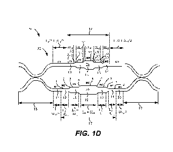
present invention
utilize a first waveguide with differing widths. The inventors have determined
that the use of
tapered regions, also referred to as taper portions, in one waveguide, but not
the other
waveguide, may introduce phase differences or phase imbalance between the two
waveguides.
Accordingly, in some embodiments, each waveguide includes all waveguide widths
with
tapered regions joining waveguide sections with differing widths. As a result,
each waveguide
has all waveguide widths present, with the first waveguide utilizing buffer
sections to
implement the differing widths. The lengths associated with the buffer
sections in the first
waveguide are added to the corresponding sections in the second waveguide to
maintain the
desired length difference (and resulting phase difference) between the two
waveguides.
Additionally, matching taper portions are present in both waveguides,
resulting in any phase
differences introduced by the presence of the taper portions being canceled
out. Thus, the
addition of all waveguide widths in both waveguides and matching taper
portions results in the
original phase difference between the waveguides being preserved while
canceling out any
phase imbalances introduced by the differing width and taper portions.
[0091] FIG. 1D illustrates a simplified plan view of an example MZI filter
including a phase-
balanced, passive compensation structure, according to an embodiment of the
disclosure.
Referring to FIG. 1D, example MZI filter 50 includes a passive compensation
structure 52 that
is phase-balanced, according to an embodiment of the disclosure. As shown in
FIG. 1D and in
comparison to FIG. 1A, MZI filter 50 includes a first waveguide 76 that,
rather than having a
uniform width between first coupler section 18 and second coupler section 19,
is characterized
22
CA 03239457 2024- 5- 28
WO 2023/101946
PCT/US2022/051212
by differing widths that correspond to differing widths of second waveguide
56. The differing
widths of first waveguide 76 are described in additional detail below. As a
result, embodiments
provide different waveguide widths as appropriate to compensate for
manufacturing variation,
with each different width present in each waveguide and matching taper
portions in each
waveguide.
[0092] Second waveguide 56 includes a compensation portion 17 positioned
between first
coupler section 18 and second coupler section 19. Compensation portion 17
includes a first
compensation section 1 having a second width 10, a second compensation section
3 having a
third width 11 and a third compensation section 5 having a fourth width 12. In
some
embodiments, fourth width 12 is greater than third width 11 and the third
width is greater than
second width 10. In some embodiments, the width and length of each
compensation portion
can be determined using one or more compensation equations, as described in
more detail
below.
[0093] In some embodiments, compensation portion 17 is symmetric along second
waveguide 56 and further includes a fourth compensation section 7 having third
width 13 and a
fifth compensation section 9 having first width 16.
[0094] In the embodiment illustrated in FIG. 1D, compensation structure 52 may
also include
a buffer portion 47 positioned within first waveguide 76. Buffer portion 47
positioned between
first coupler section 18 and second coupler section 19 includes a first buffer
section 31 having
second width 10 (i.e., W2), a second buffer section 33 having third width 11
(i.e., W3) and a
third buffer section 35 having fourth width 12 (i.e., W4). In the embodiment
illustrated in FIG.
1D, buffer portion 47 is symmetric along first waveguide 76 and further
includes a fourth
buffer section 37 having third width 13 and a fifth buffer section 39 having
first width 16.
[0095] In various embodiments, one or more taper portions can be positioned in-
between
each compensation section and each buffer section to transition between
different waveguide
widths. For purposes of clarity the taper portion between the waveguide
sections with first
width 15 (i.e., W1) and first buffer section 31 in first waveguide 76 and
first width 15 (i.e., W1)
and first compensation section 1 in second waveguide 56 are not shown.
Referring to first
waveguide 76, first taper portion 32 and second taper portion 34 are
illustrated between first
buffer section 31 and second buffer section 33 and between second buffer
section 33 and third
23
CA 03239457 2024- 5- 28
WO 2023/101946
PCT/US2022/051212
buffer section 35, respectively. Similarly, in this symmetric configuration,
third taper portion
36 and fourth taper portion 38 are illustrated between third buffer section 35
and fourth buffer
section 37 and between fourth buffer section 37 and fifth buffer section 39,
respectively. As
discussed above, in some embodiments, first waveguide 76 can also include one
or more taper
portions to transition widths between first coupler section 18 to first
waveguide 76 and from the
first waveguide to second coupler section 19.
[0096] Referring to second waveguide 56, first taper portion 2 and second
taper portion 4 are
illustrated between first compensation section 1 and second compensation
section 3 and
between second compensation section 3 and third compensation section 5,
respectively.
Similarly, in this symmetric configuration, third taper portion 6 and fourth
taper portion 8 are
illustrated between third compensation section 5 and fourth compensation
section 7 and
between fourth compensation section 7 and fifth compensation section 9,
respectively. As
discussed above, in some embodiments, second waveguide 56 can also include one
or more
taper portions to transition widths between first coupler section 18 to second
waveguide 56 and
from the second waveguide to second coupler section 19.
[0097] In some embodiments, each compensation section 1, 3, 5, 7, 9 of
compensation
portion 17 and each buffer section 31, 33, 35, 37, and 39 of buffer portion 47
may have a
substantially constant width. More specifically, in some embodiments, first
compensation
section 1 has a constant second width 10, second compensation section 3 has a
constant third
width 11, third compensation section 5 has a constant fourth width 12, fourth
compensation
section 7 has a constant third width 13, and fifth compensation section 9 has
a constant second
width 14. Moreover, first buffer section 31 has a constant second width 10,
second buffer
section 33 has a constant third width 11, third buffer section 35 has a
constant fourth width 12,
fourth buffer section 37 has a constant third width 13, and fifth buffer
section 39 has a constant
second width 14.
[0098] In some embodiments, each compensation section can have a particular
length, as
determined by one or more compensation equations, described in more detail
below. In order
to provide a consistent phase shift between compensations sections in first
waveguide 76 and
buffer sections in second waveguide 56, the taper portions are designed to be
consistent
between both waveguides. Thus, first taper portion 2 and first taper portion
32 are the same,
24
CA 03239457 2024- 5- 28
WO 2023/101946 PCT/US2022/051212
second taper portion 4 and second taper portion 34 are the same, etc. Thus,
any phase shift due
to light propagating through the taper portions is equal in both the
compensation sections and
the buffer sections. Additionally, any variation in the taper portions
resulting from
manufacturing processes is reduced or minimized by utilizing identical tapers
in both
waveguides.
[0099] Referring to FIG. 1A, as light propagates between first coupler section
108 and
second coupler section 110, first waveguide 104 is characterized by a first
length 106 and
second waveguide is characterized by a length equal to the sum of second
length 146, third
length 148, fourth length 150, fifth length 152, and sixth length 154 along
with the lengths of
the taper portions between compensation sections. In FIG. 1D, in order to
implement a phase
difference between the waveguides based on differences in lengths, for first
waveguide 76, the
length of the portion of first waveguide 76 adjacent first coupler section 18
with first width W1
is Li/2 + 6Li/2 and the length of the portion of first waveguide 76 adjacent
second coupler
section 19 with first width W1 is Li/2 + 6L1/2. For second waveguide 56, the
length of the
portion of second waveguide 56 adjacent first coupler section 18 with first
width 15 is 6L1/2,
and the length of the portion of second waveguide 56 adjacent second coupler
section 19 with
first width 16 is oL1/2. As shown in Table 1, the length of the buffer
sections is added to the
corresponding compensation section in order to eliminate any phase imbalance
that would
otherwise be introduced by the buffer sections. The length of each taper
portion is the same as
discussed above and the lengths of the buffer sections and the compensation
sections are:
Waveguide Buffer Section Length Waveguide Compensation Length
Section
First 31 61-2 Second 1 L2 + 61,2
First 33 6L3 Second 3 L3 + 6L3
First 35 6L4 Second 5 L4 + 6L4
First 37 61-3 Second 7 L3 + 6L3
First 39 6L2 Second 9 L2 + oL2
CA 03239457 2024- 5- 28
WO 2023/101946
PCT/US2022/051212
[0100] Accordingly, in comparison with the embodiment illustrated in FIG. 1A,
the
embodiment illustrated in FIG. 1D increases the length of the portions
adjacent first coupler
section 18 and second coupler section 19 by 6L1/2 and each compensation
section in the second
waveguide by 6L2, 6L3, and 6L4, respectively, in order to increase the lengths
by the lengths of
the buffer sections in the first waveguide as well as providing taper portions
that can be
consistent between both waveguides. Accordingly, the net phase difference
corresponding to
the length difference between Li and (L2 + L3 L4) is achieved, but with
reduced or no impact
resulting from the presence of the buffer sections and the taper portions. The
lengths of the
buffer sections introduced into first waveguide 76 and added to the
compensation sections in
second waveguide 56, i.e., 6Li, 6L2, 6L3, and 6L4 can be the same or
different. In some
embodiments, the length of the buffer section is a fraction, for example, ¨1%
of the lengths Li,
L2, L3, or L4.
[0101] FIG. 2 illustrates a single stage of a three-waveguide cascaded third
order MZI-based
filter 200 using a solution to Equation (8). Each stage can be incoherently
cascaded as shown
in FIG. 3 that illustrates an incoherently cascaded third-order MZI filter 300
having four stages
305, 310, 315, 320.
[0102] Although FIG. 2 illustrates a cascaded third order MZI-based filter in
which one of
the waveguides in each MZI filter has a constant width, the MZI filter
illustrated in FIG. 1D
can be utilized in cascaded implementations, with both waveguides having
differing widths.
As an example, the MZI filter illustrated in FIG. 1D can be cascaded with a
version of the MZI
filter illustrated in FIG. 1D, but with all of the lengths Li, L2, L3, and L4
doubled.
[0103] In some embodiments, it may be considered that the above set of
equations do not
consider loss or extinction ratio thus it may be possible that the obtained
lengths from the above
set of constraints violate the parameters of the extinction ratio.
[0104] In some embodiments, the use of more or less than N + 1 waveguide
widths can be
used. In either case, the problem is modified to an optimization problem, i.e.
a solution to
min(MX ¨ B) is desirable.
[0105] In some embodiments, the transitions in waveguide widths may not
considered
because the waveguide widths may be marginally different and therefore the
transition lengths
26
CA 03239457 2024- 5- 28
WO 2023/101946
PCT/US2022/051212
between these may not be relatively large, approximately 1 micron, in one
embodiment. This
can be relatively smaller than the length of one of the arms, for example,
approximately 100
microns, in one embodiment.
[0106] The discussion above disclosed an approach to make the MZI' s tolerant
to sources of
perturbation. The next section discloses a design process including an
approach to test the
statistical performance of an MZI device.
[0107] The first step is to define the geometry of the device and obtain
refractive indices of
waveguides as functions of w, Ii, T ... and other variables for various
angular frequencies co. In
some embodiments, this can be accomplished using commercial mode solvers. Upon
obtaining
this information, it can be stored in the form of look-up tables. To simplify
storing the spectral
dependencies, the refractive index data can be fit as follows and the
coefficients n, an/
aw, 02 n/ co2 can be stored yielding Equation (9).
an(xõ, . . . x-,õ) a2n(xi, . . x
N)
n(c.o, X1. . XN) = n(c.00, X1. . XN) + (60 w0) +
(co ¨ co0)2
aw2
(Eq. 9)
[0108] Equation (8) can then be solved to obtain various ratios xi. If an
exact solution cannot
be obtained, variation of the central resonant wavelength AA, can be minimized
for given
standard deviations in perturbation sources axi according to Equation (10).
8n1 vN-F2 arii
Z,L=2 lax
AA, =
_____________________________________________________________________________
(Eq. 10)
-z1L-'-,2KTIq
[0109] The value of L1 can be determined using Equation (3). The second MZI in
the third-
order MZI will can possess L'1 = 2L1 but the same values of Ki. Using the
obtained values of
Li, the values of t1, t2, t3 may be optimized as well as a number of stages N
to meet the
specifications of extinction ratio, transmission loss and extinction
bandwidth. In some
embodiments, extinction bandwidth (B W) may be larger than the central
wavelength shift AA,,
e.g. BW >> AA,. A Monte-Carlo analysis of the system can be performed by
repeating a
relatively large number (RN) of random simulations. The sampling can be
conducted with
knowledge of correlations in a representative fabrication process. In sonic
embodiments, the
process can be repeated until a favorable yield is obtained.
27
CA 03239457 2024- 5- 28
WO 2023/101946
PCT/US2022/051212
[0110] In some embodiments, numerical methods can be used to develop a MZI
filter. The
output of a filter can obtained using transfer matrices. A cascaded third-
order filter can include
directional couplers and the propagation of light in the two arms. A filter
can be defined to be
third-order when two asymmetric MZI's of differential length AL and 2AL are
cascaded
coherently. The transfer matrices for directional couplers and MZI arms are
shown in Equation
(11).
M = [-1K t -ix] m = a" richmarn 0]
(Eq. 11)
cPm- 0 1
[0111] In Equation (11), I t12 is the transmission coefficient of the
directional coupler.
Notably, K = 171 ¨ t12 while 0, (r = 1, 2) corresponds to the differential
phase in each of the
two asymmetric MZ1's that constitute a cascaded third-order filter. am =
e¨rot'/2
correspond to the additional losses that accrue due to the differential length
in each MZI, while
a = e_'1/2 is the common absorption experienced by the nominal length L of the
MZI arms.
For the general multi-waveguide case, L = min(Li, EiKiLi) and AL = ILi ¨
EiKiLi I. Note
that a' is the absorption coefficient in units of 1 / meter.
[0112] Upon utilizing the above transfer matrices the following expressions
for the elements
Hink of the overall transfer matrix of the cascaded third-order filter was
obtained. A single
third-order filter can be defined by three couplers with corresponding
parameters t1, t2, t3 and
two phase and absorption terms 0,, ar, where r = 1,2 as shown in Equations
(12a), (12b), (12c)
and (12d).
(co) = a[¨Ki(co)(t2(co)K3(w) + a2K2(co)t3(w)e-102(')) ¨
alti(co)e- jc51"(K2(co)K3(co) ¨ a2t(co)t3(w)e-i02")]
(Eq. 12a)
142(60) = a [
(w) (K3 (co) t2(w) + cr2K2(0)t3(60)e -jcP2(6")) +
jai(co)Ki(co)e- 01(w) (K2(o)K3(w) ¨ a2t(w)t3(w)e-i02")]
(Eq. 12b)
H21(co) = art, ¨ jKi(w)(t2(w)t3(60) + a2K2(60)1(3(60)e-i(P2(w)) ¨
jaiti(co)e-J01"(K2(w)t3(co) ¨ a2t2(w)K3 (w)e -J02")] (Eq. 12c)
H22 (0-) a[t1(w)(t2(w)t3(co) + a2K2(w)K3(w)e-j02(") +
28
CA 03239457 2024- 5- 28
WO 2023/101946
PCT/US2022/051212
ja1k1(w)e-j01(w)(K2(co)t3(co) + a2K 3 t2 (co)e- j02(a)))]
(Eq. 12d)
[0113] The validity Equations (12a)-(12d) can be shown by verifying that IH
(fp (C0)12
1HPP(W) 12
= 1 for q, p = 1, 2 under conditions of no loss (i.e. a' = 0). This relates to
the
conservation of energy. The transmission loss and pump-rejection ratios can be
calculated in
Equations (13a) and (13b), respectively.
= 1010910 ffoolEout,i(63)12(is(6))+Ii(to)d,a,
dB
(Eq. 13a)
Vout,2((0)12/p (63)do3)
tpump = 1000 x 10 logio -" mdB
(Eq. 13b)
[0114] In these embodiments the waveguides considered are silicon-on-insulator
(SOT) strip
waveguides, however other embodiments can use different configurations. The
material
dispersion can be based on the Palik model at room temperature. The dispersion
of the
effective index can be fit according to Equation (9). In this embodiment the
center wavelength
Ao = 27-cc/co0 = 1.55/Lm. The obtained coefficients are plotted in FIG. 4
showing the effective
index parameters as a function of waveguide width and height for a silicon-on-
insulator
waveguide. The obtained effective index is fit to Equation (9).
[0115] A full parameter sweep of the refractive index over angular frequency
co, waveguide
width (w) and thickness (h) is performed. In FIGS. 5A-5B, the derivatives are
plotted with
respect tow, h of the effective index at the wavelength A.0 = 1.55 hum.
[0116] In FIGS. 5A and 5B, the derivative On/ow is plotted. The value is
invariant with
thickness but changes dramatically with width. This indicates that waveguide
width variations
can be mitigated using this approach. On the other hand, while On/ Oh does
vary with width, it
only does so mildly; it varies more with regard to thickness. The magnitude of
change is about
four times larger than On/aw. In some embodiments, standard deviations ah of
the thickness
tend be smaller than those of the widths (see Table 2 showing parameters of
simulations),
which reduces their impact.
29
CA 03239457 2024- 5- 28
WO 2023/101946
PCT/US2022/051212
Pamrne
SraluA
Sndci
deviA.tiort o wW width (c.,c,) wri
Stand.z....td dt:.,vimk.s of wweguide. 0,5 LIM
6
Mauri.ki index Piik (fic.,ra
Ltr.ii.u.k.1.1)
'Tempel-m.11re ('P) BOOK
Alx.K.trption coeffki6-At 0,S <111.'$=rsi---I. 01
TA-ailm-riWi01/ cOre:ilkiefitz
Nlirribgr of stagr& 4:
Pimp 1il,zid idll,r difstributiom CA-
m.mia.rt with 6 Gi-fr:
Gair i.,..tioro for eadi third-mu- Mil. Stage UlletaDifillted.
Table 2: Parameters used for simulations.
[0117] Due to the relative invariance of On/Oh, with respect to w, the
strategy of using
multiple waveguide widths to mitigate variation in this parameter may not be
very efficacious
for particular applications. In principle, a solution is possible but the
lengths of arms obtained
turn out to be in the range of centimeters which can be too large for some
applications.
Therefore, in some applications that may benefit from small filter sizes, it
would be beneficial
to reduce the values of ch.
[0118] The coupling coefficients of the directional couplers can be determined
by obtaining
the even and odd modes of the coupled waveguide system. The coupling length
can then be
determined according to Equation (14).
tn,(co) = sin rAn(6))4 sin-1 (tin (coo))1
(Eq. 14)
LAn(a)0)A
[0119] The statistical performance of standard cascaded third-order filters is
examined to
estimate the yield for such devices. In this approach a Monte-Carlo
calculation was employed.
Waveguide widths and thicknesses were chosen at random and their effective
indices are
obtained from the previously generated look-up tables. Similarly, the
effective super-mode
indices of the couplers are obtained. The coupling coefficients are then
calculated using
Equation (14) and the parameters from Table 2 are used. The standard
deviations for
waveguide width um, = 3 nm and thickness al, = 0.5 nm are plotted in FIG. 6
showing
statistical distributions of effective index nor.
CA 03239457 2024- 5- 28
WO 2023/101946
PCT/US2022/051212
[0120] In this embodiment the entire dispersion curve has been shifted. The
distribution of
effective indices is slightly asymmetric. Therefore, in assuming a 3 nanometer
waveguide
width standard deviation and 0.5 nanometer standard deviation in thickness,
this example
evaluates variations more germane to die-to-die or intra-die variations.
Therefore, a relevant
parameter may be the critical dimension uniformity (CDU).
[0121] The overall performance for a N = 4 stage, incoherently cascaded third-
order filter
can then be obtained. The design described above had the goal of meeting the
specifications
for a pump rejection filter, that can be, in one example, 120 dB of rejection
and 50 mdB of
loss. However, from FIG. 7 that shows the statistical behavior of cascaded
third-order MZF s
without mitigation mechanisms, it can be seen that the mean rejection ratio
has shifted to
approximately 60 dB and the mean absorption coefficient has shifted to
approximately
1800 mdB, however these may have different values in other embodiments.
[0122] In one embodiment, a fabrication tolerant MZI design uses asymmetric
widths for
each MZI arm. In this particular embodiment it is desired to mitigate
variations to both
thickness (h) and width (w), so the quantity in Equation (10) is minimized.
The results are
plotted in FIG. 8 that illustrates designs to minimize susceptibility to
fabrication errors. The
minimization procedure yields a value of AA, 700 pm at various values of K for
varying
values of w1 and h = 220 nm. Incidentally, the minimization yields onaow ¨
an2/aw = 0,
while being at the mercy of o-hlonjah ¨ on2/ oh I. Therefore, in some
embodiments, o-h
should be reduced.
[0123] As shown in FIG. 9, the statistical distribution of cascaded third-
order s with
asymmetric widths w1 = SOO nm and w2 = 540 nm, h = 220 nm are illustrated. In
some
embodiments, this value can be reduced by increasing the height of the
waveguides. For
instance at h = 245.5 nm, AA, 580 pm. However, it also appears that using
thicker
waveguides in some embodiments causes the transmission loss to increase due to
dispersion.
Therefore, over engineering this aspect of the system may not be worthwhile
for some
embodiments. Using such a configuration, FIG. 9 illustrates the performance
for N = 4
incoherently cascaded third-order filters. An improvement in performance
compared to that
depicted in FIG. 7 is evident with the mean rejection ratio shifting to 110 dB
and mean loss
shifting to 188 mdB.
31
CA 03239457 2024- 5- 28
WO 2023/101946
PCT/US2022/051212
[0124] Furthermore, if coupler variations with respect to fabrication
uncertainties (simply
referred to as coupler variations henceforth) are ignored, then the
performance is shown in FIG.
illustrating the statistical distribution of cascaded third-order MZI' s in
the absence of
coupler variations with respect to fabrication uncertainties. The rejection
ratio shifts to 154 dB,
5 while the transmission loss changes to 165 mdB. In some embodiments, this
can indicate that
coupler variations predominantly produce vertical movements in the spectral
response while
the index changes produce mainly horizontal shifts. Horizontal shifts affect
both rejection ratio
and transmission loss, while vertical shifts predominantly affect rejection
ratios.
[0125] In some embodiments, while using asymmetric arms can make I and Ow ¨
10 an.2/d w I = 0, it may not correlate to a transmission minimum located
at A.0 = 1.55 tim. In the
above embodiments, it is fortuitous that for K SK, the above resonance
condition is satisfied.
Here, Sic is a relatively small amount of adjustment imparted to K. Therefore,
there may be a
residual error of ¨5ican.2/aw, which is may be undesirable. However, if two
additional
waveguide widths are used (i.e. w2, w3), then some embodiments may have
improved results.
This is demonstrated in FIG. 11, where one of the arms contains two widths of
0.5, 0.66
microns. More specifically, FIG. 11 illustrates the statistical distribution
of MZI properties for
three waveguide widths Li=22.96 tm, m=58,Ki=[1,4.2805,-4.6974] and wi =
[0.5,0.56,0.66]
microns. In this embodiment, the design can be constrained to satisfy a
condition for
transmission minimum at A0 (Equation (1)), FSR (Equation (3)) and
insensitivity to width
variations (Equation (5)).
[0126] In FIG. 11, coupler variations are neglected, building on the results
from FIG. 10. As
can be seen, there is an additional 10 dB improvement in rejection ratio,
while an improvement
in transmission loss by approximately 70 mdB. While thickness variations may
not be
mitigated using this approach since On/ Oh is not a function of w, the
additional constraint of
having a 2 0a WaCO = 0 may be included, which yields the performance in FIG.
12 showing the
statistical distribution of an MZI filter with four waveguide widths. L1 =
25.51 microns, Ki =
11,4.1464, ¨4.5875, 0.16621 and wi = 10.5, 0.56,0.66, 0.76] microns. The shape
of the
distribution appears to change, although improvements in mean values do not
appear to occur.
[0127] In principle, compensation for perturbations in w, h can be
simultaneously achieved
by choosing arms with different w, h as shown in Equation (15).
32
CA 03239457 2024- 5- 28
WO 2023/101946
PCT/US2022/051212
,w
l = lw h
ow 1,h ow 2, 2
an, an2
,1,w, h I h2
(Eq. 15)
an an 2
[0128] This results in a value of AA., = 26 pm. The results are plotted in
FIG. 13 illustrating
fabrication tolerance achieved using asymmetric widths as well as heights.wi =
500 nm, w2 =
535 nrn, hi = 220 nanometers and 17.2 = 245 nanometers. The average pump
rejection shifts
to 174 dB and the average loss is 125 mdB, which is smaller compared to the
case when only
asymmetric widths without coupler variations (FIG. 10) are considered. Here,
too the effect of
coupler variations have been ignored. The marginal increase in absorption
relative to FIGS. 11
and 12 is that the constraint of fixing A, is not satisfied. In some
embodiments, waveguide
geometries that effectively enable different heights (such as rib waveguides)
can be used.
Furthermore, some embodiments can use both different heights and multiple
widths to further
improve performance.
[0129] While obtaining different thicknesses can be challenging in some
embodiments, there
may be ways to accomplish this by using unconventional cross-sections that are
compatible
with current CMOS-foundry processes, as shown in FIGS. 14A-14D. In one example
embodiment shown in FIG. 14A, a conventional strip waveguide is shown. In FIG.
14B, a
cross-section which has an additional silicon nitride or silicon layer on top
of the SOI strip
waveguide that modifies the effective height is shown. FIG. 14C illustrates a
rib waveguide
and FIG. 14D illustrates a modified rib waveguide showing two other
embodiments that offer
height changes.
[0130] The effect of coupler dispersion and insertion loss on the system can
now be
considered. All the systems are assumed to possess the three-waveguide design
from FIG. 11,
however other embodiments may have other configurations. In the first
embodiment illustrated
in FIG. 15, the coupler dispersion is retained while waveguide loss is reduced
to 0.1 dB/cm.
FIG. 15 illustrates performance of the filter when the loss is reduced to 0.1
dB/cm and with
couplers robust to fabrication variations but with varying transmission with
respect to
frequency.
33
CA 03239457 2024- 5- 28
WO 2023/101946
PCT/US2022/051212
[0131] With this improvement, the transmission loss has reduced to 93 mdB,
while the pump
rejection has been minimally altered. On the contrary, when the loss is
maintained at 0.3 dB/cm
but the couplers are fab-tolerant and also not dispersive, the transmission
loss falls below the 50
mdB level as shown in FIG. 16. FIG. 16 illustrates performance of the filter
when the loss is 0.3
dB/cm with couplers that are robust to fabrication variations and also with
constant
transmission with respect to frequency.
[0132] Thus, in order to meet device specifications, in some embodiments, the
couplers may
be fab-tolerant and broadband. When the loss is also reduced to 0.1 dB/cm with
couplers robust
to fabrication and also with constant transmission coefficients with respect
to frequency,
transmission losses reduce to 28 mdB as can be seen in FIG. 17. FIG. 17
illustrates
performance of the filter when loss is reduced to 0.1 dB/cm with couplers
robust to fabrication
variations and also with constant transmission with respect to frequency. In
order to reduce
transmission loss values below 25 mdB, the number of stages may be reduced to
three,
although this may also reduce the mean pump rejection ratio. Therefore, in
order to further
improve the yield, improved process control or reduced values of aw, o-h may
be needed.
[0133] As described above, the variations of width and thickness were treated
as independent
random variables and each stage was assumed to vary independently. In this
section the case
when the width and height variations are uncorrelated but all stages are well-
correlated is
evaluated. When the correlation between each stage increases, the spread in
performance
increases as shown in FIG. 18. FIG. 18 illustrates asymmetric widths where
width and height
variations are independent and every stage is correlated with a loss of 0.3
dB/cm.
[0134] However, in some embodiments, if the couplers are made insensitive to
fabrication,
then the performance improves as seen in FIG. 19. FIG. 19 shows an embodiment
having
asymmetric widths where width and height variations are independent and each
stage is
correlated. Couplers are considered fabrication tolerant and the loss is 0.3
dB/cm. Using three
or four waveguide widths, as was the case in FIGS. 11 and 12, improves
performance even
more, bringing elements close to specifications in FIG. 20. FIG. 20
illustrates an embodiment
where width and height variations of every stage are correlated. In additional
to mitigating
coupler variations, one embodiment uses three waveguide widths. The waveguide
loss assumed
in this embodiment is 0.3 dB/cm.
34
CA 03239457 2024- 5- 28
WO 2023/101946
PCT/US2022/051212
[0135] If develop broadband couplers are developed while maintaining loss at
0.3 dB/cm, the
performance improvement is line with trends in the previous embodiments, as
shown in FIG.
21. FIG. 21 illustrates an embodiment where width and height variations are
independent but
are correlated for all stages. The structure uses three waveguide widths and
fab-tolerant and
broadband couplers and the insertion loss is 0.3 dB/cm. As illustrated in FIG.
22, the loss is
reduced to 0.1 dB/cm, which brings the performance to similar levels as shown
in FIG. 17.
More specifically, even when the correlations are not favorable, the devices
have comparable
yield. FIG. 22 illustrates an embodiment where width and height variations are
independent
but are correlated for all stages. The structure uses three waveguide widths,
fab-tolerant and
broadband couplers as well as a reduced insertion loss of 0.1 dB/cm.
[0136] Serial improvements are summarized that can be achieved for various
design
improvements shown in Table 3. In some embodiments, broadband, fabrication
insensitive
couplers enable the system to meet performance specifications. In further
embodiments,
reducing waveguide losses on-chip may help improve the performance and yield.
In addition
embodiments having o-, <3 nanometers and o-h < 0.5 nanometers may be used.
[0137] Table 4 summarizes different embodiments that may have reduced
performance and
also identifies various strategies that could potentially address the
performance. Each point
labelled (i)-(iv) in Table 4 is discussed in more detail below.
[0138] (i) In some embodiments, the use of asymmetric arm widths may achieve
tuning-free
operation of cascaded third-order filters. Use of three or four waveguide
widths helps achieve
pinning the transmission minimum and also compensates 02n/aw5co.
[0139] (ii) In some embodiments, the use of multi-waveguide sections can
mitigate many
sources of variation but due to the invariance of an/3h to w, this approach
may need long
device lengths to mitigate thickness variations. In principle, using different
waveguide heights
can also address thickness variation issues, although this may not be a CMOS-
foundry
compatible process. Some embodiments may use unconventional waveguide
geometries to
effectively engineer a height difference.
CA 03239457 2024- 5- 28
WO 2023/101946
PCT/US2022/051212
Design Mean Pump 11 - > 120 Mean
tth,, + < 25 mdB
rejection Opurap(dB) dB(%) Transmission oi. (%)
pump (dB) loss (mdB)
(mdB)
Standard third-order, 4 stage MZI, 60 44 0 1830
3074 0
0.3 dB/cm
Asymmetric widths, 0.3 dB/cm 110 92 28 188
280 0
Asymmetric widths and robust 154 130 87 164
237 0
couplers, 0.3 dB/cm
Multiple widths, robust couplers, 0.3 163 97.4 99.4 110
155.1 0
dB/cm
Standard third-order, 4 stage MZI, 163 98.2 99.43 44
80 2.2
0.3 dB/cm
Multiple widths, robust couplers and 163 143.5 97.1 93
144.1 0
0.1 dB/cm loss
Multiple widths, robust and 163 141.5 97.4 28
67 67.3
broadband couplers and 0.1 dB/cm
loss
Multiple widths, robust couplers and 122 104 55.1 22
56 76.2
0.1 dB/cm loss, 3 stages
ow = 1 nm, oh = 0.25 nm and Multiple 188 175 100 10.5
12.5 99.7
widths, robust, broadband couplers,
0.1 dB/cm,4 stages
ow - 1 nut, uh - 0.25 nm and Multiple 141 131 98.5 7.8
8.8 100
widths, robust, broadband couplers,
0.1 dB/cm,3 stages
Asymmetric widths, correlated stage 111 73.26 36 210
609 0
variations, 0.3 dB/cm
Asymmetric widths, robust couplers 148 102 69 178
329.3 0
and correlated stage variations, 0.3
dB/cm
Multiple widths, robust couplers and 164 123 78 105
177 0
correlated stage variations, 0.3 dB/cin
Multiple widths, robust and 163 120.75 80 44
103 21
broadband couplers and correlated
stage variations, 0.3 dB/cm
36
CA 03239457 2024- 5- 28
WO 2023/101946
PCT/US2022/051212
Design Mean Pump 11 ¨ > 120 Mean
jnõs + < 25 mdB
rejection CYpump(dB) dB(%) Transmission moss (%)
jtpump (dB) loss (mdB)
(mdB)
Multiple widths, robust and 163 120 78 28
95 79
broadband couplers and correlated
stage variations, 0.1 dB/cm
iaw = mm, Oh- 0.25 nm and Multiple 187 163 99.2 10.5
13.85 99.4
widths, robust, broadband couplers,
0.1 dB/cm, correlated
oaw = 1 nm,451, = 0.25 nm and Multiple 141 124 91 7.8
10.38 99.6
widths, robust, broadband couplers,
0.1 dB/cm,3 stages
Table 3
Frr)blere Reason Value Stratege
(1) Resonark.e shift
Multiple watreguid.e widths
(.0 Sens.sitivity to height Equal heights SI¨Si02¨Si,
watreguidEz
Tramnimnon loss Thsparsion in c-,ouplers & redB Broad band
non pi em
Om) Bandwidth of filter 1.e.11-.41 ntri at -160 dB Red:v:4cl
wevweide loix;
Additional stages c;r alternate arolliteattrea,
Table 4
[0140] As shown in FIG. 23, in some embodiments, reducing o- to 1 nanometer
and o-h to
0.25 nanometer from 3 and 0.5 nanometer respectively enables the
specifications to
comfortably meet the goals.
[0141] (iii) In some embodiments, the role of coupler dispersion and
variations with
fabrication may be important. Designing couplers that are more broadband and
insensitive to
fabrication variations may be needed to make a filter robust to perturbations.
[0142] (iv) In some embodiments, to meet specifications, loss may reach
approximately 0.1
dB/cm. This may enable specifications to be exceeded by adding further
cascaded third-order
MZ1 filter stages. In further embodiments, using three stages may meet
rejection ratio targets
while keeping losses below the 25 mdB level.
37
CA 03239457 2024- 5- 28
WO 2023/101946
PCT/US2022/051212
[0143] (v) In some embodiments, further improvement of fabrication tolerances
to aw <<
3 nm and ah << 0.5 nanometer may improve the mean pump rejection to 188 dB and
average
loss to 10.54 mdB for a four stage cascaded third-order MZI as is seen in
FIGS. 23A and 23B.
[0144] FIG. 24 illustrates yield percentage of loss < 25 mdB and rejection
ratio > 120db.
Variations are correlated, with insertion loss of 0.1 dB/cm, broadband and fab-
tolerant couplers
and multiple waveguide width arms.
[0145] Although MZI filter 100 (see FIG. 1) is described and illustrated as
one particular
type of MZI-based photonic device, a person of skill in the art with the
benefit of this
disclosure will appreciate that compensation structures as described above are
suitable for use
with myriad other MZI-based photonic devices. For example, in some embodiments
the MZI
passive compensation structures disclosed herein can be implemented in MZI-
based photonic
switching devices, as described in more detail below.
[0146] FIGS. 25 and 26 show example MZI-based photonic switches 2500 and 2600,
respectively, that include one or more variable phase-shifters and can also
include one or more
compensation structures. Photonic switches 2500 and 2600 are similar to MZI
filter 100 (see
FIG. 1), each having two parallel waveguides (2510a, 2510b in FIG. 25, and
2610a and 2610b
in FIG. 26), however photonic switches 2500 and 2600 each include one or more
phase shifters
(2505a, 2505b, 2505c in FIG. 25 and 2605 in FIG. 26) disposed in one or more
waveguides of
each photonic switch. Phase-shifters (2505a, 2505b, 2505c in FIG. 25 and 2605
in FIG. 26)
can be implemented a number of ways in integrated photonic circuits and can
provide control
over the relative phases imparted to the optical field in each waveguide. In
some embodiments,
variable phase-shifters can be implemented using thermo-optical switches.
[0147] In some embodiments thermo-optical switches can use resistive elements
fabricated
on a surface of the photonic device. Employing the thermo-optical effect in
these devices can
provide a change of the refractive index n by raising the temperature of the
waveguide by an
amount of the order of 10-5K. One of skill in the art having had the benefit
of this disclosure
will understand that any effect that changes the refractive index of a portion
of the waveguide
can be used to generate a variable, electrically tunable, phase shift. For
example, some
embodiments can use beam splitters based on any material that supports an
electro-optic effect.
38
CA 03239457 2024- 5- 28
WO 2023/101946
PCT/US2022/051212
In some embodiments so-called x(2) and x(3) materials can be used such as, for
example, lithium
niobate, BBO, KTP, BTO, and the like and even doped semiconductors such as
silicon,
germanium, and the like.
[0148] In some embodiments, switches with variable transmissivity and
arbitrary phase
relationships between output ports can also be achieved by combining
directional couplings
(e.g., directional couplings 2515a, 2515b in FIG. 25 and 2615a, 2615b in FIG.
26), and one or
more variable phase-shifters (e.g., phase-shifters 2505a, 2505b, 2505c in FIG.
25 and 2605 in
FIG. 26) within each photonic switch. Accordingly, complete (e.g., analog or
digital) control
over the relative phase and amplitude of the two output ports can be achieved
by varying the
phases imparted by phase shifters (2505a, 2505b, 2505c in FIG. 25 and 2605 in
FIG. 26). FIG.
26 illustrates a slightly simpler example of a MZI-based photonic switch that
allows for
variable transmissivity between ports 2620a and 2620b by varying a phase
imparted by phase
shifter 2605.
[0149] In some embodiments one or more compensation structures can be
implemented
within MZI-based photonic switches 2500,2600 using compensation equations
similar to those
described above with regard to MZI filter 100 (see FIG. 1). More specifically,
the
compensation equations can be used to determine a width and a length of each
compensation
portion that can be used to reduce a shift in frequency response caused by
various
perturbations, including variations in manufacturing widths of the waveguides,
manufacturing
variations in thicknesses of the waveguides and variations in temperature.
Similar to the
compensation structures described for MZI filter 100 (see FIG. 1),
compensation structures can
be employed in one or more waveguides (2510a, 2510b in FIG. 25, and 2610a and
2610b in
FIG. 26), and each compensation structure can each have a quantity of
waveguide widths that is
greater than the number of perturbations, however the governing equations may
be different for
an MZI-based photonic switch embodiment, as described in more detail below.
[0150] The phase relationship in an MZI-based photonic switch embodiment may
be
described as follows. The first two terms can be the same as MZI filter 100
(see FIG. 1),
however a third term corresponding to a sum of various index changes, Anj,
weighted by
various overlap integrals F3, can be added, as described by Equations (16) and
(17).
39
CA 03239457 2024- 5- 28
WO 2023/101946
PCT/US2022/051212
(2171+1)11 ¨ n1 (WO)L1 ¨ EiKiLini(wo) +Eiri(coo)Ani(wo)Li (Eq. 16)
2
c
(Eq. 17)
VFSR = Li(nfli_zingoci)
[0151] The corresponding compensation equation for the case of an MZI-based
photonic
switch which requires invariance to width can be described by Equation (18).
acki = L1 _______ _ 0 (art, EiKiani Ejar j An) (Eq. 18)
aw aw aw aw i )
[0152] Equation (18) can be reduced to Equation (19).
ziKian, = x ari An + an,
(Eq. 19)
aw i aw J aw
[0153] In some embodiments, Equations (20) through (22) can be used to account
for
compensation of higher-order derivatives.
EiKia2ni = E a [ arl An -] 82 ni (Eq. 20)
&yaw i ao) aw i awo co
Eircia2ni = E.[d2ri An.] _a2n1 (Eq. 21)
aw2 J aw2 J ow2
(ni(cou)¨Eini(cou)Ki+Eiri(coo)Anj(wo)) (m+1-)Ao
__________________________________________________ = y =
________________________ (Eq. 22)
(nfli-zingoci) ciFsR
[0154] Generalizing to arbitrary perturbations X k, the set of compensation
equations for
MX = B can be described by Equations (23) through (25) .
Yng2 ¨ nz ylig3 ¨ n3 ... yng(N+2) ¨ nN+2
an2 an3 OnN+2
axõ ax, axi
...
an2 an3 OnN+2
M = axK axK axK (Eq. 23)
an2 an, anN+2 _
a wax, awax, awax,
===
an2 an3 8nN+2
...
_ awaxi< acoaxx acoaXK
K2 1
X ¨ [ K3
(Eq. 24)
KN +2
CA 03239457 2024- 5- 28
WO 2023/101946
PCT/US2022/051212
-yngi - n1 ¨ (coo)Ani(o)0)-
an1 E 19171 An-
ax,
an1 E ¨1 1¨ An
axõ axk
B =
(Eq. 25)
02n1 j_ aFj
acoaXõ aco axk
nj
a2n a2r
+ E- An-
ax2 ax2
[0155] For partial mitigation, the set of compensation equations for MiX = B'
can be
described by Equations (23') to (25').
-yng2 ¨ n2 yna3 _
r7/..g(N+2) ¨ nN+2
an2 an3 onN+2
¨
ax, ax, ax,
an2 an3 anN+2
Mf axK axK axK
(Eq. 23')
an2 an3 anN+2
waX, awaX, waX,
an2 an3 anN+2
_ awaxi< awaxic acoaxic
K2
X = K3 (Eq. 24')
KN+2
¨ ¨ Ejr; (coo)Anj(wo)-
(Xidan Ani)
Or
E2 Pan E An )
axõ axk
B' =
(Eq. 25')
a2n1 a r Or A \
(EN E3 VawaXic aw`v mck
.92n 82r
ax2_L1 ax2-1 Anj)
[0156] Photonic switches 2500 and 2600 illustrated in FIGS. 25 and 26,
respectively, and the
associated compensation equations are two examples of how compensation
structures can be
implemented in myriad MZI-based photonic devices. One of skill in the art with
the benefit of
41
CA 03239457 2024- 5- 28
WO 2023/101946
PCT/US2022/051212
this disclosure can appreciate that similar compensation structures can be
implemented in other
MZI-based photonic devices.
[0157] For simplicity, various components, such as the optical pump circuitry,
substrates,
cladding, and other components of MZI filter 100 (see FIG. 1) are not shown in
the figures. In
the foregoing specification, embodiments of the disclosure have been described
with reference
to numerous specific details that can vary from implementation to
implementation. The
specification and drawings are, accordingly, to be regarded in an illustrative
rather than a
restrictive sense. The sole and exclusive indicator of the scope of the
disclosure, and what is
intended by the applicants to be the scope of the disclosure, is the literal
and equivalent scope
of the set of claims that issue from this application, in the specific form in
which such claims
issue, including any subsequent correction. The specific details of particular
embodiments can
be combined in any suitable manner without departing from the spirit and scope
of
embodiments of the disclosure.
[0158] Additionally, spatially relative terms, such as "bottom or "top" and
the like can be
used to describe an element and/or feature's relationship to another
element(s) and/or feature(s)
as, for example, illustrated in the figures. It will be understood that the
spatially relative terms
are intended to encompass different orientations of the device in use and/or
operation in
addition to the orientation depicted in the figures. For example, if the
device in the figures is
turned over, elements described as a "bottom" surface can then be oriented
"above" other
elements or features. The device can be otherwise oriented (e.g., rotated 90
degrees or at other
orientations) and the spatially relative descriptors used herein interpreted
accordingly.
[0159] Various examples of the present disclosure are provided below. As used
below, any
reference to a series of examples is to be understood as a reference to each
of those examples
disjunctively (e.g., "Examples 1-4" is to be understood as "Examples 1, 2, 3,
or 4").
[0160] Example 1 is a Mach-Zehnder interferometer (MZI) filter comprising: a
first
waveguide having a first length and extending from a first coupler section
having a first width
to a second coupler section having the first width and including: a first
buffer section having a
second width; a second buffer section having a third width; a first taper
portion positioned
between the first coupler section and the first buffer section and
transitioning from the first
coupler section to the second width; and a second taper portion positioned
between the first
42
CA 03239457 2024- 5- 28
WO 2023/101946
PCT/US2022/051212
buffer section and the second buffer section and transitioning from the second
width to the third
width. The MZI filter also includes a second waveguide extending from the
first coupler
section to the second coupler section and including: a tolerance compensation
portion
positioned between the first coupler section and the second coupler section,
wherein the
tolerance compensation portion includes a first compensation section having
the second width
and a second compensation section having the third width; a third taper
portion positioned
between the first coupler section and the first compensation section and
transitioning from the
first coupler section to the second width; and a fourth taper portion
positioned between the first
compensation section and the second compensation section and transitioning
from the second
width to the third width.
[0161] Example 2 is the M_ZI filter of example 1 wherein the first buffer
section has a length
of 61_,2 and the first compensation section has a length of L2 + 6L2.
101621 Example 3 is the MZI filter of example(s) 1-2 wherein the second buffer
section has a
length of 6L3 and the second compensation section has a length of 1.3 5L3.
[0163] Example 4 is the MZI filter of example(s) 1-3 wherein dimensions of the
first taper
portion and the third taper portion are equal and dimensions of the second
taper portion and the
fourth taper portion are equal.
[0164] Example 5 is the MZI filter of example(s) 1-4 wherein the first
compensation section
has a constant second width and the second compensation section has a constant
third width.
[0165] Example 6 is the MZI filter of example(s) 1-5 wherein the tolerance
compensation
portion is symmetric and includes a third compensation section having the
second width.
[0166] Example 7 is the MZI filter of example(s) 1-6 wherein the third width
is greater than
the second width.
[0167] Example 8 is the MZI filter of example(s) 1-7 wherein the first
waveguide and the
tolerance compensation portion form components of a tolerance compensation
structure that
compensates for a variation in a width of the first waveguide and a variation
in a width of the
second waveguide due to manufacturing tolerances.
43
CA 03239457 2024- 5- 28
WO 2023/101946
PCT/US2022/051212
[0168] Example 9 is the MZI filter of example 8 wherein the tolerance
compensation
structure reduces a shift in a frequency response of the MZI filter due to the
variation in width
of the first waveguide and the variation in width of the second waveguide.
[0169] Example 10 is a method for making a Mach-Zehnder interferometer (MZI)
filter, the
method comprising fabricating a first waveguide having a first length and a
first continuous
width and fabricating a second waveguide having a second length and a
plurality of widths
along the second waveguide. The first and the second waveguides simultaneously
satisfy:
rnAo Li.(ni.(Ao) Eini(Ao)Ki)
V Fs-R = ________________________________________________
Li (no ¨ Zingiki)
ani dni
E- - = = -
j a Xi Kt d X-
62,n1 o2ni
Eq X a co = Ei __
dX- co
2ni
Eu = Zifcz
wherein:
m = an integral multiple;
L1 = a reference length of the first waveguide;
Ao= a central wavelength of light in the first and the second waveguides;
Li= a length of an ith portion of the second waveguide;
n1= a modal refractive index of the first waveguide;
ni= a modal refractive index of an ith portion of the second waveguide;
no= a group refractive index at a central wavelength/A0 for the first
waveguide;
ngi = a group refractive index at the center wavelength Ao;
Ki = L1/ L1;
VF5-R = free spectral range;
c = speed of light;
44
CA 03239457 2024- 5- 28
WO 2023/101946
PCT/US2022/051212
Xj= a number of sources of perturbation;
co= angular frequency;
Xi= a waveguide width;
2(2= a waveguide thickness; and
E- Eq' and Eu are compensation factors greater than zero and less than one.
[0170] Example 11 is the method of example 10 wherein Ej Eq Ezi = E.
[0171] Example 12 is the method of example(s) 10-11 wherein the second
waveguide has a
first compensation section having a second width, a second compensation
section having a third
width and a third compensation section having a fourth width, wherein the
fourth width is
greater than the third width and the third width is greater than the second
width.
[0172] Example 13 is the method of example(s) 10-12 wherein the second
waveguide further
includes: a first taper portion positioned between a first coupler section and
the first
compensation section and transitioning from the first coupler section to the
second width; a
second taper portion positioned between the first compensation section and the
second
compensation section and transitioning from the second width to the third
width; and a third
taper portion positioned between the second compensation section and the third
compensation
section and transitioning from the third width to the fourth width.
[0173] Example 14 is the method of example(s) 10-13 wherein the number of
sources of
perturbation is selected from a manufacturing tolerance variation in a width
of each of the first
and the second waveguides, a manufacturing tolerance variation in a thickness
of each of the
first and the second waveguides and a temperature variation in each of the
first and the second
waveguides.
[0174] Example 15 is the method of example 14 wherein the MZI filter is
configured to
reduce a shift in a frequency response of the MZI filter due to the sources of
perturbation.
[0175] Example 16 is a method for making a Mach-Zehnder interferometer (MZI)
filter, the
method comprising fabricating a first waveguide extending from a first coupler
section having
a first width to a second coupler section having the first width, wherein the
first waveguide has:
a first length Li;
CA 03239457 2024- 5- 28
WO 2023/101946
PCT/US2022/051212
a first buffer section having a second width;
a second buffer section having a third width;
a first taper portion joining the first coupler section and the first buffer
section; and
a second taper portion joining the first buffer section and the second buffer
section;
and
fabricating a second waveguide extending from the first coupler section to the
second coupler
section, wherein the second waveguide has:
a first compensation section having the second width;
a second compensation section having the third width;
a third taper portion joining the first coupler section and the first
compensation
section; and
a fourth taper portion joining the first compensation section and the second
compensation section;
The first waveguide and the second waveguides simultaneously satisfy:
mA0 = Li (ni (A0) ¨ Eini (A0)Ki)
VFSR = (
¨ ZingiKi)
ani ani
E--=EiK = ¨
ax, a X
azni azni
E __________________________________________ = Ei Ki __
ci a X -act) oX- GO
azni aznt
s =
it EiKi ax?
wherein:
m = an integral multiple;
A0= a central wavelength of light in the first and the second waveguides;
46
CA 03239457 2024- 5- 28
WO 2023/101946
PCT/US2022/051212
Li= a length of an th portion of the second waveguide;
n1= a modal refractive index of the first waveguide;
ni= a modal refractive index of an ith portion of the second waveguide;
no= a group refractive index at a central wavelength/A0 for the first
waveguide;
nfli = a group refractive index at the center wavelength /1.0;
Ki = Li/Li;
1/17SR ¨ free spectral range;
c = speed of light;
Xj= a number of sources of perturbation;
co= angular frequency;
Xi = a waveguide width;
X2= a waveguide thickness; and
Ei, Eq, and su are compensation factors greater than zero and less than one.
[0176] Example 17 is the method of example 16 wherein si = Eq = Su = E.
[0177] Example 18 is the method of example(s) 16-17 wherein the second
waveguide has a
first compensation section having a second width, a second compensation
section having a third
width and a third compensation section having a fourth width, wherein the
fourth width is
greater than the third width and the third width is greater than the second
width.
[0178] Example 19 is the method of example(s) 16-18 wherein the second
waveguide further
includes: a first taper portion positioned between a first coupler section and
the first
compensation section and transitioning from the first coupler section to the
second width; a
second taper portion positioned between the first compensation section and the
second
compensation section and transitioning from the second width to the third
width; and a third
taper portion positioned between the second compensation section and the third
compensation
section and transitioning from the third width to the fourth width.
[0179] Example 20 is the method of example(s) 16-19 wherein the number of
sources of
perturbation is selected from a manufacturing tolerance variation in a width
of each of the first
and the second waveguides, a manufacturing tolerance variation in a thickness
of each of the
47
CA 03239457 2024- 5- 28
WO 2023/101946
PCT/US2022/051212
first and the second waveguides and a temperature variation in each of the
first and the second
waveguides.
48
CA 03239457 2024- 5- 28