Note: Descriptions are shown in the official language in which they were submitted.
1~'715~j~
- 1 - 20104-8134
Biplane phased array transducer Eor ultrasonic medical imaging.
This invention relates to a biplane phased array trans-
ducer for ul-trasonic medical imaging comprising
a plate of a piezoelectric material with
a conductive electrode material laminated on each of the
major surfaces of said plate, forming electrode surfaces thereon,
each of said electrode surfaces being scored to provide a
matrix of transducer elements, the scoring of one e~ectrode sur-
face being at an angle to the scoring oE the second electrode
surface.
Modern ultrasound scanners employ phased array trans-
ducers to accomplish electronic steering and focussing of the
acoustic beam in a planar sector. These arrays are commonly
` fabricated from a plate of piezoelectric ceramic by cutting the
plate into narrow plank-shaped elements. In order to obtain a
wide angular response free of grating lobes, the center-to-center
element spacing is approximately a half wavelength of sound in
tissue at the center frequency.
A novel device combining two orthogonal phased arrays
for real time imaging of two orthogonal sectors is disclosed in
Canadian Patent Application Serial Number 512,472, filed June 26,
1986 (PHA 21.273). This application discloses a biplane phased
array fabricated by putting an electrode surface on each major
surface of a slice of a composite piezoelectric material and scor-
ing the electrode surfaces such that the scoring on one side is at
an angle with the scoring on the other side and the scoring does
,~
~7~Ls5~
- la - 20104-8134
not penetrate the composite materlal. Appropriate electrical
connections are made such that all electrode elements on one elec-
trode surface are grounded and the phasing is performed with re-
~ 7~L~i55
20104 813~maining free electrodes to image, accordirlg to the phased array
principle in one direction, and alternately all t,he electrode
elements on the other electrode surface are grounded so that the
phasing is performed with the free electrodes on the first side to
image in a second direction. The array of transducers is capped
on one side by a mechanical lens.
Such a biplane phased array is especially useful in
cardiac scanning. Simultaneous horizontal and vertical cross
sections of the heart will allow the physician to evaluate more
effectively the functionlng of the heart. The demonstration of
low cross talk in composite piezoelectric arrays suggested the
application of composite materials to the design of a biplane
phased array. The forming of phased arrays of transducer elements
on both of the opposed major faces of the same piece of electric
plate requires a new method of defining the transducer array
elements, because a complete cutting of the elements as was done
in the prior art of conventional phased arrays is not feasible.
In the cross referenced application, the array elements were
formed by scoring the electrode surfaces, such that the scoring on
~0 one side is at an angle with the scoring on the other side. A
composite piezoelectric material was used to reduce cross talk
between the transducer elements.
It is an object of the present invention to provide a
biplane phased array transducer of the kind degcribed in the
opening paragraph, in which cross talk between the transducer
elements is reduced even further, even i~ a homogeneous
piezoelectric material is used.
7~5~5
20104-8134
According to a broad aspect of the invention there is
provided an array transducer for ultrasonic medical imaging
comprising:
a plate of a piezoelectric material having plural major
surfaces;
a conductive electrode material laminated on each of the
major surEaces of said plate, forming electrode surfaces thereon;
each major surface of said piezoelectric plate being diced
through its electrode surface and partially through the
piezoelectric material to provide a matrix of acoustically
separated transducer elements, the partial dicing of one of said
major surfaces being at an angle to the partial dicing of the
second of said major surfaces;
means to connect alternately all electrode elements on one
major transducer surface with phased array electronics while
grounding the electrode elements o~ the other major transducer
surface to effect a sector scan alternately in each of said ~wo
planes, such that an image in one direction is followed
immedi~tely by an image in a second direction, thus produciny a
dynamic image of a bodily function.
According to another broad aspect of the invention there
is provided an array ultra~onic transducer compristng:
a plate of a composite piezoelectric ceramic material having
two major surfaces, each major surface being diced partially
through tha said composite piezoelectric ceramic material;
a plurality of adjacent electrode elements formed by said
partial dicing exposed on each of said two major surfaces~ those
2a
1~7~555
2010~-813~
electrode elements on a first surface being at an angle ~o those
electrode elements on the second surface, the portion of said
plate underlying each of said electrode elements defining a
separate transducer element;
electrical circuit means connecting lines to each of said
electrode elements such that when the electrode elemPnts on one
oiE said major surfaces are acti~le, the lines to the electrode
elements on the other major sur~Eace are grounded;
means to connect alternate:ly all electrode elements on one
electrode surface with phased array electronics while grounding
the electrode elements on the other major electrode sur~Eace to
effect alternately a sector scan in each of the t~o planes, such
that an image in one direction is followed immediately by an image
in a second direction, thus producing a nearly dynamic image o~ a
bodily function.
2b
'5'5'~:i
- 3 - 20104-8134
The invention will now be explained in detail with
reference to the drawings.
Figure la is an exaggerated perspective view of a trans-
ducer element used in a conventional phased array.
Figure lb is an exaggerated perspective view of a trans-
ducer element in the phased array of the present invention.
Figure 2 is a partially cut away perspective view of a
biplane phased array transducer formed by cross dicing of a piezo-
electric plate.
Figures 3a and 3b are diagrammatic representations of
the basic configuration for the electronics required for the
excitation of orthogonal elements in a biplane phased array.
Figure 4 is a graph showing measured radiation patterns
from a single element in a composite phased array defined by an
electrode pattern alone.
Figure 5 is a graph showing the measured radiation from
a single element in a phased array formed by cross dicing -the
composite plate to 30% of its thickness.
Figure 6 is a graph showing a measured radiation pattern
from individual elements in a biplane phased array formed by cross
dicing the composite plate to 60~ of its thickness.
Figure la is a side perspective view of a single trans-
ducer element 1 of a conventional phased array. Phased array
transducers have been traditionally employed to accomplish the
electronic steering and focussing of an acoustic beam in a planar
sector. Phased arrays are commonly fabricated from a plate of the
piezoelectric ceramic by cutting it into narrow plank-shaped ele-
LS~S
- 4 - 20104-8134
ments. In order to obtain a wide angular response free of grating
lobes, the center-to-center element spacing is approximately a
half wavelength of sound in tissue at the center frequency.
A novel device combining two orthogonal phased arrays,
for the real time imaging of two orthogonal sectors is disclosed
in Canadian Patent Application Serial Number 512,472 filed
June 26, 1986 (PHA 21.273). The biplane phased array of that
application disclosed the use of a composite piezoelectric mate-
rial having conductive electrode surfaces on both sides. In that
application the electrode surfaces are scored to define the
individual transducer array elements.
Figures lb, 2 and 3 disclose the structure of the
improved composite biplane phased array of the present invention.
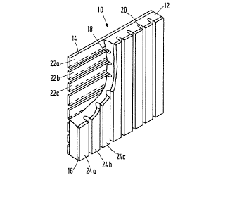
Referring first to Figure 2, the composite biplane phased array 10
of the present invention consists of a plate 12 of a composite
piezoelectric material having two conductive electrodes 14, 16 one
of such electrodes being deposited on each of the opposed major
surfaces of the plate 12. The composite piezoelectric material is
made from a matrix of parallel rods of a piezoelectric ceramic
material distributed in an electrically inert binding material
such that each of said rods is completely surrounded by the
insulating and damping material, the rods extending from one major
surface of the plate 12 to the other major surface perpendicular
to the major surfaces. Examples of the materials of this type
are disclosed in U.S. Patent No. 4,514,247 and U.S. Patent
No. 4,518,889. Such a material is also illustrated and described
in the 1984 IEEE ULTRASONIC SYMPOSIUM PROCEEDINGS, published
- 1 ~ 7~
- 4a - 20104-8134
December 19, 1984. The lateral spatial periodicity of the compo-
site piezoelectric structure is smaller than all the relevant
acoustic wavelengths. Hence, the composite behaves as a homoge-
neous piezoelectric with improved effective material parameters as
discussed in the article cited above. For purposes of discussion
electrode surface 14 will be designated the front face, while the
other electrode surface 16 will be designated the back face. When
used in an ultrasonic transducer for medical imaging, the front
face 14 is the face which is placed towards the body of the
patient.
Figure 2 is a side perspective view of the biplane
phased array transducer 10 having a plate 12 of composite piezo-
electric ceramic material, a front electrode surface 14 and a back
electrode surface 16. In the illustration of Figures 2 and 3, the
biplane phased array transducer 10 is
3L~7~L555
, ~ .
PHA 21.284 5 17.2.1986
formed by a partial cross dicing of the composite piezoelec-
tric plate 12. Channels 18 are cut in one direction on the
front through the front face electrode14 and partially into
the piezoelectric material of the plate 12 but not completely
through the plate. Channels 20 are cut through electrode
surface 16 and partially into but not through the piezoelec-
tric material of the plate 12 at an angle to channels 18. The
front electrode transducer elements 22a, 22b, 22c, ... are
obtained by this partial dicing through both the conductive
electrode surface and partially through the piezoelectric
material. Back transducer elements 24a, 24b, 24c, ... are
formed by this partial dicing through the back ~ace electrode
16 and partially through the piezoelectric material. Thus,
for this biplane phased array, the transducer elements are
formed by the partial cross dicing of the composite piezo-
electric material, in contrast to the prior art technique of
dicing completely through the piezoelectric material and
into a backing material used in the construction of con-
ventional phased arrays. While the angle of cross dicing shown
in the figures is 90, other angles may be utilized. In par-
ticular, for beam steering in a single plane the second set
of cuts can be made at varying angles.
Figures 3a and 3b are diagrammatic representations
of the basic configuration for the electronics required for
a biplane phased array. In this figure the reference 26
designates the phased array circuit responsible for exciting
the transducer elements while the reference numeral 28 re-
presents the ground connection discussed hereinafter. In a
biplane phased array according to the present invention, the
front face elements 22a, 22b, 22c, ... and the back face
elements 24a, 24b, 24c, ... are alternately connected to the
phased array circuit 26. The electronic circuits for phased
arrays are known in the art and are not discussed herein be-
cause they are not part of and essential to the invention.
The phased array circuits are designated generally by the
block 26 and they provide the means to pulse alternately all
transducer elements on one electrode surface, while grounding
.. . :
S
PHA 21.289 6 17.2.1986
the electrodes on the other electrode surface, to effect a
sector scan in two planes. In operation, either the front
face electrodes or the back face electrodes are grounded
and the phasing is performed with the remaining free elec-
trodes. This requires reversing the roles of the electrodesets 14 and 16. Thus an image in one direction is followed
quickly by an image in a second direction, producing a
dynamic image of a bodily function. Such circuits are well
known in the art and are not discussed further herein.
! 10 For n electrodes on each major surface, a total of 2n
electrodes, and 2n electrical connections are required to
operate the biplane phased array of this invention. The bi-
plane phased array, using both major surfaces oE a piezo-
electric plate, thus permits the near real time imaging of
two sector planes. In a usual application, a spherical or
at least convex mechanical lens secures focussing in a di-
rection other than that of the transducer arrays. The mecha-
nical lens may be a relatively standard lens which is made
from a material from a rather low propagation velocity.
The acoustic impedance should not be very different from
the skin acoustical impedance to suppress reverberation.
Several trial arrays of the present invention have
been tested, having a structure substantially as dis-
closed in Figures 2 and 3, namely having orthogonal arrays
on opposite faces of a composite piezoelectric plate such
that the radiation profiles from single elements of each
array are adequately broad. The results of the test summa-
rized below indicate that the purpose of the invention is
achieved with the elements formed by partially dicing the
opposite faces of the plate in orthogonal directions.
Experimental Results
This section presents the results of directivity
measurements performed on several trial arrays. The inter-
pretation of these results will be discussed separately inthe next section.
The trial devices were made from plates of rod
7~L55S
PHA 21.284 7 17.2.1986
composites (resonance frequency 3.5 MHz) in which a Stycast
epoxy holds together rods of PZT ceramic (Honeywell ~278)
oriented perpendicular to the plate face. The PZT rods had
a lateral size in the range 54-65 micron with 60 micron
spacing between the rods. Array elements (length 12-18 mm)
were formed by scribing the electrode or dicing the epoxy
between the rods so that each element included two rows of
PZT rods. Directivity measurements were performed in a
water tank in transmission and reception models using a
single resonant pulse excitation.
Undiced Arrays
The first undiced composite array ~3.3 MHz, pitch
0.23 mm) was provided with an undiced matching layer of
Mular and air cell backing. Electrical measurements of
cross talk, using a single cycle sinewave excitation,
yielded low cross coupling indexes of -26.5, -26, -29.7, and
-32 dB for the four nearest neighbours, respectively. However,
directivity measurements for a single element 1 in the array
(Fig. 1a) revealed dips near 36 degr`ees and peaks near 48 de-
grees in contrast to the expectation from the diffraction
theory for such a narrow radiator.
To investigate the origin of these phenomena a
similar array was fabricated without a matching layer and
without a backing layer. Directivity measurements for a
single element in this array revealed similar patterns with
even larger dips and peaks near 38 degrees and 48 degrees,
respectively, as shown in Fig. 4. In this Figure the rela-
tive amplitude A of the emitted radiation is plotted as a
function of the angle c~ relative to the normal in degrees.
This result indicates that the anomalies in the directivity
pattern are associated with the composite material itself.
Further experiments with undiced array ele-
ments were performed using a different composite material
made with a softer epoxy (Spurr epoxy), A 2 MHz array (pitch
0.45 mm) was formed by scribing the electrode on one face
of a Spurr/PZT composite disk. Directivity measurements for
5~:i5
PHA 21.284 ~ 17.2.1985
a single element in this array shows a broader pattern
without side l~bes. However, the measured angular beam width
is still much smaller than that expected for an isolated ele-
ment of the same dimensions.
Diced Arrays
Using the Stycast/PZT composites we tried to broad~
en the radiation pattern by partially dicing the array ele-
ments. The first experiment was conducted with a 1.2 MHz com-
posite plate. An array with a pitch of 0.65 mm was formedby dicing the elements to 30% of the plate thickness. The
radiation pattern obtained from a single element in this
- array was the same as the one obtained from an undiced ele-
ment. However, further experiments showed that a signifi-
cantly broader beam pattern is obtained when an additional
set of orthogonal cuts are made on the other face of the com-
posite plate (Fig. 2). These cross dicing experiments were
performed with 3.2 MHz composite plates. Two orthogonal
arrays with a pitch of 0O25 mm were formed by dicing the two
faces of a composite plate to 30% of its thickness. A 12 mi-
cron Kapton foil served as a face plate to keep water from
contacting the elements. The radiation profile from a single
element (Fig. 5) shows a beam width of 70 degrees at -6 dB
which is 50~ larger than that obtained with an undiced ele-
ment,
Further improvement was obtained by cross dicingthe elements to 60% of the plate thickness. Detailed directi-
vity measurements were performed with elements belonging to
the orthogonal arrays on opposite faces of the composite
3D plate. While exciting an element in the front array (facing
the water)all the electrodes on the rear face were con-
nected to the ground. In a similar way, all the electrodes
on the front face were grounded while exciting an element in
the rear array. The circles and crosses in Figure 6 show the
radiation patterns obtained from a single element in the
front array and the rear array, respectively. Both array
elements show a broad radiation pattern with an angular
1~71S55
PHA 21.28~ 9 17.2.1986
width of 96 degrees at -6 dB. This is close to the theoretical
beam width of about 100 degrees expected for an isolated ele-
ment is a soft baffle.
Discussion of Experimental Results
Undiced Arrays
The experimental results cleaxly indicate that the
anomalies in the radiation pattern from an undiced phased
array element are associated with the acoustic properties of
the composite material itself. The combination of ceramic
rods and epoxy in a composite structure creates a highly ani-
sotropicmaterial with relatively low acoustic velocities.
However, in our present Stycast/P~T composites the acoustic
velocities are high as compared to the speed of sound in
water. This velocity mismatch creates refraction effects at
the composite - water boundary which limit the angular width
of the transmitted beam.
Diced Arrays
The partical cross dicing of elements on opposite
faces of the composite plate defines two orthogonal arrays
with electrical elements divided into many mechanical sub-
elements 3 whose lateral dimensions are much smaller than a
wavelength (Fig. 1b)o These small sub-elements radiate and
receive acoustic energy at a wide angle because their lateral
dimensions are insufficient for the wave phenomena of re-
fraction to occur.
The cross dicing also prevents narrowing of the
beam due to cross talk between elements. The cross cuts
confine the acoustic path between elements to a set of very
narrc,w strips that act aswaveguides. The small transverse
dimensions of these waveguides significantly limit the num-
ber of propagating modes which they can support.
As a result of the cross dicing the sensitivity of
each array is increased because the vibration mode of each
array elements is changed from that of a width extensional
mode (or "beam mode") of a plank to that of a length ex-
~.~7~5~S
PHA 21.284 10 17.2.1986
tensional mode of a set of bars. In the Stycast/PZT compo-
sites we found that the coupling factor of an array element
is increased from 0.59 to 0.65 after 60~ in orthogonal di-
rections.
CONCLUSION
Feasibility of a biplane phased array is indicated
by the broad single-element directivity measured on a 3MHz
array formed by partially dicing the elements on opposite
face of a composite plate in orthogonal directions.
The narrow radiation profile of phased array
elements define on composites by electrode patterning alone
was shown to be due to the high acoustic velocities in the
present composite material.
The advantage of this structure of a composite
biplane phased array are as follows:
1. Sensitivity: As a result of the cross dicing,
the vibration mode of each array element is
changed from that of a width extensional mode (or
"beam mode") of a plank to that of a length ex-
tensional mode of a set of bars. The electromecha-
nical coupling factor k33 associated with the
latter is larger than that k'33 associated with
the former. For example in PZT-5, k33 = 0.705
while k 33 0.66.
2. Angular response: The cross cuts confine the
acoustic path between elements to a set of very
narrow strips that act as waveguides. The small
transverse dimensions of these waveguides signifi-
cantly limit the number of propagating modes
which they can support.The cross dicing also re-
duces narrowing of the angular response caused by
refraction effects. The small sub-elements formed
by the cross dicing can radiate and receive
acoustic energy at a wide angle because their la-
- teral dimensions are insufficient for the wave phe-
nomena of refraction to occur~
L~7~55
PHA 21.284 11 17.2.1986
3. Rigidity: The structure obtained by a partial
cross dicing is rigid and need not be supported by
a backing layer. The elimination of a backing
layer improves the sensitivity and reduces cross
coupling~
4. Versatility: The partial cross dicing technique
can be applied to the fabrication on conventional
phased arrays, bi-plane phased arrays, and two
dimensional arrays.
The cross dicing technique was tested experimental-
ly using a composite piezoelectric material. Phased arrays
(3 MHz, half-wave]ength pitch) with elements defined by an
e]ectrode pattern alone showed anomalies in the directivity
pattern for a single element as shown in Figure 4. Cross
dicing of the array elements to 30~ of the thickness of the
composite plate yielded improved results as shown in
Figure 5. Cross dicing to a depth of 60~ yielded the result
shown in Figure 6. This result agrees with the theoretical
expectation for the directivity of an isolated element in a
soft baffle.