Note: Descriptions are shown in the official language in which they were submitted.
~:~n~ 8
25307-177
BACKGROUND OF THE INVENTION
This invention relates to an active matrix display device in
which data bus lines are formed on a first transparent insulating
substrate such as a glass panel and scan bus lines are formed on a
second transparent insulating substrate, and a method for driving
the same.
More specifically, this invention concerns an active matrix
display device in which the earth bus lines on the second subst-
rate are eliminated resulting in enlarging the relative display
area per pixel (picture element) and obtaining a higher yield of
panel fabrication. Further, this invention relates to a driving
method for obtaining a high quality display, reducing a cross-talk
problem.
An active matrix display device, as well as a dot matrix type
(or so-called simple matrix type) are widley used in a display
terminal of information processing apparatus. Liquid crystal is
usually enclosed in such devices as the display medium.
In the active matrix display device, each pixel once address-
ed maintains an active state until the next scan, there~re this
type has advantages of avoiding reduction of contrast and angle of
visibility such as would happen ordinarily for the dot matrix type.
The background of the invention and the invention itself are
described with reference to the accompanying drawings in which:
Figure 1 is an equivalent circuit of an active matrix display de-
vice of the prior art;
Figure 2 is another equivalent circuit of an active matrix display
device of the prior art;
~ 25307-177
Figure 3 is an equivalent circuit and related waveforms according
to the present invention for explaining the principle of the inven-
tion;
Figure 4 is an exploded perspective view of the display device of
an embodiment of the present invention;
Figure 5 is an equivalent circuit according to the present inven-
tion for explaining a double layer bus line;
Figure 6 is a plan view of the electrode and bus line arrangement
on the second panel of the present invention;
Figures 7 through 9 are cross-sectional views taken along lines
A-A', B-B', and C-C' respectively in Figure 6;
Figure 10 is a schematic arrangement of electrodes and bus lines
of another embodiment of the present invention;
Figure 11 is a partial cross-sectional view along the scan bus line
of the structure shown in Figure 10;
Figure 12 is a plan view of the terminal configuration according
to the embodiment of Figure 10;
Figure 13 is a cross-sectional view taken along a line of V-V' in
Figure 12;
Figure 14 is an equivalent circuit for a further modification of
the present invention, wherein the drain electrode is connected to
a scan bus line through a resistor;
Figure 15 is a plan view of the electrode and bus line arrangement
of a still further modification of the present invention;
Figure 16 is an equivalent circuit for the embodiment shown in
Figure 15;
Figure 17 appearing on the same sheet as Figures 12 and 13,ShOWS the
voltage fluctuation between display electrodes for a non-addressed
2a 25307-177
~J`~6'~38
period due to impressed data pulses;
Figure 18 are waveforms during operation of the display device of
the present invention, wherein (a) shows data pulses; (b) and (c),
address pulses; (d~, source voltage; and (e), voltage between dis-
play electrodes;
Figures 19 and 20 sho~ the effects of data voltage to display el-
ectrode voltage, wherein (a) shows a data voltage waveform which
alternately reverses its polarity every horizontal scan, and (b)
shows the voltage variation of the display electrode on the second
panel due to the data voltage change;
Figure 21 shows an equivalent circuit and waveforms of address
pulses and data pulses for explaining the principle of driving
method in order to reduce uneven contrast and to obtain stable
contrast gradient;
Figure 22 s~ows the transmissivity characteristic of liquid crystal
cell as a function of applied voltage;
Figure 23 shows waveforms of data pulses, address pulses, display
electrode voltage, and voltage across display electrodes utilizing
the driving method of the present invention;
Figure 24 is a block diagram for driving`the display device`accor-
ding to the present invention; and
Figure 25 is a voltage versus time chart showing the clock signal shift
clock pulses, shift data, and address pulses of Figure 24.
3 25307-177
With reference to Figure 1, a thin film transistor (abbrevia-
ted as TFT hereinafter) 31 is used as an active switch element.
TFT 31 provides gate electrode 32, drain electrode 33, and source
electrode 34. Source electrode 34 is connected to display elect-
rode of liquid crystal display element 35. Both scan bus lines 36
and data bus lines 37 are formed on a second transparent insulating
substrate and bus lines 36 are aligned at right angles to bus lines
37.
Liquid crystal display element 35 consists of two display el-
ectrodes and liquid crystal medium held therebetween. One display
electrode is formed on the second substrate and connected to source
electrode 34 of TFT 31, and a common earth electrode formed on a
first substrate is utilized as another display electrode. Gate
electrode 32 is connected to scan bus line 36, and drain electrode
33 is connected to data bus line 37.
TFT 31, one display electrode of liquid crystal display elem-
ent 35, scan bus line 36, and data bus line 37 are formed on the
second substrate such as a glass panel, and the common display el-
ectrode is formed on the first substrate, and the two substrates
are sealed together at their peripheral regions, the substrates
are separated by a small distance apart and enclose the liquid
crystal medium.
By applying sequentially address pulses having a pulse with
such as 30 to 60 ~s, the scan bus line 36 and applying data pul-
ses to each data bus line 37 synchronized with the above address
puLse, the information is thus transmitted to each liquid crystal
display element 35 arrayed in a row and is maintained for a sub-
sequent one ~rame period.
~ 3~ 25307-177
Next, the above performance is explained in more detail. When
the scan bus line 36 is addressed, because gate electrode 32 is
connected to said scan bus line, TFT 31 is turned on, and thus da-
ta voltage is impressed to liquid crystal display element 35 thr-
ough data bus line 37 and TFT 31, and the electro-static capacitan-
ce of liquid crystal display element 35 is charged up. The above
liquid crystal display element can maintain the information by the
charged voltage after TFT 31 is turned off. When the scan bus line
36 is addressed next time, the liquid crystal display element 35
is newly charged up corresponding to the new information.
In the active matrix display device above described, scan bus
line 36 and data bus line 37 are formed insulated from each other
and perpendicular to each other on the same substrate. Therefore,
de~ra~ation of insulation or a short between the two bus lines at
the crossing point is often observed. In this- case, it results in
a line fault of display extending along the bus line, and the yield
in fabrication is liable to fall because of the crossed bus line
structure.
A step is formed for the upper bus line at the crossing point,
the step having a height o the total thickness of the lower bus
line and an insulating layer. As a result, the upper bus line is
liable to faults such as an increased resistance or a breakage
thereof.
There are other problems to be solved for the above structure.
Because scan bus lines 36 and data bus lines 37 are formed on the
same glass panel, the opening rate, which is defined as the ratio
of each display electrode area to each pixel area, is reduced.
To solve the above problem, an improved design has been pro-
posed, which is disclosed in French Patent Publication No. 2,553,
~ 38 25307-177
218 by A. Chevenas-Paule and J. Frederic-Clerc, or Japanese Patent
Tokugansho 60-274011 by ~. Oki, S. Kawai, etal. Figure 2 shows the
equivalent circuit of the proposed design. On a first glass panel,
data bus line 37 is formed as a common display electrode of liqu-
id crystal display element 35. On a second glass panel, TFT 31,
scan bus line 36 and another display electrode are formed, wherein
gate electrode 32 is connected to scan bus line 36, drain electrode
33 is connected to the display electrode of liquid crystal display
element 35, and source electrode is connected to a common earth
bus line. Liquid crystal medium is held between the two glass
panels.
Though the directions of scan bus line 36 and data bus line
37 are perpendicular to each other, they are formed on separate
panels. Therefore there is no problem such as insulation between
scan bus line 36 and data bus line 37 and the step problem at the
crossing point of the upper bus line encountered in the Figure 1
type is eliminated.
The improved design of Figure 2 can reduce defects caused in
bus line formation and raise the fabrication yield. Though this
type of design eliminates the crossing points of bus lines on the
same glass panel, however, it necessitates a formation of addition-
al earth bus lines parallel with scan bus lines 36 on the second
glass panel, each source electrode 34 of TFT 31 being connected to
this earth bus line. Therefore, the opening rate cannot be incr-
eased enough.
As described above, the active matrix display device leaves
much room for further improvement, even when scan bus lines and
data bus lines are formed on separate glass panels, because earth
38
25307-177
bus lines are to be formed on the glass panel together with scan
bus lines.
Therefore, it is a general object of the present
invention to provide an active matrix display device, wherein a
larger opening rate of display element can be obtained.
It is a further object of the invention to provide an
active matrix display device, by which a better production yield
can be obtained.
It is a still further object of the invention to provide
an active matrix display device and a method for driving the same,
wherein faults durlng operation are minimized and hlgher
reliability operation is maintained.
It is a still further object of the invention to clarify
the voltage relation and the waveforms of the address pulses and
data pulses for obtaining good display quality.
According to a first broad aspect, the present invention
provldes an active matrix display device comprising: first and
second substrates, spaced apart, forming an enclosure with a
plurality of display elements arranged in matrix; the first
substrate having data bus lines formed on the inside surface
thereof, each data bus line having a strip pattern and provldlng a
series of first display electrodes for the display elements; the
second substrate having scan bus line structures, transverse to
the data bus lines, switch elements, and second display electrodes
for the display elements, formed on the inside surface thereof;
each switch element having a control electrode and two controlled
electrodes, the control electrode being connected to one scan bus
.~ ,
38
25307-177
line structure, the first controlled electrode being connected to
a second display electrode, and the second controlled electrode
connected to a scan bus line structure adjacent the said one scan
bus line structure; and the second controlled electrodes of the
switch elements having respective separate`connections to the scan
bus line structures; wherein the scan bus line structures each
comprise two layers providing respectively a scan bus line and an
additional bus line parallel and adjacent to the scan bus line,
the additional bus line being coupled to the scan bus line in an
effective display area of the display device.
According to a second broad aspect, the present
invention provides a method of driving an active matrix display
device, which devlce comprises first and second substrates, spaced
apart, formlng an enclosure with a plurality of display elements
arranged in matrix; the first substrate having data bus lines
formed on the inside surface thereof, each data bus line having a
strip pattern and providlng a series of first display electrodes
for the display elements; the second substrate having scan bus
line structures, traverse to the data bus lines, switch elements,
and second display electrodes for the display elements, formed on
the inslde surface thereof; each switch element having a control
electrode and two controlled electrodes, the control electrode
being connected to one scan bus line ~tructure, the first
controlled electrode being connected to a second display
electrode, and the second controlled electrode connected to a scan
bus line structure adjacent the said one scan bus line structure;
said method comprisingS applying an address pulse to a scan bus
.~
25307-177
line structure, the address pulse having a stepped pulse waveform,
which has a first voltage level Vgoff, provided during a period
when the present scan bus line structure is not addressed, a
second voltage level Vgc, applied in temporal correspondence with
addressing of a last precedingly addressed scan bus line
structure, and a third voltage level Vgon for addressing the
present scan bus line structure, wherein the voltage difference
between the voltages Vgc and Vgoff is greater than the value of a
peak-to-peak data voltage impressed on a data bus line less switch
element threshold voltage.
The fundamental structure of the present invention can
be explained using the equivalent circuit shown in Figure 3.
Switch elements 1 such a TFT's (position ls denoted typically as
TFTmn) t one of the display electrodes of liquid crystal display
elements 5 and scan bus lines 6 such as SLn-1 Sn, SLn+1 and SLn+2
are formed on the second glass panel. Data bus lines 7 (line
number is denoted typically as DLm) and another display electrode
of liquid crystal display elements 5 are formed on the first qlass
panel. Control electrode 2 (gate electrode) ls connected to scan
bus llne 6; one controlled electrode 3 (source electrode), is
connected to the second display electrode of liquid crystal
display element 5; and another controlled electrode 4 (drain
electrode) is connected to the ad~acent scan bus line 6. The two
glass panels are sealed together forming an enclosure and holding
liquid crystal medium therebetween.
The above design configuration of the second glass panel
eliminates the formation process of earth bus lines of the prior
. ~ . .,
38
25307-177
artr and simpli~ies bus line structure. And this contributes to
increase the opening rate.
In driving the display device, address pulses Vgl, Vg2
and Vg3, such as shown on the left side of Figure 3, are
sequentially impressed on scan bus lines SLn-1, SLn and SLn+1.
Each address
;
~ 8a
; ~ A"'
9 25307-177
i38
pulse has a stepped waveform, having first and second ~top) steps
from the base level. While the scan bus line is not addressed, it
is maintained at Vgoff (base) level. When scan bus line SLn-l is
addressed, second step level Vgon of address pulse Vgl is impressed
to control electrode 2 of switch element 1 connected to the scan
bus line SLn-l, and further at that moment, first step level Vgc of
address pulse Vg2 is impressed on scan bus line SLn r and these vol-
tage levels of the address pulses are maintained for one scan per-
i~d. For each scan period, each data bus line DLm is simultaneous-
ly subject to data pulses such as Vdl, Vd2 shown on the upper side
of Figure 3.
When the scan period of Vgon for scan bus line SLn-l is over,
control electrode 2 of switch element 1 connected to Sln-l is dri-
ven to Vgoff and switch element 1 is turned off. However, the
charged voltage Va between the two display electrodes of liquid
crystal display element 5 is maintained due to the electro-static
capacitance thereof, and display element 5 is active for one frame
period until the next scan.
The reason for using the stepped waveform as address pulse is
that the scan bus lines 6 have two functions in that one scan bus
line turns on the switch element 1 and the next scan bus line main-
tains the controlled electrode 4 thereof at the specified voltage
Vgc during the scan period, Vgc being different from the non-add-
ressed voltage Vgo~f.
Moreover, generally liquid crystal display element 5 is used
in a manner that the polarity of the impressed voltage is reversed
e~ery time when scanned. This invention discloses that the voltage
of the address pulse is determined to satisfy the following rela-
25307-177
tion; ~ L~3
Vgc - Vgoff ~ 2Va - Vth,
wherein ~th denotes the threshold voltage of switch element 1 and
Va denotes the amplitude of the data voltage.
The present invention further discloses several modifications
of the sturcture of the scan bus lines and the associated connec-
tion line from the drain electrode to the scan bus line. Scan
bus lines on the second glass panel may be formed using a double
layer strUcture sandwiching an insulting layer, and the lower and
upper layers can be connected in a few ways. This type of the
structure is useful to improve the characteristics of the display
device and simplify the fabrication process.
With regard to the driving method of the display device, the
present invention discloses further the method of reversing the
polarity of the data voltage every horizontal scan in addition to
reversing it every frame. This method helps to prevent uneven con-
trast and to obtain stable contrast gradient.
In summary , the invention provides an active matrix display
device comprising; first and second transparent substrates fixed
a short distance apart and forming an enclosure and comprising a
plurality of display elements arranged in matrix;
said first transparent substrate having a data bus line formed
on an inside surface thereof, said data bus line having a strip
pattern and forming a series of first display electrodes of said
display element;
said second substrate having a scan bus line arranged in a
direction perpendicular to said data bus line, a switch element,
and a second display electrode of said display element, each being
11 25307-177
38
formed on an inside surface of the second substrate;
said switch element having a control electrode and two con-
trolled electrodes, said control electrode being connected to said
scan bus line, and said first controlled electrode being connected
to said second display electrode; and
said second controlled electrode being connected to the adja-
cent scan bus line.
According to a second aspect, the invention provides a method
of driving an active matrix display device comprising;
a first and second substrates fixed a short distance apart and
forming an enclosure and comprising a plurality of display elements
arranged in matrix;
said first substrate having a data bus line formed on inside
surface thereofl said data bus line having a strip pattern and
forming a series of first display electrodes of said display ele-
ment;
said second substrate having a scan bus line arranged in a
direction vertical to said data bus line, a switch element, and
a second display electrode of said display element, each being
formed on inside surface thereof, and
said switch.element having a control electrode and two con-
trolled electrodes, said control electrode being connected to said
scan bus line, and said first controlled electrode being connected
to said second display electrode and said second controlled elec-
trode being connected to the adjacent scan bus line:
said method comprises an application of an address pulse onto
said scan bus line, said address pulse having a stepped pulse wave-
form, which has a first voltage level Vgoff for non-addressed
12 25307-177
period, a second voltage level Vgc for the scanning period of the
scan bus line to be scanned previously, and a third voltage level
Vgon for the addressing period, wherein the voltage difference be-
tween said voltages Vgc and Vgoff is greater than the value of a
peak to peak data voltage impressed to said data bus line minus
threshold voltage.
Figure 5 is an equivalent cixcuit according to the present
invention for explaining a double layer bus line;
Figure 6 is a plan view of the electrode and bus line arran-
10gement on the second panel of the present invention;
Figures 7 through 9 are cross-sectional views taken along
lines A-A', B-B', and C-C', respectively in Figure 6;
Figure 10 is a schematic arrangement of electrodes and bus
lines of another e~bodiment of the present invention;
Figure 11 is a partial cross-sectional view along the scan
bus line of the structure shown in Figure 10;
Figure 12 is a plan view of the terminal configuration accor-
ding to the embodiment of Figure 10;
Figure 13 is a cross-sectional view taken along a line of
20V-V' in Figure 12;
Figure 14 is an equivalent circuit for a further modification
of the present invention, wherein the drain electrode is connected
to a scan bus line through a resistor;
Figure 15 is a plan view of the electrode and bus line arran-
gement of a still further modification of the present invention;
Figure 16 is an equivalent circuit for the embodiment shown
in Figure 15;
Figure 17 appearing on the same sheet as Figure 12, and 13
13 25307-177
38
shows the voltage fluctuation between display electrodes for a non-
addressed period due to impressed data pulses;
Figure 18 are waveforms during operation of the display device
of the present invention, wherein (a) shows data pulses; (b) and
(c), address pulses; (d), source voltage; and (e), voltage between
display electrodes;
Figures 19 and 20 show the effects of data voltage to display
electrode voltage, wherein (a) shows a data voltage waveform which
alternately reverses its polarity every horizontal scan, and (b)
shows the voltage variation of the display electrode on the second
panel due to the data voltage change;
Figure 21 shows an equivalent circuit and waveforms of addr-
ess pulses and data pulses for explaining the principle of driving
method in order to reduce uneven contrast and to obtain stable con-
trast gradient;
Figure 22 shows the transmissivity characteristic of liquid
crystal cell as a function of applied voltage;
Figure 23 shows waveforms of data pulses, address pulses, dis-
play-electrode voltage, and voltage across display electrodes uti-
lizing the driving method of the present invention;
Figure 24 is a block diagram for driving the display deviceaccording to the present invention; and
Figure 25 is a voltage versus time chart showing the clock
signal, shift clock pulses, shift data, and address pulses of Fig-
ure 24.
The equivalent circuit of the present invention has been pre-
viously disclosed in Figure 3. Further detailed structure is ex-
plained using Figure 3 and Figure 4 which shows an exploded per-
~ 8 25307-177
spective view of an embodiment according to the present invention.
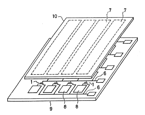
Switch elements 1 such as TFT's scan bus lines 6, and display
electrodes 8 of display elements 5 are formed on a second glass
panel 9, and data bus lines 7 are formed on a first glass panel
10 and it functions as another common display electrode. Between
each display electrode 8 and data bus line 7, liquid crystal med-
ium is held, forming display element 5.
Connections of switch element 1 are shown in Figures 3 and
4, wherein display electrode 8 is connected to one controlled el-
ectrode 3 of switch element 1, control electrode 2 of switch el-
ement 1 is connected to scan bus line 6 (SLn-l), and another con-
trolled electrode 4 of switch element 1 is connected to adjacent
scan bus line 6 (SLn). In operation, the scan bus line SLn having
connection to the controlled electrode 4 of switch element 1 is
scanned just after the scanning of scan bus line SLn-l to which
the control electrode 2 of the switch element 1 is connected.
As seen from Figure 4, scan bus line 6 and data bus line 7
are formed on separate panels 9 and 10 respectively; therefore,
there is no grade-crossing and insulation problem, resulting in an
increase of production yield. And further, bus lines on the se-
cond panel are simplified, and this increases the opening rate.
As for the switch element 1 of the active matrix display de-
vice using liquid crystal medium, TFT is generally used. In this
case, the gate electrode is used as control electrode 2 of switch
element 1, the source electrode is used as controlled electrode 3
and the drain electrode as another controlled electrode 4.
In the above explanation of Figures 3 and 4, controlled ele-
ctrode 4 is connected to a scan bus line 6. However, several mod-
25307-177
ifications are possible in actual fabrication. Scan bus lines and
drain bus lines (conventionally so-called) are separately formed,
wherein the horizontal portions of one group of bus lines can be
formed on another group, forming a double layer structure. If
proper connections are provided between these two layers, it fun-
ctions just as the equivalent circuit shown in Figure 3, and it is
schematically shown in Figure 5.Double layer structure has the mer-
its of obtaining a large opening rate, realizing a lower resistance
of scan bus line and obtaining redundancy thereof.
The drain bus line 14 in Figure 5 can be formed simultaneously
together with display electrode 8, source electrode S, and drain
electrode D with its extension line therefrom, using transparent
conductive material. On the other hand, scan bus line 11 is sub-
sequently formed by metalization process, having an insulating lay-
er therebetween. Connections between the transparent conductive
layer and metalization layer, are achieved by partial removal of
the insulating layer under the scan bus line 11.
Figure 6 shows a plan view of a typical and fundamental con-
figuration of electrode arrangement on the second panel of the
present invention. Display electrode 8 and source electrode S are
formed as a unified plane electrode, and drain electrode D and its
extension line 14a are also formed as one strip-shaped electrode.
All these electrodes are formed using transparent conductive mat-
erial typically known as ITO (Indium Tin Oxide).
The region enclosed by a dot-dash-line indicates that TFT l is
formed in this area. On drain electrode D and source electrode S,
amorphous silicon and insulating layers are deposited and pattern-
ed for this area, and next scan bus line 11 together with gate
16 ~ 38 25307-177
electrode G is formed by metalization process using such as alumi-
num material. Connection between extension line 14a and scan bus
line 11 is made by directly depositing metal layer of scan bus
line 11 on the end portion of extension line 14a.
A cross-sectional view taken along two dot-dash-lines A-X-A'
forming right angle is shown in Figure 7. In the figure, amorphous
silicon layer 16 deposited on drain electrode D and source elec-
trode S, insulating layer 17 made of silicon oxide or silicon ni-
tride, and gate electrode G form stagger-type TFT 1.
The electrode configuration on the first glass panel is com-
paratively simple; therefore, detailed illustration is omitted.
Data bus lines 7 of transparent conductive material are formed on
glass panel 10 and their direction is perpendicular to that of
scan bus lines 6 (11) as shown schematically in Figure 4. Liquid
crystal medium is held between each display electrode 8 and data
bus line 7, forming a display element.
The structure of the present invention includes no grade-cros-
sing of data and scan bus lines on glass panel 9, and no separately
formed earth bus line in the prior art; therefore, large opening
rate can be obtained.
As explained previously, modification of the design especially
with regard to the connection of extension line 14a to scan bus
line is possible.
The first modification is embodied in that the extension lines
14a are formed together with the drain bus line which constitutes a
lower layer of double layer structure, and the structure is shown
in Figures 8 and 9. Figure 8 shows a cross-sectional view taken
along line B-B' of Figure 6; and Figure 9, along line C-C'. Drain
~ 3 8 25307-177
bus line 14 is simultaneously formed and patterned together with
extension line 14a. Amorphous silicon layer 16 and insulating
laye:r 17 are removed except for the area for the TFT 1 region.
Therefore, scan bus line 11 can be formed directly on drain bus
line 14 for a comparatively long distance with regard to each pix-
el. Scan bus line 11 and drain bus line 14 are combined and form
scan bus line 6.
Though the drain bus line 14 is formed separately from scan
bus line in this modification, it is formed within the same pattern
area of scan bus line 11 forming the double layer structure; there-
fore, the same opening rate as that of the device without drain
bus line, can be obtained.
In fabricating the panel structure shown in Figures 6 to 9,
three steps of photolithographic patterning processes are required;
1) patterning transparent conductive layer for forming dis-
play electrode 8, source electrode S , drain electrode D, ex-
tensiOrl line 14a including drain bus line 14 if necessary,
2) patterning amorphous silicon layer 16 and insulating layer
17 for forming active region of TFT 1 and exposing the sur-
face of drain bus line 14, and
3) patterning metal layer for forming gate electrode G and
scan bus line 11.
Step (2) is necessary to form the double layer stucture of
scan bus line, thereby two layers are connected together for each
pixel.
In the second modification of scan bus line design, above
patterning step t2) is omitted. Therefore the fabrication pro-
cesses are very simplified, requiring only two patterning steps.
;38 25307-177
~8
The equivalent circuit for the second modification is shown
in Figure 10, wherein the same reference numerals designate the
same or similar parts. Scan bus line 11 and drain bus line 14 are
not connected together, but they are insulated with each other
within an effective display area on the panel, and two bus lines 11
and 14 are connected on both peripheral regions 25 of the panel.
In this case, a cross-sectional view taken along line B-B' of Fig-
ure 6 is shown in Figure 11.
Scan bus line 11 has distributed capacitances shown as con-
densors 26 in Figure 10. This design is characterized in thatscan bus line 11 can work as well as normal, even when by accident
there is a break in one bus line or a connection fault at one
peripheral terminal, because it is connected through another bus
line via a roundabout circuit.
Drain bus line 14 has a comparatively higher resistance value
than that of scan bus line 11, however, it is coupled capacitively
with the scan bus line. Then the drain current can flow in and
flow out through the capacitance 26 connected to scan bus line 11
parallel with drain bus line 14, therefore, generation of rounded
pulse waveform can be avoided.
Figures 12 and 13 show the structures of scan bus line 11 and
drain bus line 14 at the peripheral region of the panel. Figure
12 shows a plan view, and Figure 13 shows a cross-sectional view
taken along line V-V of Figure 12.
At the peripheral region of the panel, terminals 28 and 27 of
scan bus line 11 and drain bus line 14 are branched off and their
surfaces are exposed. Connector 29 is pressed for engagement (in
the figure, it is shown schematically) and is used for connecting
19 ~ ~ Q ~ 8 25307-177
two bus lines or receiving address pulses.
The structure of this type has a feature in that scan bus line
11 and drain bus line 14 can be connected to the separate power
sources for test purpose.
If the peripheral regions 25 are covered during the depositing
process of amorphous silicon layer 16 and insulating layer 17,
then scan bus line 28 (11) can be directly deposited on drain bus
line 27 (14) in the peripheral regions 25. In this case, connec-
tions between two bus lines are automatically completed.
The third modification fo the panel design is now explained.
When an insulation fault through insulating layer 17 between gate
electrode G and drain electrode D happens, then one scan bus line
11 connected to said gate electrode G and other scan bus line 11
connected to said drain electrode D interact with each other, and
their voltages influence each other very much. This fact causes a
line defect in display. The third modification of design allev-
iates this defect.
Figure 14 shows an equivalent circuit for explaining the
principle of the above modification. The figure is almost the
same as Figures 3 or 5 except that drain electrode D is connected
to scan bus line 6 through resistor 20. This resistor 20 pre-
vents the above interaction between two adjacent scan bus lines.
The line defect is alleviated, the defect being limited to a sin-
gle pixel in which the insulation fault of TFT occurs.
The fabrication method thereof is similar as that applied in
Figures 6 to 9; however, as the transparent conductive material,
Tin Oxide (SnO2) layer having a thickness of 500 A is used for de-
position on the glass panel. It has a sheet resistivity of about
25307-177
50 kilohms per square. The deposited layer of Tin Oxide is then
patterned, resulting in forming display electrode 8, source elec-
trode S, drain electrode D, extension line 14a and drain bus line
14 when the double layer structu~eis adopted.
The extension line 14a has a high resistance of 1 Megohms
when its dimensions are selected as 10 ~m width and 200 ~m length.
On the contrary, scan bus line 11 is formed using a metal layer
such as aluminum; therefore it is easy to obtain a low resistance
such as 10 Kilohms between two end terminals. A resistance ratio
of scan bus line 11 to extension line 14a larger than 1:10 is suf-
ficient for preventing the line defect. Therefore, if the resis-
tance value of scan bus line 11 is assumed to be 10 Kilohms, the
value of 100 Kilohms is enough for the extension line 14a.
When the resistance value of 1 Megohms is adopted for the ex-
tension line 14a, the change of address pulse voltage, applied to
the scan bus line having insulation fault of TFT, can be maintained
within 1~ of normal voltage; therefore, only a single pixel having
the insulation fault in TFT does not work well.
In this embodiment, display electrode 8 is also formed of a
Tin Oxide layer having a high sheet resistivity; however, this does
not become a serious problem, because a resistance value less than
10 Megohms is sufficient to charge up the capacitance between two
display electrodes within the addressing period, when the capaci-
tance is assumed to be 1 pF.
The fourth modification of embodiments is now explained. Fig-
ure 15 shows a plan view of the electrode configuration having two
TFTs 1 and 1' per pixel, and this configuration has the merit of
providing a redundancy for the display device. Its equivalent
21 25307-177
tl~J~ 38
circuit is shown in Figure 16.
Each display electrode 8 is connected to two source electrodes
S and S' of TFTs 1 and 1' respectively which are complementary to
each other. When either of the TFTS has any defect, the other TFT
works effectively. The electrode configuration having a redundan-
cy such as shown in Figure 15 can be realized by a simple bus line
arrangement without a crossover on the substrate. Scan bus line
ll(SLn, SLn+l) is connected to drain electrodes D,D' through lower
bus line 14. Further, neighboring gate electrodes G and G' are
connected to the adjacent scan bus line through extension line 14".
Scan bus line 11 is made of a metal layer and forms a double
layer with the lower bus line 14 of transparent conductive material.
On the other hand, extension line 14" formed between gate electro-
des G, G' and scan bus line 11 is also made of transparent conduc-
tive material such as ITO; therefore it has a resistance R of the
order of 100 Kilohms.
When any one of the TFTs of Figure 16 has a short between gate
electrode and drain electrode, short circuit current flows between
ad~acent scan lines SLn and SLn+l through the resistor R as shown
in Figure 16. As a result the drain voltages of the TFTs con-
nected to the scan line shows a sharp change at the defective TFT
and the display brighness also shows a change, therefore, it is
easy to specify the defective TFT. The defective TFT can be cut-
off by evaporating the connecting portion such as between the
drain electrode and the scan bus line or extension line 14" using
laser radiation through the substrate. In this way, the display
device can be repaired and works normally bv u5in~ the other re-
maining TFT.
$38
22 25307-177
Of course, the electrode configuration of this embodiment can
be modified in such a way that drain electrodes D, D' are connected
to the scan bus line through resistor R and gate electrodes G, G'
are connected to adjacent scan bus line.
The driving method for the above described active matrix dis-
play device is now explained. The equivalent circuit of Figure 3
is used again for explaining the principle.
A TFT (its position in the matrix is represented as TFTmn) is
assumed to be off-state while a voltage between gate electrode 2
and drain/source electrodes 3/4 is equal to or lower than Q volts.
This means that TFT 1 is an n-type enhancement transistor and the
threshold voltage thereof is 0 volts. Due to the requirements of
liquid crystal characteristics, the polarity of the voltage (data
voltage) applied to display element Lmn should be reversed alter-
nately every time when the scan bus line SLn, connected to TFTmn,
is addressed. Address pulses such as Vgl, Vg2 and Vg3 shown on the
left side of Figure 3 are impressed to each scan bus line 6 sequ-
entially synchronized with the horizontal synchronizing signal,
and data pulses such as Vdl and Vd2 shown on the upper side of Fig-
ure 3 are impressed to each data bus line 7 simultaneously for each
horizontal scan period. The polarity of the data voltage is re-
versed after scanning one fr~me. A scan pulse has a stepped wave-
form having Vgoff, Vgc, and Vgon levels.
Figure 18 shows a detailed voltage versus time chart illustra-
ting; (a~ data voltage to DLm, (b) and (c) address pulses to SLn
and SLn+l, (d) display electrode potential Vpmn on TFTmn side, and
(e) voltage across display electrodes of Lmn. Data voltage Va re-
verses its polarity to -Va at t6 as seen in Figure 18(a), where
25307-177
`'J~. ~`38
~t6 - tl) means one frame period; and t4 represents the beginning of
the first pulse of the next frame.
When the address pulse shown in Figure lB (b) is applied, for
example, to scan bus line SLn, then address pulse of Figure 18 (c)
is simultaneously applied to the next scan bus line SLn+l. The
address pulse has three levels as described. When TFTmn is addre-
ssed at time tl, then its gate 2, connected to scan bus line SLn,
is driven to Vgon; data bus line DLm, to Va; and its drain connect-
ed to SLn+l, to Vgc. To maintain the normal operation of display
element according to the present invention, the following voltage
relationship should be satisfied at all times;
Vgc - Vgoff > 2Va,
where threshold voltage Vth is assumed to be 0 volts. The above
condition means that regardless of the polarity of the charged vol-
tag~ between display electrodes and the polarity of the data vol-
tage, TFTmn is maintained at off-state for the whole non-addressed
period, and therefore the charged voltage between display electrod-
es is maintained.
For example, if data voltage Va and -Va are selected as +5
volts and -5 volts respectiv~ly, Vgc - Vgoff should be larger than
10 volts. If Vgc is chosen as 0 volts, then Vgoff should be lower
than -10 volts such as -12 volts.
When threshold voltage Vth has a finite value, the relation-
ship is modified as follows;
Vgc - Vgoff > 2Va - Vth.
When TFTmn of Figure 3 is addressed at tl, the address pulses
~ 8 25307-177
of Figures 18 (b) and 18 (c) are applied to scan bus lines SLn and
SLn+l respectiv~ly, and the data pulse of Figure 18(a) is applied
to data bus line DLm. Then charging current flows into display el-
ement Lmn and the voltage across display electrodes builds up. The
terminal voltage (shown as Vpmn in Figure 3) shows a steep rise
and a fall approaching 0 volts as shown in 18(d), and the charged
voltage across display electrodes is shown in Figure 18(e).
At time t2, TFTmn is turned off and data voltage is changed
to zero. Voltage at Vpmn jumps to -Va level because of capacitive
coupling between the display electrode and data bus line DLm, and
charged voltage across display electrodes as shown in Figure 18 (e)
is maintained almost constant for the subsequent period. During
the subsequent non-addressed period, data bus line DLm receives
data voltage every time when other scan bus lines are addressed.
Therefore non-addressed display element Lmn also receives the ef-
fects of voltage change of data bus line DLm.
However in Figure 18 (e), the charged voltage is simply shown
as constant, neglecting voltage fluctuation. When the data pulse
is assumed to have the waveform shown in Figure 18(a), wherein the
pulse beginning at t3 shows the final data pulse of the first
frame; and data pulse beginning t4, the first data pulse of the
next frame, then the voltage Vpmn of Figure 18(d) also shows two
change~ corresponding to the above two data pulses beginning at t3
..
and t4. At t3, Vpmn rises to 0 volts, and at t4, it drops to -2Va.
It is seen that, when the polarity of the data pulse changes, the
maximum amplitude of Vpmn reaches to twice the data voltage. In
order to maintain TFTmn at off-state for the Vpmn change, Vgc -
Vgoff > 2Va is a necessary condition as described previously for
~ 25307-177
normal operation of the display device.
At t6, TFTmn is addressed by the second pulses of Figures 18
(b) and 18(c) respectively, and the data pulse of -Va is applied to
data bus line DLm. Then the terminal voltage Vpmn shows a steep
drop momentarily below the -Va level, and approaches the 0 level,(Vgc)
because TFTmn is conductive. The direction of the charging current
is opposite to that occurring at tl. Therefore the charged voltage
between display electrodes is also reversed to the -Va level at t6
as shown in Figure 18(e).
When the data voltage is negative, the gate voltage to make
the TFT on-state can be lower than the voltage for positive data
voltage. Therefore, the waveform of the address pulse can take
different shapes depending on the polarity of the data pulse.
Next, the improved driving method of the display device ac-
cording to the present invention is explained. By the previously
explained method using Figure 18, the polarity of data pulses is
reversed alternately every frame. Charged voltage across display
electrodes of Figure 18(e) is shown as a constant line for most
part of non-addressed period, however, in a practical application,
it is affected by data voltages during non-addressed period.
Generally the active matrix display device can not avoid the
influences of leakage current and capacitance between electrodes.
The voltage across display electrodes fluctuates during non-addres-
sed period and this makes the transparency (in other word, bright-
ness) of pixel thereof fluctuate. Data pulses of the same polarity
for one frame period are more liable to such effects than the method
of reversing the polarity every horizontal scan, This is the al-
ready known method of driving the active matrix display device of
26 ~ 38 25307-177
the prior art.
The display device according to the present invention can also
adopt the above method to maintain more correct display brightness,
wherein the application method of data pulses is changed in such
a way that the polarity of data voltage is reversed alternately
every horizontal scan and the polarity to each pixel is further re-
versed every frame.
Even when the above method is applied, there remains fluctu-
ation of the voltage across display electrodes. This is shown in
Figure 17 which corresponds to Figure l~(e). Figure 17 shows the
voltage fluctuates between the solid line and the dashed line.
The electrode structure of the present invention is more sus-
ceptible to data voltage change than those of the prior art, be-
cause display element is connected to scan bus lines through two
capacitances in parallel, one being gate-to-source capacitance;
and second, source-to-drain capacitance.
To avoid the above fluctuation of the display brightness and
keep it at correct values, an improved driving method will be dis-
closed hereinafter.
Figure 19 shows waveforms of; (a) alternate data pulse Vd, and
(b) voltage change (Vb) across display electrodes for the specific
pixel addressed. At first, the pixel is addressed and driven to Vh
or level [l]tfor example, white level), and then for all subsequ-
ent non-addressed period, the pixel receives effects of alternate
voltage change of
~ 3 8 25307-177
-Vh and Vh, both representing level [1]. Fig. 20 shows the
similar waveforms Vd and Vb as Fig. 19 except that data
pulse Vd changes from Vh to -Vl and then to Vl alternately
or all [0] level (black) for the subsequent non-addressed
period.
The voltage Vb receives the effects of data pulses Vd
and it changes its waveform as shown Figs. l9tb), and Fig.
20(b). When r is assumed as an influence factor of pulse
voltage Vd to voltage Vb, it is less than 1, and then
amplitude of Vb shows a fluctuation having an amplitude of
rVh in Fig. l9(b) or rVl in Fig. 20(b).
The brightness of liquid crystal display depends on
the effective voltage (Vb rms) applied across the liquid
crystal display element.
For the case of Fig. l9(b), effective voltage Vb rms
is given by the following equation;
I SlV(t) ] 2dt
Vb rmg = \/ ~S
.
~ ~ 2 ntOVh + 2 ntO (Vh - 2rVh) 2
= ~ Vh2 (2 - 4r + 4r2)
= Vh~ i - 2r + 2r2 , __---(1)
where n denotes number of scan lines; and to~ time of
one horizontal scan.
And for the case of Fig. 20(b), the effective voltage
~ 3 8 25307-177
Vb' rms is given by the following equation;
Vb' rms =
i
¦ toVh2 + ~2(n-l)tO (Vh - rVh + rVl) 2 + ~2ntO(vh - rVh - Vl) 2
V ntO
- ~ ~2[Vh(l - r) + rVl] 2 + ~Vh(l - r) - rVl~ 2
= Vh~ (l-r) 2 ~ (Vh/Vl)2r2 ~ 2)
The difference a v rms between Vb rms and Vb' rms is
given as follows;
r2Vh (1 - Vl2/Vh
V rms -
2 rl - 2r + 2r 2
= r *(Vh - Vl)(Vh + V1)-----(3)
2Vh~ 1 - 2r + 2r2
In order to obtain equal brightness for both cases of
Figs. 19 and 20, the difference ~ V rms of equation (3) is
to be minimized. The driving method therefor is disclosed
hereinafter.
Fig. 21 shows the same equivalent circuit as Fig. 3,
and waveforms of address pulses on the left side and data
pulses on the upper side, waveforms being different from
those shown in Fig. 3. Each time when scan bus line 6 of
the odd number is addressed, data voltage of positive
polarity is applied, and each time when scan bus line of
the even numbers is addressed, data voltage of negative
polarity is applied. Waveforms of data voltage are shown
29 25307-177
~ 3 ~
for both display levels ll] and [0] in accordance with its
polarity.
With regard to address pulse during TFTll is
addressed, pulse voltage Vgon of waveform Vgl is impressed
to scan bus line 61 and voltage of drain electrode 4 of
TFTll connected to scan bus line 62 is maintained at
voltaqe Vgc of waveform Vg2.
Vgc levels of address pulse is different depending on
the polarity of data pulses. According to the driving
method of the present invention, the absolute value of Vgc
is determined as the values of between the saturation
voltage and threshold voltages of liquid crystal display
element.
Transmi3sivity characteristic versus applied voltage
for liquid crystal is shown in Fig. 22. Vt denotes the
threshold voltage; and Vs, the saturation voltage of liquid
crystal display element. In other words, it may be
considered that Vs means the applied voltage of display
element for level [l]; and Vt, for level tO].
And next, conditions for minimizing the brightness
fluctuation are explained. Assume that Vgc of pulse Vgl
for positive data in Fig. 21 is selected as (Vs + Vt)/2 and
Vgc of Vg2 is selected as -((Vs I Vt)/2 for negative data
pulse. And amplitudes of data pulses are selected as (Vs -
Vt)/2 and -(Vs - Vt)/2 as shown on the upper side of Fig.
21 depending on display level and the polarity of data
~ 8 25307 177
voltage.
When positive data voltage (Vs - Vt)/2 for level tl]
is applied to display element 51, and drain of TFTll is
held at voltage of -(Vs + Vt)/2, then voltage across
display element becomes Vs. When positive data voltage
-(Vs - Vt)/2 for level [0] is applied, then voltage across
display element becomes Vt.
When negative data voltage -(Vs - Vt)/2 for level 11]
is applied to display element 52, and drain of TFT12 is
held at voltage of (Vs + Vt)/2, then voltage across display
element becomes -Vs. When negative data voltage (Vs -
Vt)/2 for level [0], then voltage across display element
becomes -Vt.
Therefore, for data pulses of level 11] of positive
and negative polarities, display element is driven to
saturation voltages Vs and -Vs respectively; and for data
pulses of level 10], Vt and -Vt.
In this case, the difference of the effective voltages
a V rms of equation ~3) is obtained by substituting (Vs -
Vt)/2 for Vh, and -(Vs - Vt)/2 for Vl. The last term of
equation (3), namely (Vh ~ Vl), becomes zero.
Actual waveform pattern of data pulse is different
from Fig. 20(a), and it shows the waveform pattern of data
pulse which begins at level 11] similarly with regard to
the first pulse, however, the polarities of the second and
all following pulses for non-addressed period of level 10]
31 25307-177
~ 3
are reversed and their amplitudes are the same as the first
pulse.
The driving method above described has features in
that data voltages have the same amplitude for both levels
~1] and tO] and voltage fluctuation across the display
elements is made smaller.
Fig. 23 shows voltage versus time chart for the
embodiment of the above driving method, wherein (a) shows
data pulses for data bus line DLm; tb) and (c), address
pulses for scan bus lines SLn and S~n+l; (d), display
electrode voltage on TFTmn side; and (e), voltage across
display electrodes Lmn. Numerals +1 and -1 in Fig. 23(a)
denotes level [1] data for positive and negative polarities
respectively. Numerals +0.5 and -0.5 denotes intermediate
level between level [1] and [0~ for positive and negative
polarities respectively. And numerals +0 and -0 denotes
level [0] data for positive and negative polarities
respectively.
The amplitudes of data pulses for levels [1] and [0]
are selected as (Vs -Vt)/2 or -(Vs - Vt)/2 depending on the
polarity as explained in Fig. 21. With regard to the
address pulse shown in Fig. 23~b) applied to scan bus line
SLn, the first pulse Vgl corresponds to positive data pulse
and the second pulse Vgl' corresponds to negative data
pulse after one frame period.
When TFTmn is addressed by the first pulse of Vgl, its
32 ~; ~ 25307 177
drain connected to SLn+l is driven to Vgc having an
amplitude of -(Vs + Vt)/2 as shown in Fig. 23tc). Display
element is charged with the voltage Vs, and is maintained
for subsequent one frame period. It is shown in Fig.
23(e), and it shows potential of the display electrode on
TFT side is negative.
And next when scan bus line SLn+l is addressed,
negative data pulse -~Vs - Vt)/2 of level [1] is applied,
and the drain of TFTmn+l is driven to (Vs + Vt)/2, then
display element is charged with the voltage -Vs.
For displaying brightness of middle level between 11]
and 10] levels, data voltage i8 selected as the middle
value between (Vs -Vt)/2 and -(Vs - Vt)/2, namely, O volts.
The embodiment of Fig. 24 shows a block diagram of the
driving method according to the above embodiment. Scan bus
lines 112 of active matrix display device 111 of the
present invention are addressed by scan bus drivers 115a
and 115b, and data pulses are applied to data bus lines 113
by data bus drivers 114a and 114b. Each scan bus driver
115 comprises shift register 116 and buffer amplifier 117,
and is operatively connected to switching circuit 118.
Display data corresponding to single horizontal scan
line are stored in data bus drivers 114a and 114b, and
outputted to data bus lines 113 synchronized with the
address pulse outputted sequentially to scan bus line 112
from scan bus drivers 115a and 115b. Switching circuits
33 ~ L~ 8 25307-177
118a and 118b are connected to power sources Vl, V2 and V3.
And Vgoff is separately supplied to scan bus drivers.
Vgon, which makes the active element (TFT, not shown in
Fig. 24) conductive, is supplied from Vl. Vgc having a
voltage of (Vs + Vt)/2 is supplied from V2, and Vgc having
a voltage of -(Vs + Vt)/2 is supplied from V3. These
voltages are selectively switched in switching circuits
118a and 118b and outputted selectively to the scan bus
line 112 through buffer amplifiers 117a and 117b. The
voltage sources for Vgoff are separately provided to each
scan bus driver 115, and maintain the voltage of scan bus
lines at Vgoff for non-addressed period.
Fig. 25 shows a waveform versus time chart for the
embodiment of Fig. 24. In the figure, (a) shows horizontal
clock signal; (b), first shift clock signal SCRl; (c),
second shift clock signal SCR2; (d), shift data SD; and (e)
and (f), address pulses from scan bus drivers 115a and 115b
respectively.
Clock signal (a) has period H which corresponds to one
horizontal scan period. The first and second shift clock
signals SCRl and SCR2 have a phase difference of ~/2 with
each other, and shift data SD has one frame period F.
On time t0, the first scan bus line 112 is driven by
Vl having voltage of Vgon by scan bus driver 115a connected
to switching circuit 118a, and at the same time, the next
scan bus line is driven by V3 having voltage of -(Vs I
34 ~ 3 8 25307-177
Vt)~2 by scan bus diver 115b connected to switching circuit
118b. This is shown in the region between t0 and tl of
Figs. 25(e) and 25(f~. Data voltages of positive polarity
corresponding to the first scan bus line are also supplied
to data bus lines 113 during this period.
On time tl, the first scan bus line is driven to Vgoff
by scan bus driver 115a, and the second scan bus line is
driven to Vgon by scan bus driver 115b, and the third scan
bus line is driven to (Vs + Vt)/2 (waveform is not shown in
the figure) by scan bus driver 115a which is connected to
V2 through switching circuit 118a. During the period
between tl and t2 of Fig. 25, data pulses of negative
polarity corresponding to the second scan bus line is
supplied to data bus lines 113.
In the above explanation, horizontal scan progresses
from top to bottom sides. This can be reversed by applying
address pulses from bottom to top sides and by changing the
connections of gate electrode and drain electrode of TFTs,
for example, by connecting gate electrode 2 of TFTll to
scan bus line 62 and drain electrode 4 of TFTll to scan bus
line 61 in Fig. 21.