Note: Descriptions are shown in the official language in which they were submitted.
:1~2~
D/863 2 5
ELECTROPHOTOGRAPHIC IMAGING MEMBER
BACKGROUND OF THE INVENTION
This invention relates in general to electrophotography and
more specifically, to an electrophotographic imaging member and process
for using the imaging member.
In the art of electrophotography an electrophotographic plate
comprising a photoconductive insulating layer on a conductive layer is
imaged by first uniformly electrostatically charging surface of the
photoconductive insulatin~ layer. The plate is then exposed to a pattern of
activating e~ectromagnetic radiation such as light, which seiectively
dissipates the charge in the illuminated areas of the photoconductive
insulating layer while leaving behind an electrostatic latent imaye in the
non-illuminated areas. This electrostatic latent image may then be
developed to form a visible irnage by depositing finely divided
electroscopic toner particles on the surface of the photoconductive
insulating layer. The resulting visible toner image can be transferred to a
suitable receiving member such as paper. This imaging process may be
repeated manytimeswith reusable photocondu*ive insulating layers.
As more advanced, higher speed electrophotographic copiers,
duplicators and printers were developed, degradation of image quality
was encountered during extended cycling. Moreover, complex, highly
sophisticated, duplicating and printing systems operating at very high
speeds have placed stringent requirements including narrow operating
Iimits on photoreceptors. For example, the ground plane of many modern
photo~onductive irnaging members must be highly flexible, adhere weli to
flexibie supporting substrates, and exhibit predictable electrica!
characteristics within narrow operating limits to provide excellent toner
images over many thousands of cycles~
One type of ground plane which is gaining increasing popularity
for belt type photoreceptors is vacuum deposited aluminum coated with
two electrically operative layers, including a charge generating layer and a
charge transport layer. However, aluminurn films are relatively soft and
,.~ 1
~21L31~
exhibit poor scratch resistance during photoreceptor fabrication
processing. In addition, vacuum deposited aluminum exhibits poor optical
transmission stability after extended cycling in xerographic imaging
systems. This poor optical transmission stability is the result of oxidation of
the aluminum ground plane as electric current is passed across the junction
between the metal and photoreceptor. The optical transmission
degradation is continuous and, for systems utilizing erase lamps on the
nonimaging side of the photoconductive web, has necessitated erase
in tensity ad justment every 20,000 copies over the life of the
photoreceptor.
Further, the electrical cyclic stability of an aluminum ground
plane in multilayer structured photoreceptors has been found to be
unstable when cycled thousands of times. The oxides of aluminum which
naturally form on the aluminum rnetal employed as an electrical blocking
layer prevent cnarge injection during charging of the photoconductive
device. If the resistivity of this blocking layer becomes too great, a residual
r potential will build across the layer as the device is cycled. Since the
thickness of the oxide layer on an aluminum ground plane is notstabie, the
electrical performance characteristics of a composite photoreceptor
undergoes changes during electrophotographic cycling. Also, the storage
life of many composite pho-toreceptors utilizing an aluminum grouncl
plane can be as brief as one day at high temperatures and humidity due to
accelerated oxidation of the metal. The accelerated oxidation of the metal
ground plane increases optical transmission, causes copy quali~y non-
uniformity and can ultirnately result in loss of electrical grounding
capability.
After long-term use in an electrophotographic copying
machine, multilayered photoreceptors utilizing the aluminum ground
plane have been observecJ to exhibit a dramatic dark development
potential change between the first cycle and second cycle of the machine
due to cyclic instabiiity, referred to as "cycle 1 to 2 dark developrnent
potential variation". The magnitude of this effect is dependent upon cyclic
age and relatively humidity but may be as large as 350 volts after 50,000
.. . .
- .: , . :: . . ;
~., ' ' ~ : . : .: .
; ~ ,. ., , ; ,
' , ' :: . .. ' , : ' . ,. . : :'
: ' ,',' .: ',:,; ' - . `
~32~31~
electrical cycies. This effect is related to interaction of the ground plane
and photoconductive materials. Another serious effect of the aluminum
ground plane is the loss of image potential with cycling at low relative
humidity. This cycle down voltage is most severe at relative humidities
below about 10 percent. Wi~h continued cycling, the image potential
decreases to a degree where the photoreceptor cannot provide a
satisfactory image in the low humidity atmosphere.
In Japanese Patent Publication J5 6024-356 to Fuji Photo Film
KK, published March 7, 1981, an electrophotographic photoreceptor is
described comprising a conductive support, an inorganic arnorphous silicon
photosensitive layer which produces a charge carrier by photo-irradiation,
and a charge blocking layer between the conductive support and the
inorganic amorphous silicon photosensitive layer, the charge blocking
layer forming a barrier against electric charge carriers. The charge
blocking layer comprises an insulating or serniconductive material such as
SiO2, Al2O3, ZrO2, TiO2 or an organic polyrner such as polycarbonate,
polyvinylbutyral, etc. These charge blocking layer materials are intended
to block electrons into the inorganic amorphous silicon photosensitive
layer. Although not disclosed in this Japanese Patent Publication, it should
be noted that charge blocking layer materials suitable for blocking
electrons into an inorcganic amorphous siiicon photosensitive layer may not
necessarily be suitable for blocking holes into an organic hole generator
layer. To be operable, these blocking layers must not block holes from the
positively charged inorganic amorphous silicon photosensitive layer to the
conductive support. For example, an Al2O3 film having a thickness of
several hundred angstroms utilized as a blocking layer caused dark
deuelopment potential cycie down, with accompanying dark decay, of a
negati\lely charged multilayer structured photoreceptor comprising
concluc~ive ground plane, blocking layer, charge generating layer and a
hole transport layer.
in some multilayered photoreceptors, the ground plane is
titanium coated on a polyester film. The titanium coating is sputtered on
the polyester film in a layer about 175 angstromsthick. The titanium layer
-3-
., ~ . ..
- , . . . .,
- - ~ 1. ~ . , ;
. : : `
l 3213~
acts as a conductive path for electrons during the exposure step in the
photoconductive process and overcomes many of the probiems presented
by aluminum ground planes. Photoreceptors containing titanium ground
planes are described, for example, in U.S. Patent 4,588,667 to Jones et al.
Although excellent toner images may be obtained with multilayered
photoreceptors having a titaniurn ground plane, it has been found that
charge deficient spots form in photoreceptors containing titanium ground
planes, particulariy ùnder the high electrical fields employed in high speed
electrophotographic copiers, duplicators and printers. MoreoYer, the
growth rate in number and size of newly created charge deficient spots
and grow~h rate in size of preexisting charge deficient spots for
photoreceptors cont3ining titanium yround planes are unpredictable from
one batch to the next under what appear to be controlled, substantially
identical fabrication conditions. Charge deficient spots are srnall
unexposed areas on a photoreceptor that fail to retain an electrostatic
charge. These charge deficient spots become visible to the naked eye af~er
development with toner material. On copies prepared by depositing black
tc ner material on white paper, the spots may be white or black depending
upon whether a positive or reversal image development process is
employed. In positive image development, charge deficient spots appear
as whi~e spots in the solid image areas of the final xerographic print. In
other words, the image areas on the photoreceptor corresponding to the
white spot fails to attrac~ toner particles in positive right reading image
development. In reversal image development, black spots appear in
background areas of the final xerographic copy. Thus, for black spots to
form, the char~e deficient spots residing in background areas on the
photoreceptor attract toner particles during reversal image development.
The white spoSs and black spol:s always appear in the same location of the
final electrophotographic copies during cycling of the photoreceptor. The
white spots and black spots do not exhibit any single characteristic shape,
are small in size, and are visible to the naked eye. Generally, these visibie
spots taused by charge deficient spots have an average size of less than
.~
-4-
~,
.... . . .
, ~,: ,,, ,-. . . .
- .; , - : :: . ~ ; .; :: .
:
132~3~ ~
about 200 micrometers. These spots grow in size and total number during
xerographic cycling and become more objectionable with cycling. Thus, for
example tiny spots that are barely visible to the naked eye can grow to a
size of about 150 micrometers. Other spots may be as large as 150
micrometers with fresh photoreceptors. Visual examination of the areas
on the surface of the photoreceptor which correspond to the location of
white spots and black spots reveals no differences in appearance from
other acceptable areas of the photoreceptor. There is no known test to
detect a charge deficient spot other than by forming a ~oner image to
detect the defect.
PRIOR ART STATEMENT
lJ.S. Patent 4,461,819 to Nakagawa et al, issued July 24, 1984 -
Various electrophotographic imaging members are disclosed including one
cornprising, for example, a substrate, a ground plane layer comprising Al,
Ag, Pb, Zn, ~li, Au, Cr, Mo, Ir, Nb, Ta, V, Ti, Pt and the like, and an
amorphous silicon charge generating layer and a charge transport layer. A
barrier layer is preferred to prevent injection of carriers from the substrate
where the charge generating binder layer or the charge transport layer has
a free surface that is charged. Representative barrier layers are MgF2,
Al2O3, SiO, SiO2 and the like insulating inorganic compounds,
polyethylene, polycarbonates, polyurethanes, poly-para-xylylene and the
like insulating compounds, and Au, Ir, Pt, Rh, Pd, Mo and the like metals
This electrophotographic imaging member is charged with a positive
char~e in most ~f the working examples. However, a negative charge is
applied in Examples 8, 9, 14, 17, 18, 19, and 20.
Japanese Patent Publication J5 6024-356 to Fuji Photo Film KK,
published Mar~h 7, 1981 - An electrophotographic photoreceptor is
disclosed comprising a conductive support, an inorganic amorphous silicon
photosensitive layer which procluces a charge carrier by photo-irradiation,
and a charge blocking layer between the conductive support and the
inorganic amorphous silicon photosensitive layer, the charge blocking
layer forming a barrier against electric charge carriers. The charge
blocking layer comprises an insulating or semiconductive material such as
- 5
- - ' - :` -- " ~ , i; . ,: ,
, - ~ ,, :,, : , ;. . ..
.- ,,; ; ~ -
- ~ ~ . . .
`~ 13213~ ~L
SiO2, Al2O3, ZrO2, TiO2 or an organic polymer such as polycarbonate,
poiyvinylbutyral, etc. These charge blocking layer materials are intended
to block electrons into the inorganic amorphous silicon photosensitive
layer.
U.S. Patent 4,588,657 to R. N. Jones et al, issued May 13, 1986 -
An electrophotographic imaging member is disclosed comprising a
substratet a ground plane layer comprising a titanium metal layer
contiguous to the substrate, a charge blocking layer contiguous to the
titanium layer, a charge generating binder layer and a charge transport
layer.
U S Patent 4,439,507 to F. `~. Pan et al, issued March 27, 1984 -
An electrophotographic imaging member is disclosed comprising a
substrate, a conductive layer, a photogenerating layer cornprising certain
resinous material, and a charge transport layer comprising a resinous
binder anci an electrically active diamine material. The conductive layer
includes, for example, aluminum, nickel, brass, gold, titanium, stainless
steel, chromium, graphite and the like. In an alternative embodiment, a
dielectric layer may optionally be positioned between the
photogenerating layer and the aluminum layer. The dielectric layer may
include, for example, Al2O3, silicon oxides, silicon nitrides, titanates and
the like.
lJ.S. Patent 4,582,772 to L. A. Teuscher et al, issuecl April 15, 1986
- An electrophotographic imaging member is disclosed comprising a
substrate, a transmissive semi-conductive layer selected from the group
consisting of indium-tin oxide, cadmium tin oxide, ~in oxide, titanium
oxides, titanium nitrides, titanium silicides, and mixtures thereof, a
photogenerating layer and a charge transport layer, comprising, for
example, an eiectrically active diamine material.
U.S. Patent 4,464,450 to L. A. Teuscher et al, issued August 7,
1984- Ar, electrophoto~raphic imaging member is disclosed comprising a
metal oxide layer, a siloxane film, a photogenerating layer and a charye
transport iayer, comprisincJ, for example, an electrically active diamine
material.
-6
- " ,,
-. - . : .. ~ . : -. .
-. ; . ., ; ,,. . . ; .
; ' : ~ ', , ' ' ; ~ ' ' :: ' '!;, ~,
~32:13~4
U. S. Patent 4,587,189 to Ah-Mee Hor et al, issued
May 6, 1986 - An electrophotographic imaging member is
disclosed comprising a semiconductive or conductive layer,
a photogenerating layer comprising a perylene pigment, and
an aryl amine hole transport layer.
Japanese Patent Publication 59-212844 to Kiyousera
K.K., published December 1, 1983 - An electrophotographic
sensitive body is disclosed comprising an aluminum
substrate and an amorphous silicon layer having reduced
amounts of Fe and/or Mn "To eliminate white spots lack of
density and to enhance potential acceptance...".
Many metals or other materials which are highly
oxidatively stable, form a low energy injection barrier to
the photoconductive material when utilized as a ground
plane in a photoconductive device. A hole blocking layer
will not form on these oxidatively stable layers thus
rendering these devices non-functional as photoconductive
devices. Other metals exhibit other deficiencies of one
kind or another. Prior claims to good blocking layers
refer to the average performance and do not take into
account the fact that there localized areas of charge
injection may be present. Thus, there is a continuing need
for photoreceptors having ground planes that provide
improved resistance to the formation and growth of charge
deficient spots.
SUMMARY OF THE INVENTION
It is, therefore, an object of an aspect of the
present invention to provide an improved photoresponsive
member which overcomes the above-noted disadvantages.
It is an object of an aspect of the present
invention to provide an improved electrophotographic member
having a ground plane which exhibits greater resistance to
the formation of charge deficient spots during cycle.
~32131~ -
It is an object of an aspect of the present
invention to provide a photoconductive imaging member which
exhibits improved resistance to the growth in size of
charge deficient spots during cycliny.
It is an object of an aspect of the present
invention to provide an electrophotographic imaging
member which stabilizes or reduces during
. -7a-
.-
;''" ~'
~ : ;:: .: :: : : :: : ~: : :
: . : . . . i:: :::; : ;
: :: . :~: , . . ,: .
132~3~ `
cycling the size and number of any charge deficient spotsthat may be present prior to cycling.
It is an object of an aspect of the present invention to
provide an electrophotographic imaging member which
maintains optical transmission with cycling.
The ~oregoing objects and others are accomplished
in accordance with this inventi.on by providing an electro-
photographic imaging member having an imaging surface
adapted to accept a negative electrical charge, the
electrophotographic imaging member comprising a metal
ground plane layer comprising zirconium, a hole blocking
layer, a charge generation layer comprising photoconductive
particles dispersed in a film forming resin binder, and a
hole transport layer, the hole transport layer being
substantially non-absorbing in the spectral region at which
the charge generation layer generates and injects photo-
generated holes but being capable of supporting the
injection of photogenerated holes from the charge
generation layer and transporting the holes through the
. charge transport layer.
; Other aspects of this invention are as follows:
--8--
. . .
~32~3~ ~
A flexible electrophotographic imaging member having an
imaging surface adapted to accept a negative electrical charge, said
comprising a substrate, a metal base layer, a thin overcoating metal layer
comprising zirconium contiguous to said me~al base layer, a hole blocking
layer comprising a siloxane contiguous to said thin overcoating metal
layer, said siloxane comprising a reaction product of a hydrolyzed silane
having the structural formula
.,
HO
/R2
HO ~Si - R 1 - N
\R3
HO
wherein Rl i5 an alkylidene group containing 1 to 20 carbon atoms and R2
and R3 are independently selected from the group consisting of H, a lower
alkyl group containing 1 to 3 carbon atoms, a phenyl group, a
poly(ethylene)amino group and an ethylene diarnine group, a a charge
generation layer comprising photoconductive particles dispersed in a film
forming resin binder, and a hole transport layer comprising a resin binder
and a diamine compound.
-8a -
.. - . : , ~ . ~ ; ................. ... :, .. :. ~ .
. . , . . - -- : -: .: ,:. - .. ~ :: .
~321~
An electrophotographic imaging member comprising a
substrate, a metal base layer, a zirconium metal layer, a blocking layer
comprising a siloxane contiguous to said zirconium metal layer, said metal
base layer comprising a metal which oxidizes more slowly than zirconium
during passage of an electric current, said siloxane comprising a reac~ion
product of a hydrolyzed silane having the general formula
HO
HO \ Si - R~ N /R2
\
HO / ~R3
wherein Rl is an a!kylidene group containing 1 to 20 carbon atoms and R2
and R3 are independently selected from the group consisting of H, a lower
alkyl group containing 1 to 3 carbon atoms, a phenyl group, a
poly(ethylene)amino group and an ethylene diamine group, an adhesive
layer comprising a film forming polymer, a charge generation layer
comprising photoconductive par~icles dispersed in a film forming binder,
and a hole transport layer comprising a solid solution of a polycarbonate
resin material and a diarnine compound, said diamine compound having
the general formula:
~ -
,, , . ... , .,.. ~, . . .
~2~3~ ~
N ~N~
X X
wherein X is selected from the group consisting of an alkyl group having
from 1 to about 4 carbon atoms and chlorine.
A photoconcluctive irnaging member of this invention may be
prepared by providing a substrate in a vacuum, sputteriny a layer of
zirconium metal on the substrate in the absence of oxygen to deposit a
ontinuous zirconium metal ground plane layer, exposing the zirconium
metal ground plane layer to ambient conditions, applying a hole blocking
layer on the 7irconium metal layer, ~pplying a charge generation binder
layer on the blocking layer and applying a hole transfer layer on the charge
generation layer. An adhesive layer may optionally be applied between
the hQle biocking layer and charge generation layer. The zirconium layer
may be formed by any suitable coating technique, such as a varuum
clepositing technique. Typical vacuum depositing techniques include
sputtering, magnetron sputtering, RF sputtering, and the like. Magnetron
sputtering of zirconium ontQ a metallized substrate can be effected by a
conventional type sputterin~ module under vacuum conditions in an inert
atrnosphere such as argon, neon, or nitrogen using a high purity zirconium
target. The vacuum conditions are not particularly critical. In general, a
--~c--
, ~,
: . . ~ . - . . . - . ~, . , , , ~ :,
,. - ~ - .. ; .. - ,. .~:
132~4
continuous zirconium film can be attained on a suitable substrate, e.g. a
polyester web substrate such as Myla;~vailable from E.l. du Pont de
Nemours & Co. with magnetron sputtering. It should be understood that
vacuum deposition conditions may all be varied in order to obtain the
desired zirconium thickness. Typical RF sputtering systems such as a
modified Materials Research Corporation Model 8620 Sputtering Module
on a Welch 3102 Turbomolecular Pump is described in
U. S. Pat. No. 3,926,762. This patent also describes
sputtering a thin layer o~ trigonal
selenium onto a substrate which may consist of titanium. Instead of
spu~tering a thin layer of trigonal selenium onto the titanium substrate,
one may sputter a thin layer of zirconium onto the titanium substrate.
Another technique for depositing zirconium by sputtering involves the use
of planar magnetron cathodes in a vacuum chamber. A zirconiurn metal
target plate may be placed on a planar magnetron cathode and the
substrate to be coated can be transported over the zir~onium target plate.
The eathode and target plate are preferably horizontally positioned
perpendicular to the path of substrate travel to ensure that the deposition
of target material across the wid~h c~f the substrate is of uniform thickness.
If desired, a plurality of targets ancl planar magnetron cathodes may be
ernployed to increase throughput, coverage or vary layer composition.
Gen~rally, the vacuum chamber is sealed and the ambient atmosphere is
evacuated to about 5 x 10⁻⁶ mm Hg. This s~ep is immediately followed by
flushing the entire chamber wi~h argon at a partial pressure of about 1 x
10-3 mm Hg to remove most residual wall gas impurities. An atmosphere of
argon at about 1 x 104 mm Hg is introduced into the vacuum chamber in
the r~gion of sputtering. Ele~rical power is then applied to the planar
magnetron and translation of the subs~rate alt approximately 3 to about 8
meters per minute i5 commenced.
if desired, an alloy of zirconium wi~h a sui~able metal such as
niobium, tantalum, vanadium and hafnium, titanium, nickel, stainless
steel, chromium, tun~sten, molybdenum, and the like, and mixtures
thereof may be substituted for the zirconium target to deposit a layer
.
- . .....
" .
~ 3213~ ~
comprising a mixture of the evaporated metals. The target may be made
of a pressed mixture of the metal powders where alloy combina~ions may
be difficult to achieve. The selected combinations of metal powders are
measured, weighed, and thoroughly mixed and compressed to form a
sputtering target. The conductive layer may, in another embodiment of
this invention, comprise a plurality of metal layers with the outermost
metal layer ~i.e. the layer closes1: to the generator layer) comprising at least50 percent by weight of zirconium. At least 7û percent by weight of
zirconiurn is preferred in the outermost metal layer for even better results.
The multiple layers may, for example, all be vacuum deposited or a thin
layer can be vacuum deposited over a thick layer prepared by a different
techniques such as by casting. Typical metals that may be combined with
zirconium include titanium, niobium, tantalum, vanadiurn, ha~nium, and
the like, and mixtures thereof. Thus, as an iliustration, a zirconium metal
layer may be formed in a separate apparatus than that used for previously
depositing a titanium metal layer or multiple layers can be cleposited in the
same apparatus with suitable partitions between the chamber utilized for
depositing the titanium iayer and the chamber utilized for depositing
zirconium layer. The titanium layer may be deposited immediately prior to
the deposition of the zirconium metal layer. Ground planes comprising
zirconium tend to continuously oxidize during xerographic cycling due to
anodizing caused by the passage of electric currents. Thus, it is preferred
that a metal which oxidizes more slowly than zirconium during passage of
an electric current is emplsyed in the region of the conductive layer most
remote from the photoconductive layer of a metal, particularly where the
ground plane is thin and must remain transparent to electromagnetic
radiation and be electrically conductive throughout extended xerographic
cyciing. Metals and/or alloys which oxidize more slowly than zirconium
during passage of an electric current include, for exarnple, titanium, nickel,
gold, stainless steel, silver, brass, platinum, vanadium, nichrome,
molybdenum, and the like. Generally, for rear erase exposure, a
conductive layer light transparency of at least about 15 percent is
desirable. The conductive layer need not be limited to me~als. Other
-10-
... . . . . .. . . . . .
. , ~ .,
` - ~
~32~3~
,
examples of condZuctive layers may be combinations of materials such as
conductiYe indium tin oxidZe as a transparent layer for light having a
wavelength between about 4000 Angstroms and about 7000 Angstroms or
a conductive carbon black dispersed in a plastic binder as an opaque
conductive layer.
Planar magnetrons are commercially available and are
ntanu~actured by companies such as the Industrial Vacuum Engineering
Company, San Mateo, California, Leybold-Heraeus, Germany and U.S., and
General Engineering, England. Ma~netrons generally are operated at
about 500 volts and 12D amps and cooled with water circulated at a rate
sufficient to limit the water exit temperature to about 43C or less. The use
of magnetron sputtering for depositing a metal layer on a substra~e is
described, for example, in UZ.S. Pat. No. 4,322,276 to Meckel et al .
If desired, the zirconium layer may be formed by other suitable
techniques such as in situ on the outZPr surface of the substrate which may
be a metal layer or layer of any other suitable material. Regardless of the
technique employed to form the zirconium layer, a thin layer of zirconium
oxide forms on the outer surface of the zirconium upon exposure to air.
Thus, when other layers overlying the irconium layer are charac~erized as
"contiguous" layers, it is in~ended that these overiying contiguous layers
may, in fact, contact a thin zirconiwm oxide layer that has formed on the
outer surface of the zirconuium layer. If the zirconium layer is sufficiently
thick to be self supporting, no additional underlying member is neeZded
and the 2irconium layer may function as both a substrate and a conduc~ive
ground plane layer. Generally, a zirconium layer thickness of at least a~oout
100 angstroms is desirable to maintain optimum resistance to charge
deficient spots during xerographic cycling. A typical electrical conductJvity
for ~onductive layers for elec~rophotgraphic imaging members in siow
speed copiers is about 102 to 103 ohrns~square. A thickness of at least about
20 angstroms of zirconium onZ a conductive substra~e is sufficient to
provide resistance to gZrowth of charge deficient SpQts.
.~.
.
ZZ
~32~3~
The substrate may be opaque or substantially transparent and
may comprise numerous suitable materials having the required mechanical
properties. Accordingly, this substrate may comprise a layer of an
electricaily non-conductive or conductive material such as an inorganic or
an organic composition As electrically non-conducting materials there
may be employed various resins known for this purpose including
polyesters, polycarbonates, polyamides, polyurethanes, and the like. The
electrically insulating or conductive substrate may be flexible or rigid and
may have any number of many different configurations such as, for
example, a plate, a cylindrical drum, a scroll, an endless flexible belt, and
the like. Preferably, the substrate is in the form of an endless flexible belt
and comprises a commercially available biaxially oriented polyester known
as Myla~vailable from E. I. du Pont de Nemours & Co. or Melinex
available from ICi.
The thickness of the substrate layer depends on numerous
factors, including economical considerations, and thus this layer for a
flexible belt may be of substantial thickness, for e)(ample, over 200
micrometers, or of minimum thickness less than 50 micrometers, provided
there are no adverse affec~s on the final photoconductive device. If the
photoreceptor is a rigid metal drurn, the subs~rate layer can be 5ûO0
microrneters thick. In one flexible belt ernbodiment, the thickness of ~his
layer ranges from ahotlt 65 micrometers ~o about 150 micrometers, and
preferably from about 75 micrometers to abou~ 125 micrometers for
optimum flexibility and minimum stre~ch when cycled around small
diameter rollers, e.g. 12 millimeter diameter rollers. The surface of the
substrate layer is preferably c!eaned prior to coating to promote greater
adhesion of the deposited coating. Cleaning rnay be effected by exposing
the surface of the substrate layer ~o plasma discharge, ion bambardment
and the like.
The conductive layer may vary in ~hickness over substantially
wide ranges depending on the optical transparency desired for the
electrophotoconducti-/e member. Accordingly, the zirconium metal layer
thickness can generally range in thickness of from at least about 20
12-
``` ~ 3 2 ~
angstrorn units to many centimeters. When a flexible photoresponsive
irnaging device is desired, the thickness may be between about 20
angstrom units to about 750 angstrom units, and rnore preferably from
about 50 Angstrom units to about 2Q0 angstrom units for an optimum
combination of electrical conductivity and light transmission.
After deposition of the zirconium metal layer, a hole blocking
layer is applied thereto. The zirconium layer without the hole blocking
layer results in low charge acceptance and the formation of white or black
spots (depending on whether positive or reversal imaging is employed)
which is different in appearance from the spots encountered with the
combination of a titanium ground plane and a blocking layer. Thus a
blocking layer is necessary in combination with the zirconium layer to
achieve low dark decay, adequate charge acceptance and any significan~
reduction in black or white spots caused by charge deficient spots.
Generally, electron blocking layers for positively charged photoreceptors
allow holes from the imaging surface of the photoreceptor to migrate
toward the conductive layer. Thus, an electron blocking layer is normally
not expected to block holes in positively charged photoreceptors such as
photoreceptors coated with charge generating layer and a hole transport
layer. Any suitable hole blocking layer capable of forming an electronic
barrier to holes between the adjacent photoconductive layer and the
underlying zirconium layer may be utili7ed.The hole blockin~ layer may be
organic or inorganic and rnay be deposited by any suitable technique. For
exampie, if the hole blocking layer is soluble in a solvent, it may be applied
as a solution and the solvent can subsequently be removed by any
conventional method such as by drying. Typical blocking layers include
polyvinylbutyral, organosilanes, epoxy resins, polyesters, polyamides,
polyurethanes, pyroxyline vinylidene chloride resin, silicone resins,
fluorocarbon resins and the like containing an organo metallic salt. Other
blocking layer materials include nitrogen containing siloxanes or nitrogen
containing titanium compounds such as trimethoxysilyl propylene
diamine, hydrolyzed trimethoxysilyl propyl ethylene diamine, N-beta-
(aminoethyl) gamma-amino-propyl trimethoxy silane, isopropyl 4-
.
-~3-
. ,.. ~ . . . , ~ , ".. , .,. ., ,. , ... ~ . , ., .. . -
, . . ... ... . ..
~ . . i ,, - ,,
-. . " ; . ..
. ~ , " . ". ,- . - ..
,~ . i .... :... . .; : : ... ..
.,. , , ,: ..
~ 32131~
aminobenzene sulfonyl, di(dodecylbenzene sulfonyl) titanate, isopropyl
di(4-aminobenzoyl) isostearoyl titanate, isopropyl tri(N-ethylamino-
ethylamino) titanate, isopropyl trianthranil titanate, isopropyl tri(N,N-
dimethyl-ethylamino) titanate, titanium-4-amino benzene sulfonat
oxyacetate, titanium 4-aminobenzoate isostearate oxyacetate,
[H2N(CH2)4lCH3Si(OCH3)2. (gamma-aminobutyl) methyl diethoxysilane,
and [H2N(CH2)3]CH3Si(OCH3)2 (gamma-aminopropyl) methyl
diethoxysilane, as disclosed in U.S. Pat. Nos. 4,291,110, 4,338,387,
4,286,033 and 4,2~1,110. A
preferred blocking layer comprises a reaction product between a
hydrolyzed silane and the zirconium oxide layerwhich inherently forms on
the surface of the zirconium layer when exposed to air after deposition.
This combination reduces spots at time 0 and provides electrical stability at
low RH . The hydrolyzed silane hasthe general formula:
_ . _
H --~ o\
S~l\ X--
--HN
HO n, or
_
,: ~
~1 ."
132:13~
R2 ~3 X
N R7
Rl
I
H ~--O--Si--o --- H
_ ~ Y
or mixtures thereof, wherein Rl is an alkylidene group containing 1 to 20
carbon atoms, R2, R3 ancl R7 are independently selected from the group
consisting of H, a lower alkyl group containing 1 to 3 carbon atoms and a
phenyl group, X is an anion of an acid or acidic sal~, n is 1, 2, 3 or 4, and y is
1, ~, 3 or 4. The imaging member is prepared by depositing on the
zirconium oxide layer of zirconium conductive anode layer a coating of an
aqueous solution of the hydrolyzed silane at a pH between about 4 and
about 10, drying the reaction produc~ layer to form a siloxane film and
applying eiectrically operative layers, such as a photogenerator layer and a
hole transport layer, to the siloxane film.
The hydrslyzed silane may be prepared by hydrolyzing a silane
having the following structural formula:
- . .-. . .. . . . . . .. . . ... . .
~L~21314
R40\ R2
/
RsO --- ~"Si - R j - N~
\
~R3
R60
~.
wherein R1 is an alkylidene group containing 1 to 20 carbon atoms, R2 and
R3 are independently selected from H, a lower alkyl group containing t to
3 carbon atoms, a phenyl group and a poly(ethylene)amino or ethylene
diamine group, and R4, Rs and R6 are independently selected from a lower
alkyl group containing 1 to 4 carbon atorns. Typical hydrolyzable silanes
include 3-aminopropyl ~riethoxy silane, (N,N'-dimethyl 3-amino) propyl
triethoxysilane, N,N-d.irnethylamino phenyl triethoxy silane, N-phenyl
aminopropyl trimethoxy silane, trimethoxy silylpropyldiethylene triamine
and mixturesthereof.
If Rl is extended into a long chain, the compound becomes less
stable. Silanes in which R1 contains about 3 to about 6 carbon atoms are
preferred be~ause the molecule is rnore stable, is more ftexible and is under
less strain. Optimum results are achieved when Rl contains 3 carbo
atoms. Satisfactory results are achieved when R~ and R~ are alkyl groups.
Optimum smooth and uniform films are formed with hydrolyzed silanes in
which R2 and R3 are hydrogen. Satisfactory hydrolysis of the silane may be
effected when R4, Rs and R6 are alkyl groups containing 1 to 4 carbon
atoms. When the alkyl groups exceed 4 carbon atoms, hydrolysis becomes
impractically slow. However, hydrolysis of silanes with alkyl grc~ups
containing 2 carbon atoms are preferred for best results.
-1 6-
- .;
~ 3 ~
During hydrolysis of the amino silanes described above, the
alkoxy groups are replaced with hydroxyl groups. As hydrolysis continues,
the hydrolyzed silane takes on the following intermediate general
structure:
HO
HO7Si - R~ - N~
HO R3
After drying, the siloxane reaction product film formed from the
hydrolyzed silane contains larger molecules in which n is equal to or
greater than 6. The reaction product of the hydrolyzed silane may be
linear, partially crc,sslinked, a dimer, a trimer, and the like.
The hydrolyzed silane solution may be prepared by adding
sufficient water to hydrolyze the alkoxy groups attached to the silicon
atom to form a solution. Insufficient water will normally cause the
hydrolyzed silane to form an undesirable gel. Generallyl dilute solutions
are preferred for achievin~ thin coatings. Satisfactory reaction product
films may be achieved with solutions containing from about 0.1 percent by
weight to about 1.5 percent by weight of the silane based on the total
weight of the solution. A solution containing from about 0.05 percent by
weight to about 0.2 percent by weight silane based on the total weight of
solution are preferred for stable solutions which form uniform reaction
product layers. It is important that the pH of the solution of hydrolyzed
silane be carefully controlled to obtain optimum electrical stability. A
solution pH between about 4 and about 10 is preferred. Thick rea~tion
product layers are difficult to form at solution pH greater than about 10.
Moreover, the reaction product film flexibility is also adversely affected
:
-17-
- ~3213~ ~
when utilizing solutions having a pH greater than about 10. Further,
hydrolyzed silane solutions having a pH greater than about 10 or less than
about 4 tend to severely corrode metallic conductive anode layers such as
those containing aluminum during storage of finished photoreceptor
products. Optimum reacti~n product layers are achieved with hydrolyzed
silane solutions having a pH between about 7 and about 8, because
inhibition of cycling-up and cycling-down characteristics of the resulting
treated photoreceptor are maximized. Some tolerable cyclin~-down has
been observed with hydrolyzed amino silane solutions having a pH less
than about 4.
Control of the pH of the hydrolyzed silane solution may be
effected with any suitable organic or inorganic acid or acidic salt. Typical
organic and inorganic acids and acidic salts include acetic acid, citric acid,
formic acid, hydrogen iodide, phosphoric acid, ammonium chloride,
hydrofluorsilicic acid, Bromocresol Green, Brornophenol Blue, p-toluene
sulfonic acid and the like.
If desired, the aqueous solution of hydroiyzed silane may also
contain additives such as polar solvents other than water to promote
improved wetting of the metal oxicle iayer of metallic conductive anode
layers. Improved wetting ensures greater uniformity of reaction between
the hydrolyzed silane and the metal oxide !ayer. Any suitable polar salvent
additive rnay be employed. Typical polar solvents include rnethanol,
ethanol, isopropanol, ~etrahydrofuran, methylcellosolve, ethylcellosolve,
ethoxyethanol, ethylacetate, ethylformate and mixtures thereof.
Optimum wetting is achieved with ethanol as the polar solvent additive.
Generally, the amount of polar solvent added to the hydrolyzed silane
solution is less than about 95 percent based on the total weight of the
solution.
Any suitable technique may be utilized to apply the hydrolyzed
silane solution to the metal oxide layer of a metallic conductive anode
layer. Typical application techniques include spraying, dip coating, roll
coa~ing, wire wound rod coating, and the like. Although it is preferred
that the aqueous solution of hydrolyzed silane be prepared prior to
. ~ , . . . . .
. .
-... . . . .
-~ 132~31~
application to the metal oxide layer, one may apply the silane directly to
the metal oxide layer and hydrolyze the silane in situ by treating the
deposited silane coating with water vapor to form a hydrolyzed silane
solution on the surface of the metal oxide layer in the pH range described
above. The water vapor may be in the form of steam or hurnid air.
Generally, satisfactory results may be achieved when the reaction product
of the hydrolyzed silane and metal oxicle layer forms a layer having a
thickness between about 20 Angstroms and about 2,00û Angstroms. As
the reaction product layer becomes thinner, cycling instability begins to
increase. As the thickness of the reaction product layer increases, the
reaction product layer becomes more non-conducting and residual charge
tends to increase because of trapping of electrons and thicker reaction
procluct ~ilms tend to become brittle. A bri~tle coating is, of course, not
suitable for flexible photoreceptors, particularly in hi~h speed, high
volurne copiers, duplicators and printers. The thicker coatings may,
however, be ac~eptable in rigid photorecep~ors.
Drying or curing of the hydrolyzed silane upon the metal oxide
layer should be conducted at a temperature greater than about room
temperature to provide a reaction product layer having more uniform
electrical properties, more complete conversion of the hydrolyzed si!ane to
siloxanes and less unreacted silanol. Generally, a reaction temperature
between about 100C and about 150C is preferred for rnaximurn
stabiiization of electrochemical properties. The ternpera~ure selected
depends to some ex~en~ on ~he specific metal oxide layer utilized and is
limited by the temperature sensitivity of the substrate. Reaction product
layers havin~ optimum electrochemical stability are obtained when
reactions are conclucted at temperatures of about 135C. The reaction
temperature may be maintained by any suitable technique such as ovens,
forced air ovens, radiant heat lamps, and the like.
The reaction time depends upon the reaction temperatures
used. Thus less reaction time is requiréd when higher reaction
temperatures are employed. Generally, increasing the reaction time
increases the degree of cross-linking of the hydrolyzed silane. Satisfactory
-19-
.
. . . :
- - \
132~3~
results have been achieved with reaction times betwe~n about 0.5 minute
to about 45 minutes at elevated temperatures. For practical purposes,
sufficient cross-linking is achieved by the time the reaction product layer is
dry provided that the pH of the aqueous solution is maintained between
about 4 and about 10.
The reaction may be conducted under any suitable pressure
including atmospheric pressure or in a vacuum. Less heat energy is required
when the reaction is conduc~ed at sub-atmospheric pressures.
One may readily determine whether sufficient condensation
and cross-linking has occurred to form a siloxane reaction product film
having stable electric chemical properties in a machine environment by
merely washing the siloxane reaction product film with water, toluene,
tetrahydrofuran, methylene chloride or cyclohexanone and examining the
washed siloxane reaction product film to cornpare infrared absorption of
Si-O- wavelength bands between about 1,000 to about 1,200 cm l . If the Si-
O- wavelength bands are visible, the degree of reaction is sufficient, i.e.
sufficien~ condensation and cross-linking has occurred, if peaks in the
bands do not diminish from one infrared absorption test to the next. It is
believed that the partially polymerized reaction product contains siloxane
and silanol moieties in the same rnolecl le. The expression "partia.ly ~-
polymerized" is used because totai polymerization is normally not
achievabie even under the most severe drying or curing conditions. The
hydrolyzed silane appears to react with metal hydroxide molecules in the
pores of the metal oxide layer. This siloxane coating is described in U.S.
Patent 4,464,450 to L. A. Tel~scher .
The blocking layer shc uld be continuous and have a thickness of
less than about 0.5 micrometer because greater thicknesses may lead to
undesirably high residual voltage. A blocking layer of between about
0.005 micrometer and about 0.3 micrometer (50 Angstroms - 30~0
Angstroms) is preferred because charge neutralization after the exposure
step is facilita~ed and op~imum electrical performance is achieved. A
thickness of between about 0.03 micrometer and about 0.06 micrometer is
; '
,
-20-
,: ' .: ~ , ~,~ : ` . -
132~31~
preferred for zirconium oxide layers for optimum elec+rical behavior and
reduced charge deficient spot occurrence and growth. Optimum results
are achieved with a siloxane blocking layer. The blocking layer may be
applied by any suitable conventional technique such as spraying, dip
coating, draw bar coating, gravure coating, silk screening, air knife
coating, reverse roll co~ting, vacuum deposition, chemical treatment and
the like. For ccnvenience in obtaining thin layers, the blocking layers are
preferably applied in the form of a dilute solution, with the solvent being
removed after deposition of the coating by conventional techniques such
as by vacuum, heating and the like. Generally, a weight ratio of blocking
layer material and solvent of between about 0.05:10Q and about 0.5:100 is
satisfactory for spray coating.
In some cases, intermediate layers between the blocking layer
and the adjacent generator layer may be desired to improve adhesion or to
act as an electrical barrier layer. If such layers are utilized, they preferablyhave a dry thickness between about 0.04 micron to about 5 microns.
Typical adhesive layers include film-forming polymers such as polyester,
polyvinylbutyrai, polyvinylpyrolidone, polyurethane, polycarbonates
polymethyl methacrylate, mixtures thereof, and the like.
Any suitable photogenerating layer may be applied to the
blocking layer or intermediate layer if one is employed, which can then be
overcoated with a contiguous hole transport layer as described. Examples
of photogenerating layers include inorganic photoconductive particles
such as amorphous selenium, trigonal selenium, and seleniurn alloys
selected from the group consisting of setenium-tellurium, selenium-
tellurium-arsenic, selenium arsenide and mixtures thereof, and organic
photoconductive particles including various phthalocyanine pigment such
as the X-form of metal free phthalocyanine described in U.S. Pat. No.
3,357,989, metal phthalocyanines such as vanadyl phthalocyanine and
copper phthalocyanine, quinacridones available from DuPont under the
tradename Monastral Red, Monastral violet and Monastral Red Y, Vat
orange 1 and Vat orange 3 trade names for dibromo ant anthrone
pigments, benzimidazole perylene, substituted 2,4-diamino-triazines
, , : :
: ,: . . 1: . ,~ :.
, ''' ' ' ~'' ' ~' ' ,' `'
'. ,', ', ~ '
1 3 2 ~
disclosed in U S Pat. No. 3,442,781, polynuclear aromatic quinones
available from Allied Chemical Corporation under the tradename Indofast
Double Scarlet, Indofast Viole~ Lake B, Indofast Brilliant Scarlet and
Indofas~)range, and the like dispersed in a film forming polymeric binder.
Selenium, selenium alloy, benzimidazole perylene, and the like and
mixtures thereof may be formed as a continuous, homogeneous
ph~togenerating layer. Benzimidazole perylene compositions are well
known and described, for example in U.S. Patent 4,587,189, Multi-
photogenerating layer compositions may be utilized where a
photoconductive layer enhances or redu~es the properties of the
photogenerating layer. Examples of this type of configuration are
described in U.S. Patent 4,415,639 . Other suitable photogenerating
materials known in the 2rt may also be utilized, if desired. Charge
generating binder layer comprising particles or layers comprising a
photoconductive material such as vanadyl phthalocyanine, metal free
phthalocyanine, benzimidazole perylene, amorphous selenium, trigonal
selenium, selenium alloys such as selenium-tellurium, selenium-tellurium-
arsenic, selenium arsenide, and the !ike and rnixtures thereof are especially
preferred be~ause o f their sensitivity to white light. Vanadyl
phthalocyanine, metal free phthalocyanine and telluriurn alloys are also
preferred because these materials provide the additional benefit of bein~
sensitive to infra-red light.
Numerous inactive resin materials may be employed in the
photogenerating binder layer including those clescribed, for example, in
U.S. Pat. No. 3,121,006~ Typical organic resinous binders include
thern oplastic and thermosetting resins such as polycarbonates, polyesters,
polyarnides, polyurethanes, poiys~yrenes, poiyarylethers, polyarylsulfones,
polybutadienes, polysulfones, polyethersulfones, polyethylenes,
polypropylenes, polyimides, polymethyipentenes, polyphenylene sulfides,
polyvinyl acetate, polysiloxanes, polyacrylates, polyvinyl acetals,
-22-
, ~ , , ~ ., . - , ............... . ...... ... ... .
. , !: . .. : ~: ; : :;, .:: ' .-, ::,,: : :: :: -:~:: . : :
~32~3~
polyamides, polyimides, amino resins, phenylene oxide resins, terephthalic
acid resins, epoxy resins, phenolic resins, polystyrene and acrylonitrile
copolymers, polyvinylchloride, vinylchloride and vinyl acetate copolymers,
acrylate copolymers, alkyd resins, cellulosic film formers, poly(amide-
imide), styrene-butadiene copolymers, vinylidenechloride-vinylchloride
copolymers, vinylacetate-vinylidenechloride copolymers, styrene-alkyd
resins, and the like. These polymers rnay be block, random or alternating
copolymers.
The photogenerating composition or pigment is present in the
resinous binder composition in various amounts, generaliy, however, from
about 5 percent by volume to about 90 percent by volurne of the
photogenerating pigment is dispersed in about 10 percent by vs:lume to
about 95 percent by volume of the resinous binder, and preferably from
about 20 percent by volume to about 3~ percent by volume of the
photogenerating pigment is dispersed in about 70 percent by volume to
about 80 percent by volume of the resinous binder composition. In one
embodiment about 8 percent by volume of the photogenerating pigment
is dispersed in about 92 percent by volume of the resinous binder
composition.
The photogenerating layer containing photoconductive
compositions and/or pigments and the resinous binder material generally
ranges in thickness of frorn about 0.1 micrometer to about 5.0
micrometers, and preferably has a thickness of from about 0.~ micrometer
to about 3 micrometers. The photogeneratinc1 layer thickness is related to
binder content. Thinner layers with higher pigment loadincJs are
preferred. Higher binder content compositions generally require thicker
layers for photogeneration. Thicknesses outside these ranges can be
selected providing the objectives of the present invention are achieved.
The active charge transport layer may comprise any suitable
transparent organic polymer or non-polymeric material capable of
supporting the injection of photo-generated holes and electrons from the
trigonal selenium binder layer and allowing the transport of these holes or
electrons through the vrganic layer to selectively discharge the surface
-23-
- . . .
, . .
. .: .
. ..
. . . - .. ~ .
. . . . . .. .
. ., ,, .
. .
-:
:~32:~3`1 ~
charge. The active charge transport layer not only serves to transport holes
or electrons, but also protects the photoconductive layer from abrasion or
chemical attack and therefor extends the operating life of the
photoreceptor imaging mernber. The charge transport layer should
exhibit negligible, if any, discharge when exposed to a wavelength of light
useful in xerography, e.g. 4000 angstrorns to 8000 angstroms. Therefore,
the charge transport layer is substantially transparent to radi~tion in a
region in which the photoconductor is to be used. Thus, the active charge
transport layer is a substantially non-photoconductive material which
supports the injection of photogenerated holes from the generation layer.
The active transport layer is normally transparent when exposure is
effected through the active layer to ensure that most of the inciclent
radiation is utilized by the underlying charge carrier generator layer ~or
efficient photogeneration. When used with a transparent substrate,
imagewise exposure may be accomplished through the substrate with all
light passinc through the substrate. In this case, the active transport
material need not be transmitting in the wavelength region of use. The
charge transport iayer in conjunction with the géneration layer in the
instant invention is a material which is an insulator to the extent that an
electrostatic charge placed on the transport layer is not conducted in the
absence of illumination.
The active charge transport layer may comprise an activating
compound useful as an additive dispersed in electricaiiy inactive polymeric
materials making ~hese materials electrically active. These compounds may
be added to polyn-eric materials which are incapable of supporting the
injection of photogenerated holes from the generation material and
incapable of allowing the transport of these holes therethrough. This will
convert the electrically inactiYe polymeric material to a material capable of
supporting the injection of photogenerated holes from the generation
material and capable of allowing the transport of these holes through the
active layer in order to discharge the surface charge on the active layer.
An especially preferred transport layer employed in one of the
two electricaliy operative layers in the multilayer photoconductor of this
-24-
~2~31~
invention comprises from about 25 ~o about 75 percent by weight of at
least one charge transporting aromatic amine compound, and about 75 to
about 25 percent by weight of a polymeric film forming resin in which the
aromatic amine is soluble.
The charge transport layer forming mixture preferably
comprises an aromatic amine compound of one or more compounds
having the general formula:
/N ~R3
wherein Rl and R2 are an aromatic group selected frorn the group
consisting of a substituted or unsubstituted phenyl group, naphthyl group,
and polyphenyl group and R3 is selected from the group consisting of a
substituted O! unsubstituted aryl group, alkyl group having from 1 to 18
carbon atoms and cycloaliphatic compounds having from 3 to 18 carbon
atoms. The substituents should be free form electron withdrawing groups
such as N02 groups, CN groups, and the like. Typical aromatic amine
cornpounds that are represented by this structural formula include:
I. Triphenyl amines such as:
-25-
,,, : , . , ., . , , " .,
- ~ .. ... . . ... .. ..
- - . . -: ,. , .. , ,, ,,:
'.; ' , ' , ! ' '
: .' . ,. ,~ " : - ',.- .
~ ~ . ' .' ' . ' '~
:' ~, ' ' " '. :' '
~32~3~
N
Il. Bis and poly triarylamines such as:
...
Clt3
C N~
~ ~ .
H3C
, ~ .
.
. -26-
,
.
,., . . ,.... . .... .. ,.. .,.-. .-. . . .
. ,: ., ~ -,, ,,~ .. . : . :. , :
- ' --`: `- ` ' ',: ' ' ' ' : ;: ~,:, '`' . ` ' ! ~ .` `: `
' ~
, ~ .:: ,.
. ~ .
~2~31~
Bis arylamine ethers such as:
N~O~N~ and
IV. Bis alkyl-arylamines such as:
H3~ CH3
N ~--N
:: :
A preferred aromatic amine cornpound has the general
formula:
-27-
~2~3~
Rl Rl
N R4 N .
R2 R2
wherein R1, and R2 are defined above and R4 is selected from the group
consisting of a substituted or unsubstituted biphenyl group, diphenyl ether
group, alkyl group having from 1 to 18 carbon atoms, and cycloaliphatic
group having from 3 to 12 carbon atoms. The substituents should be free
form electron wi~hdrawing groups such as NO2 groups, CN groups, and the
like.
Examples of charge transporting aroma~ic amines represented
by the structural forrnulae above for charge transport layers capable of
supporting the injection of photogenerated holes o~ a charge generating
layer and transporting the holes through the charge transport layer
include triphenylmethane, bis(4-diethylamine-2-methylphenyl)
phenylmethane; 4'-4"-bis(diethylamino)-2',2"-dimethyltriphenyl-
methane, N,N'-bis(alkylphenyl)-[1,1'-biphenyl]-4,4'-diamine wherein the
alkyl is, for example, methyl, ethyl, propyl, n~butyl, etc., N,N'-diphenyl-
N,N'-bis(chlorophenyl)-[1, 1 '-biphenyl]-4,4'-diamine, N,N'-diphenyl-N,N'-
bis(3"-methylphenyl)-(1,1'-biphenyl)-4,4'-diamine, and the like dispersed
in an inactive resin binder.
Any suitable inactive resin binder soluble in methylene chloride
or other suitable solvent may be ernployed in the process of this invention.
Typical inactive resin binders soluble in methylene chloride include
polycarbonate resin, polyvinylcarbazole, polyester, polyarylate,
polyacrylate, polyether, polysulfone, and the like. Molecular weights can
vary from about 20,000 to about 1,500,000.
-28-
1321314
-
: .;
The preferred electrically inactive resin materials are
polycarbonate resins have a molecular weight from about 20,000 to about
120,000, more preferably from about 50,000 to about 100,000. The
materials most preferred as the eiectrically inactive resin rnaterial is
poly(4,4'-clipropylidene-diphenylene carbonate) with a molecular weight
of from about 35,000 to about 40,000, available as LexTMn 145 from General
Electric Company; poly(4,4'-isopropylidene-diphenyiene carbonate~ with a
molecular weight of from about 40,0Q0 to about 45,000, available as Lexan
141 from the General Electric Company; a polycarbonate resin having a
molecular weight of from about 50,000 to about 100,000, avaiiable as
Makrolon from Farbenfabricken Bayer A.(i. and a polycarbonate resin
having a moiecular weight of from about 20,000 to about 50,000 available
as Merlon from Mobay Chemical Company. Methylene chloride solvent is a
desirable component of the charge transport layer coating mixture for ;
adequate dissolving of all the components and for its low boiling point.
Examples of photosensitive members having at least two
electrically operative iayers include the charye generator layer and
diamine containing transport layer members disclosed in U.S. Pat. No.
4,265,990, U.S. Pat. No. 4,233,384, U.S. Pat. No. 4,306,008, U.S. Pat. No.
4,299,897 and U.S. Pat. No. 4,439,507.
`:
An especially preferrecl multilayered photoconductor comprises
a charge generation layer comprising a binder layer of photoconductive
material and a contiguous hole transport layer of a polycarbonate resin
material having a molecular weight of from about 20,000 to about 120,000
having dispersed therein from about 25 to about 75 percent by weight of
one or more compounds having the general formula:
....
~;
. . .
- . ~ , . . .
ll321 ~
X ~/ N~ X
wherein X is selected from the group consisting of an alkyl group, having
from 1 to about 4 carbon atoms and chlorine, the photoconductive layer
exhibiting the ~apability of photogeneration of holes and injection of the
holes and the hole transport layer being substantially non-absorbing in the
spectral region at which the photoconductive layer generates and injects
photogenerated holes but beiny capable of supporting the injection of
photogenerated holes from the photoconductive layer and transporting
the holes through the hole transport layer.
Any suitable and conventional technique may be utilized to mix
and thereafter apply the charge transport layer coating mixture to the
charge generating iayer. Typical application techniques include spraying,
dip coating, roll coating, wire wound rod coating, and the like. Although
it is preferred th~at the acid doped methylene chloride be prepared prior to
application to the charge generating layer, one may instead add the acid
to the aromatic amine, to the resin binder or to any combination of the
transport layer components prior to coating. Drying of the deposited
coating may be effected by any suitable conventional technique such as
oven drying, infra red~ radiation drying, air drying and the like. (;enerally,
the thickness of the transport layer is between about 5 micrometers to
about 100 micrometers,~ but thicknesses outside this range can also be
used.
.
-3û-
, - , , , ~ :. .- . ,.. ;. .. .. - : . .. .. . . ... ~, , ,;. ;
13213~
Generally, the ti-ickness of the hole transport layer is between
abou~ 5 to about 100 micrometers, but thicknesses outside this range can
also be used. The hole transport layer should be an insuiator to the extent
that the electrostatic charge placed on the hole transport layer is not
conducted in the absence of illumination at a rate sufficient tG prevent
formation and retention of an electrostatic latent image thereon. In
general, the ratio of the thickness of the hole transport layer to the charge
generator layer is preferably maintained from about 2:1 to 200:1 and in
some instances as great as 40Q: 1.
If desired, any suitable single photoconductive layer capable of
accepting a negative charge may be substituted for the combination of
two electrically active layer described above. Typical single
photoconductive layers include photoconductive particles such as zinc
oxide, amorphous selenium, cadmium sulphide, vanadyl phthalocyanine,
cadmium telluride, cadmium selenide, solid solutions thereof, and the like
dispersed in an inactive film forming polymeric binder.
Any suitable inactive film forming polymeric binder rnay be
employed in the single photoconductive layer capable of accepting a
negative charge. Typical organic film forming polymeric binders inciude
thermoplastic and thermosetting resins such as polycarbonates, polyesters,
polyamides, polyurethanes, polystyrenes, polyarylethers, polyarylsulfones,
polybutadienes, polysulfones, polyethersulfones, polyethylenes,
polypropylenes, polyimides, polymethylpentenes, polyphenylene sulfides,
polyvinyl acetate, polysiloxanes, polyacrylates, polyvinyl acetals,
polyamides, polyimides, amino resins, phenylene oxide resins, terephthalic
acid resins, epoxy resins, phenolic resins, polystyrene and acrylonitrile
copolymers, polyvinylchloride, vinylchloride and vinyl acetate copolymers,
acrylate copolymers, alkyd resins, cellulosic ~ilm formers, poly(amide-
imide), styrene-butadiene copolymers, vinylidenechloride-vinylchloride
copolymers, vinylacetate-vinylidenechloride copolyrners, styrene-alkyd
resins, and the like. These polymers may be block, random or alternating
copolymers. The photoconductive composition or pigment is present in
the resinous binder composition of the single photoconductive layer in
: - - . ~ . , ~ .
,; , , ,- , ~ ;,
~ . , ~ ,. , ' , ,
~ ~ ,
~ 32131 ~
various amounts, generally, however, from about S percent by volume to
about 90 percent by volume of the photoconductive pigment is dispersed
in about 9S percent by volume to about 10 percent by volume of the
resinous binder, and preferabiy from about 10 percent by volurne to about
30 percent by volume of ~he photoconductive pigment is dispersed in
about 90 percent by volume to about 70 percent by volume o~ the resinous
binder composition. In one embodiment about 25 percent by volume of
the photoconductive pigment is dispersed in about 75 percent by volume
of the resinous binder composition. The single photoconductive layer
capable of accepting a necgative charge generally ranges in thickness of
from about 10 micrometer to about 40 rnicrometers, and preferably has a
thickness of from about 20 micrometer to about 30 micrometers.
Thicknesses outside these ranges can be selected providing the objectives
of the present invention are achieved. Typical single photoconductive
layers are described, for example, in U.S. Pat. No. 3,121,006 .
Other layers such as conventional ground strips comprising, for
example, conductive particles dispersed in a film forming binder may be
applied to one edge of the photoreceptor in contact with the zirconium
layer, blocking layer, adhesive layer or charge generating layer.
Optionally, an overcoat layer may also be utilized to improve
resistance to abrasion. In some cases a back coating may be applied to the
side opposite the photoreceptor to provide flatness and/or abrasion
resistance. These overcoating and backcvating layers may comprise
organic polymers or inorganic polymers tha~ are electrically insulatincg or
slightly semi-conductive.
BRIEF DESCRlPTiON OF THE DRAWINGS
A more complete understanding of the process and device of
the present inventiorl can be obtained by reference to the accompanying
drawings wherein:
FIG. 1 is a schematic illustration of a prior a~ photoreceptor
having a single metal ground plane.
-32-
r~
~32~.3~ ~
FIG. 2 is a schematic illustration of one embodiment of a
photoreceptor of this invention having a plurality of ground planes.
FIG. 3 is a schematic illustration of another embodiment of a
photoreceptor of this invention having a plurality of ground planes.
FIG. 4 graphically compares the light transmission characteristics
of various ground planes during cycling.
FIG. 5 is a plurality of photographs of xerographic copies made
from originals of different densities on xerographic photoreceptors
comprising various ground plane materials.
DETAILED DESCRIPTION OFTHE DRAWINGS
In the drawings, FIGS. 1-3 represent several types of
photoreceptor plates. They are basically similar and contain many layers
that are common to the other photoreceptors.
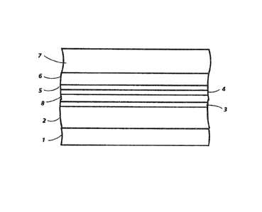
Referring to FIG. 1, a prior art photoreceptor is shown having an
anticurl backing coating 1, a supporting substrate 2, a metal ground plane
3, a blocking layer 4, an adhesive layer 5, a charge generator layer 6, and a
charge transport layer 7.
In Fl(i. 2, a photoreceptor of this invention is illustrated. This
photoreceptor differs from the photoreceptor shown in FIG. 1 in that an
additionai ground plane 8 is employed comprising zirconium.
With referrence to FIG. 3, a photoreceptor of this invention is
shown. This photoreceptor differs from the photoreceptor shown in FIG. 2
in that a thick rigid metal substrate 9 is ernployed rather than the anticurl
backing coating 1, supporting substrate 2 and metal ground plane 3.
In FIG. 4, the light transmission characteristics of various ground
planes during cycling are compared under conditions described in Example
IX. :
Referring to Flti. 5, print tests were performed at the start and
end of cycling tests using normal xerographic development wi~h
photoreceptors having different ground planes. White spots in the solid
image area of copies of originals having a density of 1.1 and 0.5 were
counted and compared. Details of the procedures and results are
described in Exarnple IX.
- . . .~; . ; -
,.,
. :: . ,
.. ... .
~2t3~ ~
The electrophotographic member of the present invention may
be employed in any suitable and conventionai electrophotographic
imaging process which utilizes negative charging prior to imagewise
exposure to activating eiectromagnetic radiation. When the imaging
surface of an electrophotographic member is uniformiy charged with a
negative charge and imagewise e)(posed to activating electromagnetic
radiation, Conventional positive or reversal development techniques may
be employed to form a marking material image on the imaging surface of
the electrophotographic imaging member of this invention. Thus, by
applying a suitable electrical bias and selecting toner having the
appropriate polarity of electrical charge, one may form a toner image in
the negatively charged areas or discharged areas on the imaging surface of
the electrophoto~raphic member of the present invention. More
specifically, for positive development, positively charged toner particles
are attracted to the negatively charged electrostatic areas of the imaging
sur~ace and for reversal development, negatively charged toner particles
are attracted to the discharged areas of the imaging surface.
The electrophotographic mernber of the present invention
exhibits fewer or no charge deficient spots prior to cycling, greater
resistance to the formation of charge deficient spots during cycling, and
improved resistance to the growth in size of charge deficient spots during
cycling. The improvement relating to charge deficient spots provided by
the electrophotographic imaging members of this invention is orders of
magnitude greater that of photoreceptors utilizing a titanium ground
plane. Photoreceptors with aluminum or titaniurn ground planes exhibit a
increase in the number and size of charge deficient spots. Surprisingly, the
electrophotographic member of present invention reduces during cycling
the size and number of any charge c~eficient spots that might be present
prior to cycling. Thus, any charge deficient spots intitially present in
electrophotographic members having a zirconium ground plane appear to
heal and disappear with cycling.
The invention will now be described in detail with respect to the
specific preferred embodiments thereof, it being understood that these
-34-
" r"f, ` ~ ", ", ~ :
1 ~2~3~
examples are intended to be illustrative only and that the invention is not
intended to be limited to the materials, conditions, process parameters and
the like recited herein. All parts and percentages are by weight unless
otherwise indicated.
EXAMPLE I
A polyester film was vacuum coated with a titanium layer
having a thickness of about 200 Angstroms. The exposed surface of the
titanium layer was oxidized by exposure to oxygen in the ambient
atmosphere. A siloxane hole blocking layer was prepared by applying a
Q.22 percent (0.001 mole) solution of 3-aminopropyl triethoxylsilane to the
oxidized surface of the aluminum layer with a gravure applicator. The
deposited coating was dried at 135C in a forced air oven to form a layer
having a thickness of 120 Angstroms. A coating of polyester resin,
Goodyear pF100 (availab!e from the Goodyear Tire an Rubber Co.) was
applied with a gravure applicator to the siloxane coated base. The
polyester resin coating was dried to forrn a film having a thickness of about
0.05 micrometer. A slurry coating solution of 3 percent by weight sodium
doped ~rigonal selenium having a particle size of about 0.05 micrometer to
0.2 micrometer and about 6.8 percent by weight polyvinykarbazole and
2.4 percent by weight N,N'-diphenyl-N,N'-~is(3 methyl phenyl)-~1,1'-
biphenyl]-4,4' diamine in a 1:1 by volume mixture of tetrahydrofuran and
toluene was extrusion coated onto the polyester coating to ~orm a iayer
having a wet thickness of 26 micrometers. The coated mernber was dried
at 135C in a forced air oven to form a layer having a thickness of 2.5
rnicrometers. A charge transport layer was formed on this charge
generator layer by applying a mixture of a 60-40 by weight solution of
Makrolon, a polycarbonate resin having a molecular weight from about
50,000 to about 100,000 available from Farbenfabriken Bayer A. G., and
N,N'-diphenyl-N,N'-bis(3-methylphenyl)-[1 ,1 '-biphenyl]-4,4'-diamine
dissolved in methylene chloride to give a 15 percent by weight solution.
The components were extrusion coated on top of the generator layer and
dried at temperature of about 135C to form a 24 micrometer thick dry
-35-
... ... . - , , , ..................... .~
- , . , . . , :, .
.. . .. . . . .
~ 3 2 ~
layer of hole transporting material. A`grounding strip coating and an anti
curl backing coating were also applied. This photoreceptor was then cut
and welded to form a continuous belt. The photoreceptor was then
mounted in a Xerox 1065 machine for testing. The Xerox 1065 machine is a
xerographic device which drives the photoreceptor belt at a constant
speed of 11.25 inches per second. Charging devices, exposure lights,
magnetic brush developer applicator and erase lights and probes are
mounted around the periphery of the mounted photoreceptor belt. The
photoreceptor was rested in the dark for 60 minutes prior to charging. It
was then negatively corona charged in the dark to a development
potential of 750 v. The photoreceptor was thereafter imagewise exposed
to a test pattern using a light intensity of about S erg/cm2 of light. The
resulting negatively charged electrostatic latent image was developed
with positiveiy charged toner particles applied by a magnetic brush
applicator. After electrostatic transfer of the deposited toner image to a
paper copy sheet, the photoreceptor was discharged (erased) by exposure
to about 500 erglcm2 of light. The toner irnages transferred to the copy
sheets were fused by heated roll fusing. The photoreceptor was then
subjec~ed to the equivalent life of ~00,000 imaging cycles. After initial
copies were made at ambient room conditions (about 35 percent RH and
70F), the machine was then subjected to stress environmental conditions
(10 percent RH, 70F). The machine was cycled without feeding paper. At
the end of the test, the machine was returned to ambient room conditions.
Paper was fed into the machine for imaging. The toner image areas ~f the
imaged copy sheets were examined with a 7x magnifying loupe for white
spots. The area examined was a solid block rectangle (1.4 inches x 2.5
inches) with a 1.1 density \lalue. The number of white spots were circled
and tabulated. The copy sheet from the first imaging cycle had 1 white
spot and the copy sheet from ~he last imaging cycle had 75 white spo~s.
These findings were used to determine growth rate per 100,000 imacging
cycles by dividing (75 white spots - 1 white spot) by 2. Thus, the growth
rate was + 37 white spo~s per 100,000 imaging cycles.
-36-
... . . . . ............ . .. . ... .. .. .. .
- . ~ i . ,. ., . ;: ,, : ., : . ~, .. , . ,:
~3~3~
EXAMPLE ll
The procedures of Example I were repeated with the same
materials except that instead of being vacuum coated with a titanium
layer, the polyester film was coa~ed by sputtering in a vacuum in the
absence of oxygen a zirconium metal layer having a thickness of about 200
Angstroms. Utilizing the testing procedures of Example 1, the
photoreceptor was subjected to 200,000 imaging cycles. The toner image
areas (1.4 inches x 2.5 inches and 1.1 densityj of the imaged copy sheets
were examined for white spots with a 7x magnifying loupe. The copy
sheet from the first irnaging cycle had 25 white spots and the copy sheet
from the last imaging cycle had 8 white spots. This was a growth rate of -9
white spots per 100,000 imaging cycles with the zirconium metal layer of
this invention.
EXAMPLE l l l
The procedures of Example I were repeated with the same
materials except that instead of being vacuum coated only with a single
ti~anium layer, the polyester filrn was coated by sputtering in a vacuum in
the absence of oxygen a titanium metal layer having a thickness of about
65 Angstroms. Without breaking the vacuum, the titaniurn layer was
coated by sputtering, in the absence of oxygen, a zirconium metal layer
having a thickness of about 125 Angstroms. The exposed surface of the
zirconiurn layer was oxidized by exposure ~o oxyyen in the arnbient
atmosphere at elevated temperatures. Utilizing ~he testing procedures
and ~onditions of Exampie 1, the photoreceptor was subjected to 200,000
imaging cycles. The toner image areas of the imaged copy sheets were
examined for white spots with a 7x magnifying loupe. The copy sheet from
the first imaging cycle had 10 white spots and the copy sheet from the last
imaging cycle had 35 white spots. This was a growth rate of + 13 white
spots per 1ûO,000 imaging cycles.
-37-
~32~3~
EXAMPLE IV
The procedures for preparing the photoreceptor belts in
Example I were repeated except that the foliowing rnaterials were
changed. The interface layer was a coating of polyester (duPont 49,000,
available from E.l. duPont de Nemours & Co.) It was applied with a gravure
applicator to the siloxane coated base. The polyester resin coating was
dried to form a film having a thickness of about 0.05 micrometer. The
same charge genera~or layer was applied as in Example 1. The charge
transport layers were the same materials as Example 1. However, the ratios
were 50-50 by weight solution of polycarbonate resin (Makrolon, available
from Farbenfabrikan Bayer A. G.) and N,N'-diphenyl-N,N'-bis(3-methyl
phenyl)-[1,1'-biphenyl]-4,4'-diamine dissolved in methylene chloride. All
other materials and processes were the same as Example 1.
The photoreceptor was welded into a continuous belt and
mounted on a Xerox 1075 duplicator used as a test fixture which drives the
belt at a constant rate of 11.3 inches per second. The Xerox 1075
duplicator contained charging devices, exposure !ights, magnetic brush
developer applicator, and erase lights and probes mounted around the
periphery of the mounted photoreceptor belt.
The photoreceptor was rested in the dark for 15 minutes prior
to charging. It was then negatively corona charged in the dark to a
development poten~ial of -800 volts. The resulting charge photoreceptors
were developed with a reversal toner. Re~ersal toners form deposits in the
discharged areas on the photoreceptor corresponding to the white areas
on the copy paper. To accomplish reversal development, a bias voltage of
600 volts was applied to the developer applicator rolls. With reversal
development, the charge deficient spots print out as black spots in the
charged background areas on the copy paper. In this test sequence, the
photoreceptor was continuously charged and developed with no light
exposure. The test was accomplished at 2i percent RH. The resulting
negatively charged electrostatic latent image was developed with
negatively charged toner particles applied by the magnetic brush
-3~-
~213~4
applicator. After electrostatic transfer of the deposited toner from charge
deficient areas, the photoreceptor was recharged to maintain a
development potential of 800 uniformly over the imaging surface.
In this test, the photoreceptor was cycled continuously for 1
hour. A one square inch area was examined to measure the spot count.
The titanium ground plane photoreceptors had an average of 68 spots per
square inch. After one hour of cycling, the titanium ground plane
photoreceptors had an average of 225 spots per square inch. This was a
growth rate of + 157 white spots per hour of cycling.
EXAMPLE V
The procedures employed in Example IV were repeated except
that instead of being vacuurn coated with a ti~anium layer, the polyester
film was coated by sputtering in a vacuum in the absence of oxygen a
zirconium layer having a thickness of about 200 Angstroms. Utili~ing the
test procedures described in Example IV, the photoreceptor was cycled for
1 hour. The copy sheet was examined for black spo~s in the same manner
as described in Example IV. The copy sheet from the first cycle had 58 spots
per square inch and the copy sheet after 1 hour of cycling had 89 spots ,oer
square inch. This was a growth rate of only + 31 white spots per hour of
cycling with the zirconium layer of this invention.
EXAMPLE Vl
The procedures for preparing the photoreceptor belts in
Exarnple I were repeated except that the following materials were
changecl. The binder generator layer was a slurry coating solution of O.S
percent by weight vanadyl phthalocyanine having a particle size of about
0.2 micrometer and about 4.5 percent by weight polycarbonate resin
having a molecular weight of abou~ 50,0ûO to about 100,000 ~Makrolon,
available frorn Farbenfabriken Bayer, A. G.) dissolved in rnethylene
chloride to give a 5.0 precent by weight solids solution.
The resulting photoreceptor was cut and welded to ~orm a
continuous belt. The photoreceptor was then mounted in a laboratory
-39-
. . ..
- ~ , , ~ . :
~32~3~4
xerographic device which drove the photoreceptor belt at a constant speed
of 6.8 inches per second. Charging devices, exposure lights, magnetic
brush developer applicator, erase lights and probes were mounted around
the periphery of the rnounted photoreceptor belt. The photoreceptor was
rested in the dark for 60 minutes prior to charging. It was then nesatively
corona charged in the dark to a development potential of -750 v. The
photoreceptor was thereafter imagewise exposed to a test pattern using a
light intensity of about 10 erg/cm2 of light. The resulting negatively
charged electrostatic latent image was developed with positively charged
toner particles applied by a magnetic brush applicator. After electrostatic
transfer of ~he deposited toner image to a paper copy sheet, the
photoreceptor was discharged (erased) by exposure to abQut 500 erg/cm2
of light. The toner images transferred to the copy sheets were fused by
heated roll fusing. The machine was then run for 20,000 copies. All of the
copies were prepared at an ambient room conciition of 35 percent RH and
70F. The toner image areas of the imaged copy sheets were examined
with a 7x magnifying loupe for total number of white spots. The area
examined was a solid square block (0.5 inch x 0.5 inch) with a 1.1 density
value. The copy sheet from the first imaging cycle had 176 white spots and
the copy sheet from the last irnaging cycle had 212 white spots. The
growth rate per 100,000 imaging cycles for this 0.25 square inch solid area
block was determined by rnultiplying (212 white spots - 176 white spots) by
5. Thus, the growth rate was + 160 whitespots per 100,000~imaging cycles.
E)(AMPLE Vll
The procedures of Example Vl were repeated with the same
materials except that instead of being vacuum coated with a titanium
layer, the polyester film was coated by sputtering in a vacuum in the
absence of oxygen a zirconium metal layer having a thickness of about 200
Angstroms. Utilizing the testing procedures of Example Vl, the
photoreceptor was subjected to 20,000 imaging cycles. The toner image
areas (0.5 inch x 0.5 inch and 1.1 density) of the imaged copy sheets were
examined for white spots w;th a 7x magnifying loupe. The copy sheet from
-40-
13~1314
the first imaging cycle had 10 white spots and the copy sheet from the last
imaging cycle had 5 white spots. This was a growth rate of -25 white spots
per 100,000 imaging cycles with the zirconium metal layer of this
invention .
EXAMPLE Vlll
The procedures employed in Example IV were repeated except
that instead of being vacuum coated with a titanium layer, the polyester
film was coated by sputtering in a vacuum in the absence of oxygen a
zirconium layer having a thickness of about 200 Angstroms. The silane
blocking lay~er was omitted. All the remaining photoreceptor layers were
coated as in Example IV. Utilizing the test procedures described in Example
IV, the photoreceptor was cycled for 1 hour. The copy sheet was examined
for b!ack spots in the same manner as described in Example IV. The copy
sheet from the first cycle had 3,629 spots per square inch and the copy
sheet after 1 hour of cycling had 2,925 spots per square inch. This test
shows that a zirconlum ground plane without the silane blocking layer is a
poor, non-uniform blocking layer having many localized areas of charge
injection. The spot count is two orders of magnitude higher without a
blocking layer.
Exarnple IX
Sandwich struc~ures having nominal 20 percent light
transmission were prepared using pure Titanium, 30/70 volume ratio
Zirconiumlritanium, SU/S0 volume ratio Zirconium/Titanium, 70/30 volume
ratio Zirconium/Titanium, and pure Zirconium. The rnetals were applied to
a transparent substrate with separate rnagnetron sputtering stations with
the titanium deposited first and the zirconium deposited on top. Metal
thicknesses were adjusted to obtain the 20% optical transmission with the
Titanium to Zirconium ratios described above. Photoreceptors were made
from these ~five combinations of substrates and ground planes by
depositing coatings of a siloxane blocking layer, a polyester adhesive layer
(PE-100, available from Goodyear Tire and Rubber Co.), a charge
-41 -
- : , ; ,
.. .. .
,:- ~ ; :: - ~ "- ~
- . : . : : .
~32~3~
generating layer of tri~onal selenium particles dispersed in a bindert and a
polycarbonate resin and N,N'-diphenyl-N,N'-bis(3-methylphenyl)-[1,1'-
biphenyl]-4,4'-diamine transport layer as described in Example 1. Substrate
oxidation rates were deterrnined by placing circular dot shaped graphite
paint conductive electrodes having a one square centimeter contact area
on top of a portion of the photoreceptor. A constant current of one
microamp was passed through these electrodes on the photoreceptor
using a Trek 610a COR-A-TROL device. After a given number of cycles, one
dot shaped electrode was removed. After another 9,000 cycles, another
electrode was removed and so on for the cycie periods shown in the table
below. The active organic layers of the photoreceptor under the dot
shaped electrodes were removed by washing with methylene chloride and
the transmission of the substrate under each dot shaped electrode was
measured. A graph of transmission versus integrated current (charge) was
then prepared to determine the change in substrate properties as a
function of xerographic cycles. The conversion of charge to xerographic
cycles was accomplished by dividing the total amount of charge passed
through the sample by the amount of charge required for one xerographic
cycle. For a photoreceptor with capàcitance C per square centimenter
charged to an initial potential V the charge per square centimeter Q is
determined by Q=CV. In the test samples, the charge per square
centimeter for one cycle was developed from a capacitance of 100
picofarads per square centimeter and an initial potential of 1,000 volts.
The total amount of charge passed through the sample was divided by the
amount of charge required for one xerographic cycle to determine an
equivalent photoreceptor cycle. The results of the constant current cycling
simulation are presented in the following Table and in Fig. 4.
-42 -
- . , . . - . . ., ;:, . . ~ ., ~ . .:
. ; ;,
. . , ,, ~ .: . ~ ~ :
~32:L31~
TRANSMISSION vs CYCLING OF GROUND PLANES
Cycle100%ZR30Ti/70ZR50ZR/50Ti 100%Ti 70Ti/30ZR
.
0 23 7 21.7 18.7 22.6 21.7
9000 24.0 21.9 19.4 23.0 22.3
18000 24.8 23.5 19.6 23.4 22.9
27Q00 25.6 24.3 20.6 24.3
36000 26.8 ~5.9 ;~ 1.0 24.8 23.
45001) 25.1 24.1
54000 28.7 25.7 21.6 24.1
72000 31.1 28.4 22.2 26.1 23.9
9000(~ 23.0 28.1
108000 35.5 32.4 23.4 26.7
144000 36.7 24.0 26.5
162000
180000 47.2 41.3 2g.9
216000 56.1 47.3 26.4 27.1 27.5
288000 6~.4 ~9.2 30.0
360000 33.3
4320Q0 69.3 29.1 34.4
468000 38.1
57~)00 37.3
648000 48.6
864000 53.0 30.1 37.3
1296000 57.9
1 512000 58.1
As shown in the Table above and in Fig. 4, pure zirconium layer intitially
exhibits about 24 percent light transmission capability and is entirely
oxidized and more transparent after 280,000 cycles. The device with a pure
titanium layer has changed in transmission characteristics from 20 percent
to 26 percent over the same cycling interval. The multiple metal layer
-43-
.
- . ..
~32~ 4
structures have an intermediate oxidation rate determined by the amount
of titanium present.
Photoreceptors were also made with fresh substrates identical
to the substrates described above in this Example and tested for the
equivalent of 200,000 cycles in a Xerox 1065 copier. Print tests were
performed at the start and end of the test using normal xerographic
development. White spots in a solid image area of a copy of an original
having a density of 1.1 were counted and a density per square inch
determined .
WHITE SPOTS
Spots at Spots at Grovvth Rate Per FIG. 5 Row of -
Sample Start End100,000 Cvcles Photos From Top
Pure Ti 1 75+ 37 1st Row
Pure Zr 25 8 -9
Ti/Zr 30/70 4 1 -2 3rd Row
Ti/Zr 50/5040 5 -1~ 5th Row
Ti/Zr 70/30 5 120~ 58
The pure titanium and the multiple metal layer sandwich structures
containing only a small amount of zirconium showed a significant increase
in Charge Deficient Spots with a minimum increase in optical transmission
while the pure zirconium sarnple showed a reduction in the level of Charge
Deficient Spots with a rapid change in transrnission. The samples with 50
percent and 70 percent Zirconium content showed a decrease in charge
Deficien~ Spot level and reasonable transmission change with cycling. A
cornparison of white spots on copies of an original having a density of 0.5
are illustrated in the photographs located in the second, fourth and sixth
rows of FIG. 5. Thus, for copies of originals having a range of densities such
as photographic originals, many more white spots are encountered with
photoreceptors having a titanium ground plane of 100 percenttitanium.
Althoucgh the invention has been described with reference ~o
specific preferred embodiments, it is not intended ~o be limited thereto,
rather those skilled in the art will recognize that variations and
-44-
-: . .; i . .-
- "
~32~3~
modifications may be made therein which are within the spirit of the
invention and within the scope of the claims.
-45-
: ;. ' ;. , ' ' ' .' ~' ' ~
~ , ' . .. . '. ' ~.
: ' , ' ' ' "'`' ' ' ' ~'" "" ,','"" ' . ~ .