Note: Descriptions are shown in the official language in which they were submitted.
1331163 ~ ~ ~
FIELD OF THE INVENTION
This invention is directed to the field of semiconductor processing, and more
2 particularly, to a novel multiple-processing and contamination-free plasma etching
3 system.
BACKGROUND OF THE INVENTION i
4 Plasma etching devices are commonly employed during one or more Or the
phases of the integrated circuit fabrication process, and are typically available in
6 either a single-wafer or a plural-wafer configuration. The single-wafer
7 configurations, while providing excellent process control, suffer from a restricted -
8 system throughput capability. Efforts to relieve the throughput limitations, such
9 as those that have employed faster but higher-temperature etching processes, have
been generally unsuccessful. For these highe~temperature etching processes,
11 system utility is limited due to the undesirable phenomenon of resist "popping",
12 notwithstanding that various cooling approaches have been used including clamping,
13 cooling of the wafer underside with a helium flow, and the mixing of helium into
14 the plasma. The multiple-wafer configurations, while providing a comparatively
much-greater system throughput, have been generally subject to less-than-
16 desirable process and quality control. Not only are end-point determinations for
17 each of the multiple wafers either not available or not precisely determinable, but
18 also electrode positional accuracy for different electrode gaps and correspondingly
19 different gas chemistries is often difficult to establish and maintain. The single-
- 2-
1331163
wafer and the multiple-wafer configurations are both subject to the further
2 disadvantage that two or more step processes typically expose the wafers to an
3 undesirable environment in the intermediate handling step, which mate~ially
4 increases the possibility of wafer oontamination, and which further restricts the
5 processing throughput.
SUMMARY OF THE INVENTION
6 The present invention contemplates plural single-wafer plasma reactors
7 each operative individually to provide excellent process control of single wafers,
8 collectively operative to provide a system throughput limited only by the number
9 of the plural plasma reactors, and so cooperative with a common wafer transfer
and queuing means as to provide both single-step and multiple-step wafer
11 processing in a manner that neither exposes the wafers to an undesirable
12 atmosphere nor to human handling.
13 In the preferred embodiment, plural plasma reactors and a cassette elevator
14 are symmetrically arrayed about an X, IYr movable wafer arm assembly. The
15 plural reactors, the cassette elevator, and the X, TT movable wafer arm are
16 maintained in a controlled vacuum condition, and the central X, TT movable wafer
17 arm is in radial communication with the peripherally surrounding plasma reactors
18 and cassette elevator via a corresponding one of a plurality of vacuum lock valves.
.
19 The arm of the R, TT movable wafer arm assembly includes an apertured platform
20 for supporting each wafer, and a cooperative bumper for releasably engaging the
21 back and the periphery of the supported wafer without any wafer front surface
:.,: ' , . :' ' .. ~.. " '' ' ' .. ' ' . . . .
1331163
contsct. Plural wafer contsct responsive sensors mounted to the platform are
2 operative to provide a signal indication of whether or not the wafer is in a properly
3 seated condition. Each of the plural plasma reactors includes a stationary bottom
4 electrode and a movable upper electrode that are cooperative to provide a variable
5 wafer-cathode to anode gap therebetween of a selectable dimension. ln one
6 embodiment, a support assembly including a micrometer adjustment stop is
7 provided for selectively positioning the movable electrode, and in another
8 embodiment, a combination micrometer stop and pneumatic actuators are providedg for selectively positioning the movable electrode. A vertically movable pedestal is
10 slidably mounted centrally to the stationary electrode of each of the plural plasma
11 reactors that cooperates with the apertured platform of the R, TT movable wafer
12 arm assembly to load and unload the wafers respectively onto and off of the
13 stationary electrode. A reactant gas injection system, a RF power source, and an
14 end-point determination means are operatively coupled to each of the plural
15 plasma reactors. The plural plasma reactors are operable in either embodiment to
16 run the same or different processes, and are cooperative with the R, TT movaMe
17 wafer arm assembly to provide one ~ of the same single-step processing
18 simultaneously in the plural plasma reactors, different single-step processing
19 simultaneously in the plural plasma reactors, and sequential two or more step20 processing in the plural reactors. Two embodiments of the R, TT movable wafer21 arm assembly are disclosed.
; ' '
1331163 ~ ~
: :, ".
DETAILED DESCRIPTION OF THE DRAWINGS . :
.
These and other features, and advantages, of the present invention will
2 become apparent as the invention becomes better understood by referring to the ~ ~
3 following solely-exemplary and non-limiting detailed description of the preferred ~:
4 embodiments thereof, and to the drawings, wherein~
Figure 1 is a pictorial diagram illustrating the multipl~processing and
6 contamination-free plasma etchingsystem accordingto the present invention; ~ .
7 Figure 2 is a fragmentary plan view, partially broken away, of the multiple-
8 processing and contamination-free plasma etching system according to the present
g invention; i:
Figure 3 illustrates in Figure 3A and in Figure 3B partially schematic side :~
11 and end elevational views respectively illustrating the vacuum loclcs intermediate a .
12 corresponding plasma reactor and the R, Tr movable arm assembly of the multiple-
13 processingand contamination-free plasma etchingsystem according to the present
14 invention;
Figure 4 is a partially pictorial and partially sectional view useful in
16 explaining the operation of the R, lT movable wafer arm assembly of the multiple~
17 processing and contamination-free plasma etching system according to the present
1 8 invention;
19 Figure S is a perspective view of a first embodiment of the R, lT movable
20 wafer arm assembly of the multiple-processing and contamination-free plasma
21 etching system according to the present invention; - ~:
_ 5 _
,
r." .. ~
1331163
Figures 6 and 7 are plan views of the first embodiment of the R, lVr movable
wafer arm assembly illustrating different movement positions of the R, rr
movable wafer arm assembly of the multiple-processing and contamination-free
plasma etching system of the present invention;
Figure 8 is a partially broken-away and fragmentary isometric view
illustrating a portion of the first embodiment of the R, IT movable arm assembly
of the multiple-processing and contamination-free plasma etching system of the
present invention; ~:
Figure 9 is a partially pictorial and partially schematic side view illustrating ~:
a plasma reactor of the multiple-processing and contamination-free pl~sma etching
system according to the present invention;
Figure 10 is diagramatic view illustrating the several reactant injection
systems and controlled vacuum system of the multiple-processing and
contamination-free plasma etching system of the present invention, and appears
with Figure l; ~ :
Figure llA is a perspective view and Figure llB is a sectional vlew of a ~.
second embodiment of the R, Tr movable arm assembly of the multiple-processing
and contamination-free plasma etching system of the present invention; ; ~ ~;
Figure 12 is a perspective view of a portion of the second embodiment of
the R, 1~ movable wafer ~rm assembly of the multiple-processing and
contamination-free plasma etching system according to the present invention; and
Figures 13-18 are SEM micrographs illustrating exemplary microstructures
obtainable by the multiple-processing and contamination free plasma etching
system according to the present invention.
1331163
.
D~TAILED DESCRIPTION OF THE PREFERRED EMBODIMENT
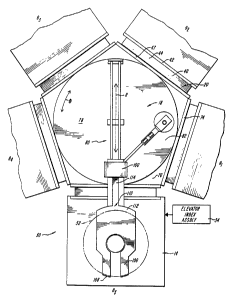
Referring now to Figure 1, generally designsted at 10 is a pictorial diagram
2 illustrating the multiple-processing and contamination-free plasma etching system
3 according to the present invention. The system 10 includes a plurality of single-
4 wafer plasma reactors generally designated 12 to be described and a wafer queuing
station generally designated 14 to be described that are arrayed about a closed
6 locus as illustrated by a dashed line l6. A loadlur~oad module generally
7 designated 18 to be described is dispo6ed concentrically within the plural plasma
8 reactors 12 and the queuing station 14 for singly transferring wafers to be
g processed and after processing between the queuing station 14 and one or more of
the plasma reactors 12. A plurality of vacuum locks generally designated 20 to be
11 described are individually provided at the interfaces of the several plasma
12 reactors la and the load and unload module 18, and between the interface of the
13 queuing station 14 and thé load and unload module 18. A processor 22 is
14 operatively coupled to the plural plasma reactors 12, to the queuing station 14, and
to the load and unload module 18 for activating and de-energizing radio $requency
16 plasma inducing fields in well-known manner, for controlling and processing in
17 well-known manner the signal output of end-point determination means coupled to
18 the several plasma reactors, and for initiating and coordinating wafer transfer
19 between the several reactors snd the queuing station to be described.
A reactant gas injection system 24 to be described is operatively coupled to
21 the plural plasma reactors 12 for controllably injecting preselected reactants and
22 other process gases severally into the plural plasma reactors. A vacuum system 26
-- 7 --
13311~3
is operatively coupled to the reactors 12, to the queuing station 14, and to the load
2 and unload module 18 for maintaining the entire assembly at a controlled vacuum
3 condition during operation. The processor 22 is operatively coupled to the reactant
4 gas injection system and to the vacuum system 26.
S The several reactors 12, the queuing station 14, and the concentric load and
6 unload module 18 conserve space utilization and in such a way as to provide a
7 comparatively-compact plasma etching system. The load and unload module 18 and
8 cooperative ones of the vacuum locks 20 are operable to transfer wafers singly
9 between the queuing station 14 and selected reactors 12 in a single-step processing
mode snd between selected reactors 12 in a two or more step processing mode
11 without any residual or environmentally-induced wafer contamination as well as
12 without intermediate operator handling. Among other additional advantages, the
13 plasma etching system of the present invention is characterized by both an
14 excellent process control and a high processing throughput, the mutual co-
existence of both features having not heretofore been possible in a practicable
16 embodiment.
17 Referrring now to Figure 2, generally designated at 30 is a fragmentary plan
18 view, partially broken-away, illustrating the multiple-processing and19 contamination-free plasma etching system of the present invention. The queuing
station 14 preferably includes a cassette, not shown, having plural vertically-
21 spaced wafers 32 stacked therein. The cassette is preferably mounted for vertical
22 stepping motion by an indexed elevator assembly schematicaUy illustrsted at 34,
23 that is operable under control of the processor a2 (Figure 1) to step the cassette in
24 vertical increments that correspond to the spacing of the verticslly spaced wafers
for addressing the associated cassette slot position. It will be appreciated that in
- 8 -
- 1 3 3 1 1 6 3 : :~
this way individual wafers in the cassette are addressed for removal for processing
2 and for return after processing to their corresponding slot positions. It should be
3 noted that although a cassette and indexed elevator assembly are presently
4 preferred, any other suitable wafer queuing station can be employed as well
without departing from the inventive concept.
6 Referring now to Figures 2, 3A and 3B, the vacuum locks 20 intermediate
7 the gueuing station 14 and the load/unload module 18 and intermediate the plural
8 plasma reactors 12 and the load and unload station 18 each include a housing body
g generally designated 40. The housing 40 includes a plate 42 having opposing top,
bottom, and side walls 44 orthogonal thereto that cooperate to define a generally-
11 rectangular hollow generally designated 46 therewithin as best seen in Figure 3A.
12 A flange 47 is provided peripherally around the walls 44 on the ends thereof remote
13 from the plate 42, and bolts 48 are provided through the ends of the pl~te 42 and of
14 the nange 47 for fastening the housing body 40 at the interfaces between
corresponding ones of the plasma reactors 12 and the load and unload station 18
16 and between the interface between the queuing station 14 and the load and unload
17 station 18. O-rings 50 are provided on the se~ling faces of the plate 42 and
18 flange 47 for providing an air-tight seal. An elongated slot generally designated 54
19 is provided through the plate 47 that is in communicatiop with the generally-
rectangular hollow 46.
21 A chamber door assembly generally designated 56 is cooperative with the
22 slot 54 to provide a valving action. The door assembly 56 includes an elongated,
23 generally-rectangular plate 58 of dimensions selected to be larger than the
24 dimensions of the slot 54. An O-ring sealing member 60 is provided in the sealing
_ g _ -
- .,~,.
- 1331163
face of the plate 58 and surrounding the slot 54. The plate 58 is fastened to an2 arm 62 that is mounted for rotflry motion with a shaft 64' journaled in spaced
3 bearings 66 that are fastened to the plate 42. A chamber door TT-drive actuator,
4 not shown, is fastened to the shaft 64 through an edge of the housing 40 preferably
via a ferrofluidic or other rotary seal as illustrated dashed at 70.
6 The chamber door 56 is pivoted by the chamber door lYr-drive actuator
7 between an open condition, illustrated in dashed outline in Figure 3A, and a closed
8 condition, illustrated in solid outline in Figures 3A and 3B. In Its open condition,
9 the generslly rectangular hollow 46 is in open communication with the elongated
slot 54, so that a wafer arm assembly to be described may readily be moved ir~
11 therethrough between the load and unload station 18 and the several plasma
12 reactors 12 and queuing station 14. In the closed condition of the door
13 assembly 56, the load and unload module is sealed from the plural plasma
14 reactors 12 and from the queuing station 18.
Referring now to Figures 2 and 4, the load and unload module 18 includes a
16 top wall 72, pentagonally-arranged side walls 74, and a pentagonal bottom wall 76
17 deiining an enclosure generally designated 78. A R, TT movable wafer arm
18 assembly generally designated 80 to be described is mounted in the enclosure 78.
19 The assembly 80 includes a turntable 82 mounted for TT-rotation with a shsrt 84
journaled in a bearing assembly generally designated 86 that is fastened in a
21 central aperture provided therefor in the bottom wall 76. A Theta drive motor 88
22 mounted to the bottom wall 76 is operatively coupled to the shaft 84 vis B belt and
23 wheel arrangement generally designated 90. With controlled rotation of the shaft ;~ ~ .
24 of the Theta-motor 889 the shaft 84 and therewith the turntable 82 rotates to any ~
- 10 - ' ~. , ., ~,
. ~
1331I63
selected angular TT orientation for aligning the wafer arm assembly 80 with any
2 one of the plasma reactors 12 or with the queuing station 14 at the corresponding
3 TTl, rr2, rr3, TT4, and 1~5 coordinates.
4 A shaft 92 is concentricslly mounted within the shaft 84 and journaled for
S rotation therein on a bearing and vacuum seal assembly generaUy designated 93.
6 Any suitable rotary vacuum seal, such as a ferrofluidic rotary vacuum seal, may be -~
7 employed. One end of the shaft 92 is connected to a pivot bearing 94 to be
8 described vacuum-mounted through the turntable 82, and the other end of the
9 shaft 92 is operatively coupled to a R-drive motor 96 via a belt and wheel
arrangement generally designated 98. As described more fully below, with the
11 controlled rotation of the shaft of the ~-drive motor 96, the wafer arm of both
12 embodiments of the R, TT movable wafer arm assembly to be described is13 controllably translated in the R-direction for loading and unloading individual
14 wafers into and out of the plural reaction chambers 12 and queuing sta~ion 14
through the associated vacuum lock 20.
16 Referring now to Figures 2, 4, and 5, the wafer arm assembly 80 includes a
17 wafer receiving and releasing paddle assembly generally designated 100. The
18 paddle assembly 100 includes a platform 102 having a central opening generally
19 designated 104 therethrough. The member 102 terminates in lateraUy spaced
fingers 106 having wafer-periphery engaging upstanding flanges 108 integrally
21 formed on the free ends thereof. A releasable abutment generaUy designated 110
22 having a bumper portion 112 and an integral tail portion 114 is mounted for sliding
23 motion to the platform member 102. As best seen in Figure 8, a coil spring 116 is
24 mounted between the relessable abutment 110 and the member 102 which urges the
- 11 - ',:
- 1331163
bumper 112 in the direction of an arrow 118 so as to abut and therewith frictionally
2 engage the periphery of a wafer, not shown, received between the bumper 112 and
3 the flanges 108. The tail 114 includes a downwardly de2ending stop 120 to be
4 described that is slidably received in an elongated aperture provided therefor in the
platform member 102 that is cooperative with an upstanding abutment to be
6 described to release the frictional wafer engagernent as the arm reaches its
7 position of maximum extension. The paddle sssembly lO0 is mounted between
8 plates 124 to a carriage assembly generaUy designated 126 that is slidably mounted
g on linear bearings 128 thst are fastened to end posts 130 upstanding from and
fastened to the rotatable turntable 82.
11 The carriage 126 is controllably moved in either direction along the linear
12 bearings 128 for loading anq unloading wafers individually to and from the several
13 plasma reactors 12 and the queuing station 18. A member 131 is pivotally mounted
14 subjacent the carriage 126, which houses therein a linear bearing, not shown. A
shsft 132 is slidably received through the linear bearing of the pivoting
16 housing 131. One end of the shaft 132 is slidaMy mounted in a sleeve 134 that is
17 mounted for rotary motion to the turntable 82 via a pivot bearing 136, and the
18 other end of the shaft 132 is fastened to a needle bearing assembly 138 that is
19 pivotally fastened to a crank arm 140 mounted for rotation with the shaft 92 of the
R-drive motor 96 (Figure 4) via a mounting coupling 142 fastened to the
21 turntable 82.
22 With controlled rotation of the Theta-drive motor 88, the turntable 82 and
23 therewith the paddle assembly 100 is rotated to that 1~ coordinate that
24 corresponds to any selected one of the angular locations of the plursl plssms
'
- 12 -
~;
- 1331163
reaction chambers designated TTl th~ough 1~ 4 in Pigure 2, and to thst 'IT
2 coordinate that corresponds to the angular location of the wafer queuing station 14
3 designated TT5 in Figure 2. With the controlled rotation of the R-drive motor 96,
4 the crank 140 traces an arcuate path as illustrated by an arrow 144. The arm 132
therewith pivots on the pivot bearing 136 as shown by an arrow 146, and moves the
6 carriage 126 linearly along the bearings 128 in a direction that corresponds to the
7 sense of rotation of the X-drive motor as illustrated by an arrow 148. The arm is . ~ .
.
8 either more or less elongated relative to the coupling 136 as it is pivoted by the . .
g crank 140, and depending on the sense of the rotation, it slides within the
sleeve 134 and within the housing 131 as illustrated by an arrow lSO. When the
11 crank 140 is turned to its maximum clockwise position, the paddle assembly 100
12 moves into its fully retracted position as illustrated generally at 152 in Figure 6. ~ -
13 With counterclockwise motion of the crank arm 140 the paddle moves along the R
14 direction as illustrated generally at 154 in Figure 7. As the paddle assembly 100
nears its fully extended position, close to the maximum allowed counterclockwise16 rotation of the R-drive motor, the stop l20 on the tail portion llO abuts the
17 confronting wall of the upstanding end post 130, such that with continued motion of
18 the paddle along the R direction the bumper 110 draws away from the flanges 108 ~ .
19 and thereby releases the frictional engagement of the wafer periphery. In the
maximum extended position, then, the wafers are free to be loaded or unloaded to21 and from any selected plasma reactor 12 and/or are free for pick up or delivery
22 back into the queuingstation 14. ;
23 Contacts lS6, preferably three in number, are mow~ted to the platform
24 member loa of the paddle assembly 100 as shown in Figure 7. The contacts are
-13- ~ :
.
,' . '-
- 1331163
operative in response to the presence of a supported wafer to provide a three-point
2 signal indicative of whether or not the wafer is properly seated on the wsfer
3 transfer arm. The contacts preferably are formed on a printed circuit board, not
4 shown, mounted to the paddle assembly lOO. A different number thereof, or other
sensing means may be utilized, so long as an accurate indication of intended
6 seating of individual wafers is provided.
7 Referring now to Figure 9, generally designated at 160 is a partially
8 pictorial and partially schematic side view illustrating a plasma reactor of the
g multiple-processing and contamination-free plasma etching system according to
lO the present invention. Each of the plasma reactors 160 includes a top plate 162, a
11 spaced-apart bottom plate 164 and a cylindrical sidewall 166 cooperate to define a
12 plasma chamber generally designated 168. A first electrode generally
13 designated 170 is fastened to the bottom plate 164. A pedestal schemstically
14 illustrated dashed at 172 is slidably mounted centrally in the bottom electrode 170
15 for vertical motion with the shaft of a pnuematic cylinder schematically illustrated
16 in dashed outline 174. As described more fully below, the pedest~l 172 is
17 cooperative with the paddle arm assen~bly to allow for removal and delivery of
18 individual wafers into and out of the plasma chambers. The pedestal pnuematic
19 cylinder 174 is driven by a controlled air supply, not shown, operatively coupled ;-
thereto via an air input port 176 and an air output port 178. As illustrated by
21 dashed outline 180, a source of cooling liquid, not shown, is coupled to internal
22 fluid flow passageways, not shown, provided through the interior of the bottom
23 electrode 170 via input and output ports 182, 184 for removing the heat produced in
24 the bottom electrode during plasma etching. -
- 14--
- ~331163
A top electrode generally designated 186 is fastened to ~ support shaft
2 generally designated 188 that is slidably received through the top plate 162 in a
3 vacuum-tight sealing engagement therewith as by a stainless steel vacuum4 bellows 190 fastened between the top plate 162 and a superadja2ent shaft support
plate 187. The top electrode 186 includes intemal cooling/heating fluid flow
6 passageways schematically illustrated in dashed outline 189 that are coupled ~ria
7 fluid flow conduits 190 disposed in the shaft 188 to a source, not shown, via a liquid
8 input port 194 and an output port 196 provided in the plate assembly 187. A
g pneumatic actuator generally designated 200 having a ram 202 is mounted to the
support plste assembly 187. With the ram 202 in its extended position, not shown,
11 the plate 187 moves upwardly, and therewith the shaft 18B and electrode 186 move
12 upwardly and away from the stationary bottom electrode 170. With the ram
13 lowered as shown, micrometer adjustment posts 204 fastened to the plate14 assembly l87 bear against the top plate l62 and therewith support the top
electrode 186 in an intended spaced-apart relation with the bottom electrode 170.
16 The gap between the electrodes is adjustable by changing the length of the
17 micrometer adjustment posts selectively. In the preferred embodiment, between
18 3/16 inch to 2 inches of gap adjustment is provided.
.: . . :
19 The shaft 188 has a hollow interior generally designated 206, and a laser
window 208 is mounted across the hollow of the shaft 206. The beam of an
21 external laser, not shown, passes through the window and hollow shaft for providing
22 end~point determinations of the plasma etch state. Other en~point determination
23 means, such as a lateral optical detector, may be employed as well without -~
24 departing from the inventive concept. Reactant gas injection ports 210 are
.
--15--
1331163
coupled via intern~l shaft conduits provided therefor, not shown, to a liquid-cooled
2 showerhead gas manifold illustrated in dashed outline 211 in the upper
3 electrode 186. Reactant gas is controllably released therefrom into the plasma
4 reactor, and radio frequency power (e.g. low frequency at typically 5-450
KHz, or microwave typically at 1-4 gHz or high frequency at typically 1-5
6 MHz) i5 applied in the plasm reaction chambers. In an alternative embodi-
7 ment, the spacing between the electrodes can be preselected for each
8 particular plasma process, and additional micrometers, in place of the
g pneumatic actuators 200, can advantageously be employed. ~;
Referring now to Figure 10, generally designated at 212 is a schematic
11 diagram illustrating the presently preferred gas injection and controlled vacuum
12 systems. Preferably, four independently valved sources of gases are respectively ~
13 connected to individual ones of the plasma vessels via corresponding ones of a ~ `-
14 plurality of gas manifolds, two banks of gas sources generally designated 214, 216
and two manifolds 218, 220 being specifically illustrated. A vacuum system 222 is
16 operatively coupled in common to the plural plasma reactor chambers, to the
17 queuing station224, and to the load and unload island226. The vacuum system
18 controls the vacuum condition in the entire system, so that the wafers are free
19 from possible contamination as the vacuum locks are severally opened and closed
during single and multiple phase processing wafer transfer. It should be noted that
21 while four plasma reactors are disclosed, a greater or a lesser number can be
22 employed without departing from the inventive concept.
23 Referring now to Figure 11A, generally designated at 230 is a perspective
24 view of an alternative embodiment of the X, TT wafer arm assembly according to
the present invention. The assembly 230 includes a pully 232 mounted for rotation
26 with the shaft Or the TT drive motor as best seen in Figure 118. The pulley 232
-16-
,. '
- 1331163 ~
includes A grooved rim 234 around which a cable 236 is wrapped. The cable is
2 drawn tangentally to the grooved rib 234 in opposing directions, and respectively
3 wrapped over pulleys 238, 240 and tied to 8 slide 242, as best seen at 244 in
4 Figure 11B. With the angular rotation of the pulley 232, the slide 242 linearly
moves along the the linear bearings 246. A wafer arm generally designated 248 is6 mounted for movement with the slide 242 such that the arm 248 is controllably
7 extended and retracted in dependence on the angular position of the pulley 232. To
8 provide constant-tension in the cable 236, the ends of the cable preferably are
g terminated in the slide 242 agQinst resilient bissing elements generally
. ~ .
designated 250 in Figure 12. The cable 236 as it stretches is pulled in a reverse
11 direction by the resilient couplings 250 for maintaining its intended state.
12 During the plasma chamber load cycles, the Theta-drive motor turns the
13 turntable of the R, TT wafer arm assembly to the TT coordinate of the gueuing
14 station in either embodiment of the R, TT movable wafer arm assembly. The
vacuum lock of the assoeiated interface is released, and the arm is extended under
16 the wafer in the addressed cassette slot position. The arm is then retracted back
17 into the load and unload module, and the vacuum lock is restored. The R, TT water
18 arm assembly is then rotated to the TT coordinate of the selected plasma reactor.
19 The associated chamber door is then rotated to its open condition for providing
20 access to the selected reaction chamber, and the upper electrode is raised. The
21 wafer receiving arm is then extended in the R direction through the associated slot
22 valve opening and into the selected reaction chamber. As it approaches the limit
23 of its maximum radial travel, the depending stop flange on the wafer arm abuts the
24 upstanding end post on the turntable and, with continued radial motion, the bumper
--17--
1331163
withdraws thereby freeing the vrafer from peripheral friction engagement. The
2 cental pedestal of the lower electrode is then controllably rasied by its pneumatic
3 actuator, and therewith the wafer supported on the arm is elevated upwardly off of
4 the wafer support platform. Thereafter, the wafer arm is retracted out of the , ;~
plasma chamber though the open slot valve and back into the load and unload -
6 station. The pedestal is then controllably lowered. The wafer lowers therewith
-:
7 until the pedestal is in its retracted position and the wafer is supported on the
8 surface of the lower electrode. The associated chamber door is then closed, and
9 the upper electrode is lowered to that precise preselected gap that implements the
particular plasma process being run. The intended reactants are then injected
11 through the gas manifold of the upper electrode, and radio frequency power is
12 applied. Whereupon, plasma etching of each single wafer is continued until the
13 laser provides a signal indication that the proper end-point has been acheived.
14 Thereafter, the RF power is turned-off, the vacuum lock is opened, and the above~
described process is repeated, but in reverse order, for removing the wafer out of
16 that plasma chamber and back into the load and unload station. The wafer can
17 then be moved into another plasma reactor for a subsequent proceæ in a two or
18 more step processing mode, or back into the cassette in a one-step processing
19 mode.
The load and unload module, queuing station, and plural reactors are
21 operable in three basic modes, namely, where each reactor is simultaneously
22 performing the same plasma reaction, where each pl~sma reactor is simultaneously
23 performlng two or more different plasma processes, and where the plasma reactors
24 are severally being operated to provide multiple-step processing of single wafers
- 18-
..,,, . , . .. ~, ~, . . . . .
1331163
before their return back to the queuing statior~. In each c~se, the wafers are
2 transferred and processed in 8 controlled vacuum environment such that3 atmospheric exposure and handling induced contamination are wholly eliminated.
4 Figure 13-17 are scannina electron micrographs illustrating exemplary
., ; ,
microstructures capable of being formed in a single-step process, and Figure 18 is a
6 scanning electron micrograph illustrsting an exemplary microstructure capable of
7 being fabricated in a double~tep etch process. Figure 13 shows generally at 260
8 polysilicon with an overlayed photoresist 262 on the surface of the silicon dixoide
g layer 264 of the wafer. For exemplary low-resistivity (12-30 ohms) doped
polysilicon, CCl4 at 20sccn and He at 30 sccm are applied to the plasma reactor at
11 a pressure of 100 mt and fl power of 300 watts. The etch occurs for approximately
12 2 1/2 minutes. As shown in Figure 14 doped polysilicon 265 having a comparatively
13 high resistivity (30-200 ohms per sq.) and having a slopped profile mssk is
14 illustrated. For the illustrated microstructure, SF6 at 50 sccm and freon 115
(C2ClF5) at S0 sccm are controllably injected into a plasma reactor at 150 mt
16 pressure and a 100 watt power. After about 2 1/2 minutes, the illustrated doped
17 polysilicon microstructure is fabricated.
18 Referring now to Fi~Orure lS, generally designated at 266 is a SEM illustrating
19 an exemplary trench etch. The photoresist is removed, and a trench generally
designated 268 is formed in the silicon 272 by injecting BC13 at S sccm and Cl2 at
21 25 sccm into the plasma reactor at a 100 mt chamber pressure and at 750 watts
22 power for about 20 minutes.
23 Referring now to Figure 16, refractory silicide, TaSi/poly, is illustrated
24 generally at 274. The silicon dioxide surfsce 276 is overlayed with a polysilicon
- 19 - : :
:
~ ~. ... .,.; . : . .
;: ~
1331163
layer 278 upon which is overlayed the TaSi/poly 280, over which is the photoresist.
2 The microstructure is fabricated by mjecting CCl4 at 20 sccm and He at 30 sccm
3 into a plasma reactor maintained at a chamber pressure of 80 mt and a radio4 frequency power of 300 watts for about 3 1/2 minutes.
Referring now to Figure 17, generally designated at 282 is another
6 microstructure exemplary of the single-step structures capable of being fabricated
7 by the contamination-free and multiple-processing plasma reactor of the present
O invention. As illustrated, a photoresist 284 is layed over an aluminum and silicon
g layer 286 which is overlayed via a TiW layer ass on the wafer surface. The
illustrated structure was fabricated by injecting BCl3 at 50 sccm with Cl2 at 1511 sccm into the plasma reactor maintained at 12S mt chamber pressure ~nd a 300
12 watt RF power for about a 1/2 to 3 1/2 minutes.
13 Referring now to Figure 18, generally designated at 290 is a silicon
14 dioxide/poly/silicon dioxide/poly sandwich structure illustrating an exemplary two-
step process. A poly layer designated poly 1 and an oxide layer designed oxide are
16 formed after etching with CaF6 at 100 sccm at a 700 mt pressure and a 600 watt
17 radio frequency power in a first chamber. Thereafter, the upper poly 2 layer and
18 the oxide and an overlayed photoresist layer are formed by a separate step
1~ employing CCl4 at 20 sccm and He at 30 sccm in a second reaction chamber
maintained at a 100 militore chamber pressure and a 600 watt radio frequency
2 1 power.
22 Many modifications of the presently disclosed invention will become
23 apparent to those skilled in the art without departing from the scope of the
24 appended claims.
-20-