Note: Descriptions are shown in the official language in which they were submitted.
- 1
1~383~2
TITLE OF THE INVENTION
IMAGE PROCESSING APPARATUS
BACKGROUND OF THE INVENTION
1. Field of the Invention
The present invention relates to an image processing
apparatus and, more particularly, to an image processing
apparatus arranged to detect the outline of input image data
and then to effect color conversion of the detected outline.
2. Description of the Related Art
In recent years, widespread use has been found for
digital color copying machines which are arranged first to
read a color original by utilizing a digital color separation
process, second to apply a desired process to the thus-read
digital image signal, and third to produce a color copy on
the basis of the digital color image signal obtained. In
order to faithfully reproduce the color and sharpness of the
original, this kind of apparatus is designed first to read an
image signal by means of a CCD, second to convert the image
signal into a digital signal by means of an A/D converter,
and third to apply various processes, such as color masking,
under color removal, tone compensation and the like.
~L
-2 - 1338342
Particularly recently, digital color copying machines have
been proposed which are provided with a simple form of a
color-image processing function such as cutting, moving,
synthesizing or the like. In such a situation in which the
degree of fineness of recorded images is improved and the
number of functions incorporated into a copying machine
increases, it has been strongly desired to realize, in
addition to the above-described color-image processing
function, the color conversion function of replacing image
data representing the color of a particular region on an
original with data representing a different color.
However, in a case where such color conversion is
conducted with a proposed method or apparatus, if the color
of a character body on an original is color-converted, the
outline of the character body is also converted into the same
color. Accordingly, if the outline and the character body of
a particular character are to be emphasized independently of
each other, it has been necessary to draw the outline portion
by hand with a color pen or the like. This problem applies
to not only emphasis on characters but emphasis on graphics.
SUMMARY OF THE INVENTION
It is, therefore, an object of the present invention to
provide an image processing apparatus which is capable of
detecting data representing the outline portion of image data
and of independently converting the color of the portion
-
~3 ~ 1~38~2
other than the outline and the color of the outline portion.
It is another object of the present invention to provide
an image processing apparatus which is capable of emphasizing
a portion of an image or of increasing the visual effect of
the image by emphasizing the outline thereof.
It is another object of the present invention to provide
an image processing apparatus which is capable of increasing
the visual effect of an image by shading the image.
It is a further object of the present invention to
provide an image processing apparatus which is capable of
providing, in realtime, an output image in which at least one
portion of an input image and the region which surrounds this
portion are painted in an arbitrary color. It is another
object of the present invention to provide an image
processing apparatus which is capable of forming an outline-
image by extracting only outline portion.
To achieve the above objects, an image processing
apparatus according to the present invention is provided with
means for extracting the outline portion so as to effect
color conversion of the outline portion independently. The
image processing apparatus is also provided with means for
detecting a predetermined color so as to effect color
conversion according to a combination of the portion having
the predetermined color and the outline portion. The
apparatus is also provided with another means for extracting
4 13383~2
an outline portion so as to effect different color conversion
in correspondence with the position of the outline portion.
In addition, the apparatus is arranged to apply color
conversion to a predetermined region near the outline portion
or to apply color conversion to the portion other than the
outline portion.
As described above, in accordance with the present
invention, there are provided various arrangements which can
increase the visual effect of a pattern such as a character
or a graphic image by emphasizing its outline. Further
objects, features and advantages of the present invention
will become apparent from the following detailed description
of embodiments of the present invention with reference to the
accompanying drawings.
BRIEF DESCRIPTION OF THE DRAWINGS
Fig. 1 is a block diagram showing the construction of a
first embodiment of an image processing apparatus according
to the present invention;
Figs. 2A to 2F are vies which serve to illustrate
examples of the results of processes executed by
corresponding embodiments of the image processing apparatus
according to the present invention;
Fig. 3 is a block diagram diagrammatically showing the
construction of the first embodiment of the image processing
apparatus according to the present invention;
~5 ~ 1 3 3 8 3 ~ 2
Fig. 4 is a block diagram diagrammatically showing the
construction of the outline extracting section shown in Fig.
3;
Fig. 5A is a circuit diagram showing the outline
extracting circuit of Fig. 4;
Fig. 5B is a view showing one example of the filter
utilized in the circuit of Fig. 5A;
Fig. 6 is a block diagram showing the color identifying
section used in the first embodiment;
Fig. 7 is a circuit diagram showing the smoothing
section of Fig. 6;
Fig. 8 is a circuit diagram showing the converting-
picture element detecting circuit of Fig. 6;
Fig. 9 is a view which serves to illustrate each mode
for detecting a color;
Fig. lOA is a block diagram showing the construction of
the block processing section of Fig.'6;
Fig. lOB is a view which serves to illustrate the
relationship between an objective picture element and
peripheral picture elements;
Fig. 11 is a block diagram showing the construction of
the color converting circuit used in the embodiment shown in
Fig. 1;
Fig. 12 is a circuit diagram showing an example of a
circuit for generating a select signal to control each
-6 - 13383~2
selector in the color converting circuit of Fig. 11;
Fig. 13 is a schematic diagram showing an example of the
image processing executed in a conventional digital color
copylng machlne;
Fig. 14 is a flow chart showing the operation of CPU in
the first embodiment;
Fig. 15 is a block diagram schematically showing the
construction of a second embodiment of the image processing
apparatus according to the present invention;
Fig. 16 is a timing chart showing the behaviors of
primary signals in the second embodiment;
Fig. 17 is a block diagram schematically showing the
construction of the outline extracting circuit used in the
second embodiment;
Fig. 18 is a block diagram showing the construction of
the front portion of the color identifying section of the
second embodiment;
Fig. 19 is a block diagram showing the construction of
the rear portion of the color identifying section of the
second embodiment;
Fig. 20 is a block diagram showing schematically showing
the construction of the color converting section incorporated
in the second embodiment;
Fig. 21 is a block diagram showing schematically showing
the construction of the color converting section incorporated
13383~2
in a third embodiment;
Fig. 22 is a block diagram which serves to illustrate
the construction of a ratio computing circuit in the color
identifying section of the third embodiment;
Fig. 23 is a block diagram showing a fourth embodiment
of the image processing apparatus according to the present
invention;
Fig. 24 is a flow chart showing the operation of CPU 610
in the fourth embodiment;
Fig. 25 is a block diagram showing a first outline
processing circuit, a second outline processing circuit, and
a non-process circuit in the fourth embodiment;
Figs. 26A, 26B and 26C show examples of a matrix of a
filter;
Fig. 27 is a block diagram showing an outline-color
converting circuit according to the fourth embodiment;
Fig. 28 is a block diagram showing a fifth embodiment of
the image processing apparatus according to the present
invention;
Fig. 29 is a circuit diagram showing an example of the
outline extracting circuit of the fifth embodiment and an
example of the color converting circuit of the same;
Fig. 30 is a circuit diagram showing an example of the
outline extracting circuit according to the fifth embodiment;
Fig. 31 is a block diagram showing a sixth embodiment of
-
1338~2
the image processing apparatus according to the present
inventlon;
Fig. 32 is a block diagram which serves to illustrate a
binary-coding circuit according to the sixth embodiment;
Figs. 33 and 34 are block diagram which serves to
illustrate a block processing circuit according to the sixth
embodiment;
Fig. 35 is a view which serves to illustrate a block
process according to the sixth embodiment;
Figs. 36A and 36B are views showing specific examples of
the results of the processes executed according to the sixth
embodiment;
Fig. 37 is a block diagram of an eighth embodiment of
the image processing apparatus according to the present
invention;
Fig. 38 is a view showing an example of a filter for
extracting an outline in according with the eighth
embodiment;
Figs. 39 and 40 are circuit diagrams showing the outline
extracting circuit of the eighth embodiment;
Figs. 41 and 42 are block diagrams which serve to
illustrate the block process executed in the eighth
embodiment;
Fig. 43 is a block diagram which serves to illustrate a
seventh embodiment of the present invention;
- 9
13383~2
Figs. 44A to 44F are diagrammatic views which serve to
illustrate the operation of the region generating circuit
used in each of the embodiments;
Fig. 45 is a diagrammatic view showing the construction
of a printer for use with each of the embodiments;
Fig. 46 is a graphic representation showing the
relationship between the vertical synchronizing signal of a
red signal and that of a black signal in each of the
embodiments;
Fig. 47A is a block diagram showing an example of a
pulse-width modulating circuit for use in each of the
embodiments; and
Figs. 47B and 47C are timing charts showing signals
which flow in various portions of the pulse-width modulating
circuit.
DESCRIPTION OF THE PREFERRED EMBODIMENTS
Embodiments of the present invention will be described
below in detail with reference to the accompanying drawings.
As shown in Fig. 13, digital color copying machines are
in general arranged to read an image signal from a CCD,
convert the image signal into a digital signal by means of an
A/D converter, and subject the digitized image data to
various processes such as color masking, under color removal
and tone compensation in order to achieve faithful
reproduction of the color and sharpness of an original
-lo- 13383~2
document. In each embodiment which will be described later,
a unique color-conversion function which will be illustrated
below is combined with the above arrangement so that desired
color conversion, particularly outline emphasis, can be
realized.
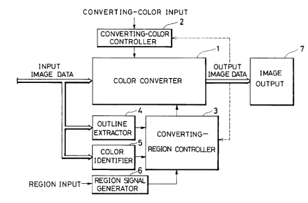
Fig. 1 is a block diagram showing the construction of a
portion for performing the color-conversion function in an
image processing apparatus according to a first embodiment of
the present invention. In the figure, a color converting
section 1 is arranged to convert input image data into output
image data under the control of a converting-color
controlling section 2 or a converting-region controlling
section 3 and then to provide the output image data. This
output image data is recorded by means of an image output
section 7 such as a printer or the like. The input image
data is also input to an outline extracting section 4 for
extracting an outline and a color identifying section for
detecting a predetermined color. The output signals of the
outline extracting section 4 and the color identifying
section 5 are input to the converting-region controlling
section 3 together with the region signal supplied from a
region-signal generating section 6 for designating a
particular region to which color conversion is to be applied.
The converting-region controlling section 3 in turn controls
the color converting section 1 so as to execute various kinds
-11- 1338342
of outline emphasis, which will be described in detail below,
on the basis of the combination of the conditions conveyed by
the above-described designations. The converting-color
controlling section 2 for controlling the converting color
and the converting-region controlling section 3 cooperate to
provide control over the color converting section 1, thereby
enabling an increase in the number of kinds of color
conversion possible.
First of all, the outline emphases which will be
explained below in the description of the preferred
embodiments will be briefly summarized with reference to
Figs 2A to 2F. Fig. 2A shows input image data which
represents, for example, a character "L" in black. Fig. 2B
shows a conventional example of color conversion, in which
case the black character "L" is converted into a red
character "L". Fig. 2C is a view showing an example of color
conversion executed in accordance with any of first to third
embodiments or a portion of a fourth embodiment. The black
character "L" is converted into a pattern consisting of a red
character body and a yellow outline portion.
Fig. 2D is a view showing an example of color conversion
which will be illustrated in one part of the description of
the fourth embodiment; in this example, a red shadow is added
to a color-converted character "L". Fig. 2E is a view
showing an example of color conversion according to sixth and
-12 - 13383~2
seventh embodiments, and in this example, the outline of a
color-converted character "L" is surrounded by a red portion
having a predetermined width. Fig. 2F is a view showing an
example of color conversion according to the seventh
embodiment, and in this example, a color-converted character
"L" consists of a red interior and a red portion having a
predetermined width and extending along the outline thereof
with the color of the outline remaining non-converted.
The color of each of the above examples is only
illustrative and is not of course limitative. As a matter of
course, any of the desired color conversion methods according
to the respective embodiments may be incorporated into the
image processing apparatus of the present invention, or a
combination of a plurality of color conversion methods may be
utilized.
Several embodiments will be explained below in more
detail.
FIRST EMBODIMENT (Independent Color Conversion
of Outline)
Fig. 3 is a block diagram schematically showing the
construction of the first embodiment of the image processing
apparatus.
The illustrated image processing apparatus includes a
CPU 100 for controlling the entire apparatus, a ROM 101 which
stores a control program for the CPU 100 and various types of
-13 - 1338~42
data, and a RAM 102 which is used as a work area for the CPU
100 and which serves to temporarily store image data or
various types of data. The apparatus also includes an I/O
port 103 which connects a system bus 110 with a region
generating circuit 104, a color identifying/converting
circuit 105, and other circuits. A digitizer 106 is used to
designate the position, region, etc. of image data, and is
connected to the bus 110 through a serial interface 107.
Further, the illustrated apparatus includes an outline
generating circuit 104 and an outline extracting section 108
both of which will be described later. Reference numeral
100' represents input image data, and reference numeral 101'
represents output image data.
The CPU 100 supplies the data required for color
identification and color conversion to a plurality of
registers (to be described later) of the circuit 105 through
the I/O port 103 for storage purposes in accordance with the
control program stored in the ROM 101 and shown in the flow
chart of Fig. 15. The region generating circuit 104 creates
a region signal 111 on the basis of the coordinate value
entered from the digitizer 106 and then supplies the region
signal 111 to the color identifying/converting circuit 105.
Fig. 4 is a block diagram schematically showing the
construction of the outline extracting section 108 shown in
Fig. 3.
- -14 - 1338342
As illustrated, the outline extracting section 108
includes an outline extracting circuit 36 for color
separation data R (red data), an outline extracting circuit
37 for color separation data G (green data), an outline
extracting circuit 38 for color separation data B (blue
data), an OR gate 39 for ORing outline information 44, 45 and
46 which correspond to R, G and B, respectively, and timing
adjusting circuits 40, 41, 42 and 43.
In order to synchronize each of the color separation
data R, G and B with any delay occurring in a color detecting
circuit as will be described later, the respective color
separation data are delayed when passed through the timing
adjusting circuits 41, 42 and 43. Since, in this embodiment,
each of the color separation data is delayed by one line, it
is possible to easily realize the timing adjusting circuits
41, 42 and 43 by utilizing, in practice, FIFO memories each
having a memory capacity for one line. The outputs delayed
by one line in the timing adjusting circuits 41, 42 and 43
are input to the respective outline extracting circuits 36,
37 and 38.
The construction of one of the outline extracting
circuits 36 to 38 is shown in Fig. 5A.
In Fig. 5A, FIFO memories 50 and 51 are provided for
delaying input image data by one line, and each of them is
arranged to sequentially receive image data 49 and to return
_ -15 - 13383~2
a write position and a read position to respective initial
positions in response to an HSYNC signal. Of the illustrated
outputs, an output 52 is image data representing an objective
line, an output 53 is image data representing the line
immediately previous to the objective line, and an output 49
is image data representing the line subsequent to the
objective line. Inverter circuits, adders and D-type flip-
flops are denoted by 54, 55 and 56, respectively. A
multiplier 59 multiplies the image data 52 representing the
objective line by four and inputs the result to the
corresponding adder 55. A register 57 stores a threshold
value which serves as a reference value used to identify an
outline, the threshold value being supplied from the CPU 100.
A comparator 58 compares the threshold value stored in the
register 57 with the output value of the adder 55 located at
the last position, thereby outputting the signal (44, 45 or
46) representing a particular region.
A write clock WCK and a read clock RCK of each of the
FIFO memories 50 and 51 are common to the clocks used in the
timing adjusting circuits 41, 42 and 43 and so on. A write
reset signal WRST and a read reset signal RRST are obtained
by inverting the horizontal synchronizing signal HSYNC.
Accordingly, the outputs 52 and 53 constitute image signals
each of which is delayed by one line, as described above.
Fig. 5B is a diagram showing arithmetic operations
-
-16- 1338~42
concerning the filter realized in the circuit of Fig. 5A, and
outline information is extracted by a comparison between the
result of the arithmetic operations and a set threshold
value. In Fig. 5A, reference numeral 61 denotes image data
S obtained by multiplying the image data 52 by the numerical
value "4" shown at (~) in Fig. SB, and reference numeral 62
denotes image data obtained by performing arithmetic
operations using the numerical value shown at (~) + the
numerical value shown at (~3 in Fig. SB. The image data 52
10 represents data obtained by performing arithmetic operations
using the numerical value shown at (~) in Fig. 5B, and an
output 63 represents the result of the arithmetic operations
using the numerical value shown at (~) in Fig. 5B. All the
results are added in the adder 55 located at the last
15 position. In this manner, the arithmetic operations
utilizing the filter shown in Fig. 5B are carried out, and
the result of the multiplication of an objective picture
element by utilizing the filter of Fig. 5B is output to the
comparator 58. The comparator 58 compares the result with
20 the threshold value stored in the register 57 to determine
whether or not the result represents an outline. If the
result represents an outline, the comparator 58 outputs "1".
Each of the flip-flops 56 shown in Fig. 5A delays data
by one picture element to perform timing adjustment, and each
25 of the inverter circuits 54 performs a multiplication of
~ -17 - 13383~2
X (-1) .
Referring back to Fig. 4, the construction of the
outline extracting section 108 will be explained. The
respective outputs 44 to 46 from the outline extracting
circuits 36 to 38 are input to the OR circuit 39. If it is
determined, in the OR circuit 39, that at least one of the R,
G and B signals represents an outline, the output of the OR
circuit 39 goes to "1" whereby it is determined that the
objective picture element is contained in an outline portion.
The timing adjusting circuit 40 has a function similar to
those of the timing adjusting circuits 41 to 43 described
above, and is provided in order to make adjustments
corresponding to any delay occurring in the color detecting
circuit which will be described later. The timing adjusting
circuit 40 is composed of such devices as, for example, D-
type flip-flops, and provides a delay equivalent to
approximately eleven to nineteen clocks.
The color identifying/converting circuit 105 will be
explained below with reference to Figs. 6 to 12.
First, the outline of algorithms for color
identification will be explained. It is known that, if two
representations of a given color are the same (in the case of
a certain hue), the relationship between, for example, the
red (R) signal, the green (G) signal and the blue (B) signal
(hereinafter referred as "R1", "G1" and "B1", respectively)
13383~2
-18 -
will be represented by an equal ratio. Data MC representing
one color (or maximum-value color; hereinafter called "main
color") of certain colors to be color-converted is selected,
and the ratio of the data MC to the r~m~;n;ng two colors is
obtained. For example, if the main color is R, the ratio of
G1 to MC and the ratio of B1 to MC are obtained. From the
input data Ri, Gi and Bi, the following relationships are
obtained:
Ri x (G1/MC) x 1 < Gi
~ Ri x (G1/MC) x a2
Ri x (B1/MC) x ~1 ~ Bi
< Ri x (Bl/MC) x ~2
A ~ MC < B
From the above relationships, a picture element which
satisfies the conditions of a1, ~1 ~ 1; a2, ~2 2 1; and 0 < A
B ~ 255 is selected as the picture element whose color is
to be converted.
Fig. 6 is a block diagram schematically showing the
construction of the color identifying section of the color
identifying/converting circuit 105, and serves to illustrate
a case where a picture element to be color-converted is
detected.
In the figure, a smoothing section 66 receives R, G and
B data each of which consists of 8 bits, and effects
smoothing of the respective R, G and B data. A selector 67
-19- 13383~2
selects one (main color) of the outputs from the smoothing
section 66. A selector 68 selects either the output value of
the selector 67 or a fixed value Ro. A selector 69 selects
either the output value of the selector 67 or a fixed value
Go. A selector 70 selects either the output value of the
selector 67 or a fixed value Bo.
A decoder 71 determines which of R, G and B is the main
color. OR circuits for R, G and B are denoted by 72, 73 and
74, respectively. Multipliers 76 and 77 perform computations
on the upper and lower values of R, respectively; multipliers
78 and 79 on the upper and lower values of G, respectively;
and multipliers 80 and 81 on the upper and lower values of B,
respectively. Upper-ratio registers are denoted by 82, 83
and 84, while lower-ratio registers are denoted by 85, 86 and
87, and the numerical values of all these registers are set
by the CPU 100 through the bus 110. Window comparators are
denoted by 90, 91 and 92, a converting-picture element
detecting section by 94, and a block processing section by
95.
The operation of the color identifying section having
the above-described construction will be explained below.
When R, G and B data are input to the smoothing section
66, the smoothing section 66 effects smoothing of the R, G
and B data and generates corresponding smoothed 8-bit data
R', G' and B'. The data R', G' and B' of the smoothing
` -
-20 - 13383~2
section 66 are supplied to the selector 67, and the selector
67 outputs one of the data R', G' and B' in response to a 2-
bit select signal set by the CPU 100. In this manner, the
main color is selected. The OR circuits 72, 73 and 74
generate select signals for the respective selectors 68, 69
and 70.
The fixed values Ro, Go and Bo are selected for the case
of the main color in the conventional color conversion
(fixed-color mode) and tone color conversion. The main-color
data which is output from the selector 67 is selected for the
case of any color other than the main color in the tone color
conversion. An operator can freely perform this selection by
utilizing the operating section provided (not shown). The
fixed values Ro~ Go and Bo can also be altered under the
control of the CPU 100 on the basis of the color data (data
representing a color to be color-converted) which has been
input by the input device (for example, the digitizer 106).
The respective multipliers 76, 78 and 84 calculate the
upper values of the data R', G~ and B' from the outputs of
the corresponding selectors 68, 69 and 70 and the values
which have been set in the upper-ratio registers 82, 83, and
84 by the CPU 100. The respective multipliers 77, 79 and 81
calculate the lower values of the data R', G~ and B~ from the
outputs of the corresponding selectors 68, 69 and 70 and the
values which have been set in the lower-ratio registers 85,
-
-21 - 13383~
86 and 87 by the CPU 100. The results of the multipliers 76
to 81 are set in the corresponding window comparators 90, 91
and 92.
The respective window comparators 90, 91 and 92
determine whether or not the relationship between R', G' and
B' falls within a certain ratio, that is, whether or not the
value of main-color data is within a predetermined range. If
it is within the predetermined range, each of the window
comparators 90, 91 and 92 outputs "1". On the basis of the
output of each of the comparators 90, 91 and 92, the
converting-picture element detecting section 94 identifies a
picture element to be color-converted. This converting-
picture element detecting section 94 is basically composed of
AND circuits. If the outputs of all the comparators 90, 91
and 92 are "1", the converting-picture element detecting
section 94 outputs data "1" to the block processing section
95. Finally, if in the block processing section 95 at least
one picture element to be color-converted is detected within
a block consisting of 3 (picture elements) x 3 (picture
elements) and including an objective picture element as the
center picture element, the block processing section 95
carries out the process of regarding the objective picture
element as a picture element to be color-converted.
Fig. 7 is a block diagram showing the construction of
the smoothing section 66.
-
-22 - 13383~2
In the figure, FIFO memories 120 and 121 are provided
for delaying input image data by one line. Each flip-flop
122 delays data by one clock, and an addition section 123
receives and adds the output values of the respective flip-
flops 122. A multiplier 124 multiplies the output value ofthe addition section 123 by 1/9. The write clock WCK and the
read clock RCK of each of the FIFO memories 120 and 121 are
common to the other clocks. The write reset signal WRST and
the read reset signal RRST are obtained by inverting the
horizontal synchronizing signal HSYNC.
In this smoothing section 66, the respective input data
R, G and B are subjected to a smoothing of 3 x 3, and the
outputs R', G' and B' are provided. More specifically, the
smoothing section 66 performs arithmetic operations of (d1 +
d2 + d3 + d4 + d5 + d6 + d7 + d8 + dg) x (1/9), where dl to dg
represent the values of the respective picture elements in a
picture element matrix consisting of 3 (picture elements) x 3
(picture elements). In Fig. 7, reference numeral 125 denotes
image data representing the line subsequent to an objective
line, reference numeral 126 denotes image data representing
the objective line, and reference numeral 127 denotes image
data representing the line immediately previous to the
objective line. D5 represents the objective picture element
data.
Fig. 8 is a block diagram showing the circuit
-
-23 - 13383~2
construction of the converting-picture element detecting
section 94.
As shown in Fig. 8, the converting-picture element
detecting section 94 includes exclusive OR circuits 130 to
132, a selector 134, AND gates 135, 136, 137 and 139, and OR
gates 140, 141, 142 and 144.
In the above arrangement, the outputs 94-1, 94-2, and
94-3 of the respective window comparators 90, 91 and 92 of
the color identifying section shown in Fig. 6 are supplied to
10 the corresponding exclusive OR (EXOR) circuits 130, 131 and
132. The result is output from the AND gate 139 or the OR
circuit 144. More specifically, if R : G : B takes on a
certain ratio and if the main-color data falls within a
certain value, a selector 145 outputs "1"; otherwise, the
selector 145 outputs "0".
The operation of the converting-picture element
detecting section 94 will be described below in detail.
Referring to the EXOR circuit 130 for the purpose of
illustration, the EXOR circuit 130 selectively inverts the
20 signal 94-1 in accordance with the state of a mode signal 146
set by the CPU 100. More specifically, if the mode signal
146 is "0", the EXOR circuit 130 outputs the signal 94-1
which is not inverted, while, if the mode signal 146 is "1",
the EXOR circuit 130 outputs the signal 94-1 which is
25 inverted. The EXOR circuits 130 and 132 operate in a similar
-24 - 133~34~
manner in accordance with the respective states of the mode
signals 147 and 148 set by the CPU 100.
The region signal 111 is converted into a high active
signal or a low active signal by the selector 134 in
accordance with a select signal 155, and a region signal 150
is output from the selector 134. The region signal 150 is
supplied to the AND circuits 135, 136 and 137. Thus, the AND
circuits 135, 136 and 137 utilize the respective region
signals 150 to perform ANDing of the outputs from the
corresponding EXOR circuits 130, 131 and 132. In other
words, each of the AND circuits 135, 136 and 137 is a circuit
which executes color conversion in the mode of region
designation, and serves to determine whether the color in a
designated region is color-converted or whether the input
data is to be output with the original color unchanged.
The role of the OR circuit 140 will be explained below.
In accordance with an inhibit signal 151 supplied by the CPU
100 over the bus, the OR circuit 140 determines whether or
not the signal output from the AND circuit 135 is output to
the subsequent stage. Specifically, if the inhibit signal
151 is "1", the output of the OR circuit 140 goes to "1"
irrespective of the output of the AND circuit 135. The OR
circuits 141 and 142 operate in a manner similar to that of
the OR circuit 140 in accordance with the respective states
of inhibit signals 152 and 153 set by the CPU 100.
-
-25- 1338342
The OR circuit 144 is a circuit which detects the color
other than a certain color within a particular region. The
selector 145 selects the output of the AND circuit 139 or the
output of the OR circuit 144 in accordance with the select
5 signal 156, and supplies the selected output as a converting-
picture element detection signal 157.
The above-described construction and arrangement make it
possible to effect detection, primarily in the manner which
will be described below.
(1) Detection of a particular color in the entire
region
In Fig. 9, for example, if red characters "A" and "E"
are to be detected,
Mode signal: All the mode signals 146, 147 and 148 are
15 set to "0".
Inhibit signal : All the inhibit signals 151, 152 and
153 are set to "0".
The region signal 150 is set to "1" over the period
corresponding to the entire region.
The selector 145 selects the output of the AND circuit
139. In this case, the output of the AND circuit 139 is set
to "1" in response to the portions occupied by the red
characters "A" and "E", and the selector 145 outputs "1".
(2) Detection of a portion excluding a particular color
25 in the entire region
-26
13383~2
For example, a portion excluding the red characters "A"
and "E" in Fig. 9 is detected.
Mode signal : All the mode signals 146, 147 and 148 are
set to "1".
Inhibit signal: All the inhibit signals 151, 152 and
153 are set to "0".
The region signal 150 is set to "1" over the period
corresponding to the entire region.
The output of the OR circuit 144 is provided at the
output of the selector 145.
(3) Detection of a particular color in a designated region
For example, the red character "A" is detected in the
rectangular region shown by a dashed line in Fig. 9.
The region signal 150 is set to "1" within the
rectangular region, but is set to "0" in the region excluding
the rectangular region.
The setting of the mode signals 146 to 148 and the
inhibit signals 151 to 153 as well as the operation of the
selector 145 is done in a manner similar to that used in (1).
(4) Detection of the portion excluding a particular
color in a designated region
For example, the portion excluding the red character "A"
within the rectangular region shown by the dashed line in
Fig. 9 is detected.
The region signal 150 is set to "1" within the
-27 - 13383~2
rectangular region, but is set to "0" in the region excluding
the rectangular region.
The setting of the mode signals 146 to 148 and the
inhibit signals 151 to 153 as well as the operation of the
selector 145 is done in a manner similar to that used in (1).
(5) Detection of a particular color in a designated
region excluding a particular region
For example, the red character "E" is detected in the
region excluding the rectangular region shown by the dashed
line in Fig. 9.
The region signal 150 is set to "1" outside the
rectangular region, but is set to "0" in the region excluding
the rectangular region.
The setting of the mode signals 146 to 148 and the
inhibit signals 151 to 153 as well as the operation of the
selector 145 is done in a manner similar to that used in (1).
(6) In Fig. 9, a region excluding a particular region
is designated and, in the designated region, the portion
excluding both the red character "E" and the rectangular
region shown by the dashed line in Fig. 9 is detected.
The region signal 150 is set to "1" outside the
rectangular region, but is set to "0" in the region excluding
the rectangular region.
The setting of the mode signals 146 to 148 and the
inhibit signals 151 to 153 as well as the operation of the
-28 -
1338342
selector 145 is done in a manner similar to that used in (2).
(7) Selection of all the portions in the entire region
Ro, Go and Bo as well as the upper values thereof are set
so that the upper and lower values of each of the window
comparators are set to "0" and "255", respectively.
The region signal 150 is set to "1" within the
rectangular region, but is set to "0" in the region excluding
the rectangular region.
Mode signal : All the mode signals 146 to 148 are set to
10 ~o ~,
Inhibit signal : All the inhibit signals 151 to 153 are
set to "0".
(8) Selection of all the portions in a region excluding
a particular region
The region signal 150 is set to "0" within the
rectangular region shown by the dashed line in Fig. 9, but is
set to "1" in the region excluding the rectangular region.
The setting of the values of the respective window
comparators, the mode signals, and the inhibit signals is
done in a manner similar to that used in (7).
Since various kinds of color signals can be detected in
the above-described way, it is possible to conduct various
types of image processing (for example, undefined masking).
Fig. lOA is a block diagram showing the construction of
the block processing section 95.
-29 - 1338342
In the figure, FIFO memories 160 and 161 are each
provided for delaying corresponding image data by one line,
and flip-flops 162 are provided in respective circuits which
delay received data by one clock. The method of controlling
the FIFO memories 160 and 161 is similar to that used in
controlling the FIFO memories 120 and 121 of the smoothing
section shown in Fig. 6, and description of the method is
omitted.
The block processing section 95 receives the converting-
picture element signal 157, and if it is determined in the
block processing section 95 that at least one picture element
to be color-converted is present in a picture element block
consisting of 3 (picture elements) x 3 (picture elements),
the block processing section 95 processes an objective
picture element in that block as a picture element to be
color-converted. In Fig. lOB, a line of ai-1, ai and ai+1
represents line data immediately previous to objective-line
data, a line of bi-1, bi and bi+1 represents line data
representing the objective line, and a line of Ci-l, Ci and
20 Ci+l represents line data subsequent to the objective-line
data, and it is assumed that bi represents the objective
picture element. If it is determined that at least one
picture element to be color-converted is contained in the
line data of ai-1, ai and ai+1, the line data of bi-1, bi and
bi+1 or the line data of ci-1, ci and ci+1, the objective picture
-30 - 13~8~2
element bi is processed as the picture element to be color-
converted. In other words, if it is determined that the
objective picture element bi is a portion to be color-
converted, the process of regarding all the portions in the
picture element block consisting of 3 (picture elements) x 3
(picture elements) as a portion to be color-converted is
carried out.
Fig. 11 is a block diagram showing the construction of
the color conversion circuit of the color identifying/
converting circuit 105.
The illustrated color conversion circuit is arranged to
select the original signal or a signal which has been color-
converted in accordance with an output 98 from the color
identifying section and an output Sc from the color
identifying section 108.
In the figure, a timing adjusting circuit is denoted by
170, and selectors are denoted by 171, 172 and 173.
Registers 174, 175 and 176 store color separation data
representing color obtained by converting the color of a
picture element which corresponds to a detected color but
which is not contained in an outline portion. Registers 177,
178 and 179 store color separation data representing color
obtained by converting the color of a picture element which
corresponds to a detected color and which is contained in an
outline portion.
-31 - 13~83~2
The timing adjusting circuit 170 delays each color
separation R, G and B signal by the number of lines
equivalent to the amount of delay occurring in the smoothing
section 66 and the block processing section 95.
Specifically, an FIFO memory having a capacity for one line
is utilized to delay each of the color separation R, G and B
signals by an amount equivalent to two lines and
approximately eleven to nineteen clocks.
The selectors 171, 172 and 173 select through-data or
color conversion data. The following is a description of a
select signal 180 to be applied to each of the selectors 171
to 173. The select signal 180 is generated by the circuit
shown in Fig. 12.
In Fig. 12, reference numerals 181, 182 and 183 denote
selectors, and each of the selectors 182 and 183 selects its
B input when a select input 188 is "1" and its A input when
the select input 188 is "0". Output signals 185 and 186 in
each mode and the output signals 171-1, 171-2 and 171-3 shown
in Fig. 11 will be described below. The three primary modes
are as follows, and the output signal 185 corresponds to the
most significant bit (MSB) of the select signal 108, while
the output signal 186 corresponds to the least significant
bit (LSB) of the select signal 180.
(1) Mode for applying color conversion to both a picture
element which does not correspond to a detected color or an
-32 - 1338342
outline and a picture element which corresponds to the
detected color and the outline.
In this mode,
Register 184 _ "00" (the A input is selected),
Output 188 of the selector 181 - "0",
Output 185 of the selector 182 _ A input (S8)
Output 186 of the selector 183 , A input (Sc)
where SB is the output from the block processing section
95, and Sc is the output from the outline extracting section
106.
In this mode, the selectors 171, 172 and 173 shown in
Fig. 11 select the values of the respective registers 174,
175 and 176 for the case of a picture element which does not
correspond to the detected color nor the outline, and the
values of the respective registers 177, 178 and 179 for the
case of a picture element which corresponds to the detected
color and the outline. With respect to any picture element
other than the above picture elements, the selectors 171, 172
and 173 select the through-data supplied to the individual A
and B inputs, and outputs the selected through-data so as to
reproduce the color represented by the through-data.
(2) Mode for applying color conversion to only a picture
element which does not correspond to a detected color or an
outline.
In this mode,
~33 - 133B3~2
Register 184 _ "01" (the B input is selected), and
Output 188 of the selector 181 - B input.
The outputs of the selectors 182 and 183 are set to "00"
when both SB and Sc are "1". In the other cases, the output
of the selector 182 is SB, while the output of the selector
183 is Sc.
In this mode, the selectors 171, 172 and 173 of Fig. 11
operate so that the picture element which does not correspond
to the detected color or the outline is represented by the
values stored in the registers 174, 175 and 176. Any picture
element other than the above picture element is represented
on the basis of through-data.
(3) Mode for applying color conversion to only a picture
element which corresponds to a detected color and an outline.
In this mode,
Register 184 - "10" (the C input is selected), and
Output 188 of the selector 181 - C input.
The outputs of the selectors 182 and 183 are set to "00"
when SB is "1" with Sc being "0". In the other cases, the
selector 182 outputs SB, while the selector 183 outputs Sc.
In this mode, the selectors 171, 172 and 173 of Fig. 11
operate so that the picture element which corresponds to the
detected color and the outline is represented by the values
stored in the registers 177, 178 and 179. Any picture
element other than the above picture element is represented
- 1338~2
-34 -
on the basis of through-data.
An operator can freely select a desired one from among
the above three modes.
Fig. 14 is a flow chart which serves to illustrate the
operation of setting various types of data for the CPU 100
used in the embodiment. A control program for executing the
process show in this flow chart is stored in the ROM 101.
In Step S1, the process of identifying a tone color or
the process of identifying a fixed color is selected and the
process of converting a tone color or the process of
converting a fixed color is also selected. In accordance
with the result of the selection, a select signal S2 iS set to
"1" for the case of the fixed color, but is set to "0" for
the case of the tone color. In Step S2, a threshold value
which determines an outline is set in the register 57 (Fig.
5A) of the outline extracting section 108. In Step S3, data
representing a color before color conversion is input from,
for example, a digitizer, and the process proceeds to Step
S4. In the case of the identification of a tone color, the
process proceeds from Step S4 to Step S5. In Step S5, a main
color (maximum-value color) in the data is identified and a
data number indicating the main color is set in the decoder
71 (Fig. 6). The data number is determined in such a manner
that each of C1 and Co is set to "00" when the main color is
red (R), "01" when the main color is green (G), and "10" when
-35 1338~ 42
the main color is blue (B). Thus, the decoder 71 generates
select signals 72R, 73G and 74B which are to be applied to
the corresponding selectors 68, 69 and 70 provided for the
respective R, G and B colors.
When the main color is determined, the process proceeds
to Step S6, where the ratio of the main color to the two
other colors is calculated. In Step S7, the data
representing the main color is set as Ro, Go and Bo. In Step
S9, the obtained ratio of the main-color data to the data on
the two other colors is multiplied by each predetermined
constant. The results of the calculation are set in the
corresponding upper-ratio registers 82, 83 and 84 and the
corresponding lower-ratio registers 85, 86 and 87. The upper
ratio and the lower ratio of the respective upper-ratio and
lower-ratio registers corresponding to the main data are
determined so that the values of the main data are
accommodated within an appropriate range. For example, if R
is the main color, Ro and the upper and lower ratios are set
so that the upper and lower values of the window comparator
90 are set to "20" and "255", respectively.
The values set in each register when R is the main color
are shown below by way of example:
Y2- register 82,
Y1 - register 85,
Gi/MC-2~ register 83,
-36 - 133~3~
Gi/MC-al_ register 86,
Bi/MC-~2_ register 84, and
Bi/MC-~l- register 87.
In Step S10, data representing a color to be obtained
through color conversion is again input from a digitizer or
the like. In Step Sll, color data (R, G, B) which correspond
to the outline and a portion to be color-converted is set
and, in Step S12, color data (R, G, B) representing only the
portion to be color-converted alone is set. In Step S13, the
mode signals 146, 147 and 148, the inhibit signals 151, 152
and 153, and the select signal 156 are set, thereby
completing the setting of the data in all the selectors and
registers.
SECOND EMBODIMENT (Example of a serial input system)
Although a system in which R, G and B signals are input
in parallel is employed in the first embodiment, the second
embodiment utilizes a serial input system, as will be
described in detail below.
Fig. 16 is a chart showing the primary signals used in
the serial system. Symbol AVE denotes a signal which
indicates that the video signals over the entire period are
available. Symbol VE denotes an available video signal for
one line. Symbol HS denotes a signal which is output at the
beginning of a new line (at the beginning of a 1 H period).
Symbol VCLK denotes a video clock. Symbol CSELl denotes a
1338342
signal obtained by dividing the frequency of the video clock
VCLK by 2. Symbol CSEL0 denotes a signal obtained by
dividing the frequency of the video clock VCLK by 4. Symbol
VD denotes a signal selected by the signal CSEL1 or CSEL0,
and the signal VD is read in a color-sequential manner of R,
G, B and X (X is luminance information obtained by, for
example, (R+G+B)/3).
Fig. 15 is a block diagram which serves to illustrate
the color conversion process executed in the serial system of
the second embodiment.
Referring to Fig. 15, a smoothing section 191 is
arranged to apply a smoothing of 3 x 3 to serial image data
190, and a one-delay section 192 is arranged to delay, by one
line, center image data which is not subjected to such
smoothing. An outline extracting section is denoted by 194,
and a color identifying/converting circuit for effecting
identification and conversion of a color is denoted by 193.
A buffer memory 196 is provided for effecting color
conversion of all the portions of the 3 x 3 picture element
block, which includes a certain picture element as the center
picture element, when it is determined that the center
picture element is a picture element to be color-converted,
as shown in Fig. lOB.
Although the individual constituent elements will be
explained below, the construction of the portion shown in
- 1~3'834~
-38
Fig. 15 is substantially the same as the construction of the
corresponding portion of the first embodiment described
above. Accordingly, the following description will be
centered on a portion associated with the processing of
5 serial image data.
Fig. 17 is a block diagram showing a specific example of
the outline extracting circuit 194.
In the figure, an outline processing circuit is denoted
by 200, D-type flip-flops by 201, and a timing adjusting
circuit by 202. The outline extracting circuit 194
corresponds to the outline extracting circuit 108 of Fig. 4
incorporated in the above-described first embodiment. The
difference between the outline extracting circuit 194 and the
outline extracting circuit 108 of Fig. 17 resides in the fact
that the circuit 194 includes four flip-flops 201 which serve
to convert serial data into parallel data. The outline
processing circuit 200 has a construction which is the same
as that of each of the outline extracting circuits 36, 37 and
38. The outline processing circuit 200 makes a decision as
20 to whether or not an objective picture element is contained
in an outline.
Figs. 18 and 19 are block diagrams showing the
construction of the color identifying section of the color
identifying/converting circuit 193.
Referring to Fig. 18, each D-type flip-flop 210 performs
- 39 - 13383~2
serial/parallel conversion so as to supply four kinds of data
to a selector 211 and is arranged to be delayed for
synchronizing purposes. A register 212 is arranged so that a
fixed value is set in it by the CPU through a bus. A
comparator 220 outputs the timing at which the main-color
data is transferred.
A selector 213 selects fixed-color data or main-color
data. Registers 214 are arranged to set four kinds of upper
ratios, while registers 215 are arranged to set four kinds of
lower ratios. Multipliers 216 and 217 perform
multiplications to determine the upper value and the lower
value, respectively, on the basis of the main-color data and
the corresponding register mentioned above. Comparators 218
and 219 are arranged to check whether the upper and lower
values of each signal correspond to the upper and lower
ratios, respectively. The outputs from the respective
comparators 218 and 219 are input to a logic circuit provided
at the rear of the comparators 218 and 219, whereby various
color portions are detected by using various types of
multiplication. (Fig. 18 corresponds to Fig. 6 which is
connected with the first embodiment.)
Fig. 19 is a block diagram showing the rear-stage
portion of the color identifying section which receives the
result output from the front-stage portion shown in Fig. 18.
In the rear stage shown in Fig. 19, each D-type flip-
1338~42
flop 210 receives the signal VC~K and effects serial/parallel
conversion so as to check whether or not four kinds of data
are accommodated within respective certain ranges. Reference
numeral 231 denotes a select signal which determines whether
or not the result of identification executed by each D-type
flip-flop 210 is invalid. Whether the result of each D-type
flip-flop 210 is to be cancelled is determined on the basis
of the select signal 231. An AND circuit 232 outputs a
signal which indicates whether or not an objective picture
element is a picture element to be color-converted. Further,
the circuit shown in Fig. 19 includes FIFO devices 234 and
235, nine D-type flip-flops 236, and nine OR circuits 237 so
as to execute a block process such as that shown in Fig. 10B.
In this block process, if the center picture element of a 3 x
3 block is a picture element to be color-converted, all the
picture elements of the block are processed as picture
elements to be color-converted. Data 238 represents a final
decision as to whether or not the objective picture element
is a picture element to be color-converted.
The difference between the color identifying section of
the second embodiment and the corresponding section in the
first embodiment described above resides in the fact that the
color identifying section of the second embodiment includes a
serial/parallel conversion section. More specifically, in
the second embodiment, the flip-flops 210 and the selectors
13383~2
-41 -
-- 211 (all of which are shown in Fig. 18) as well as the flip-
flops 230, OR circuits, the AND circuit 232 and the flip-
flops 233 (all of which are shown in Fig. 19) are added.
The flip-flops 210 and the selector 211 cooperate to
convert four kinds of serial signals into a parallel form,
and the selector 211 selects a main-color signal from the
four kinds of signal in accordance with a select signal 221.
Further, in order to check whether or not the four kinds of
signal fall within the respective set ranges, the flip-flops
230 and their associated elements effect serial/parallel
conversion of the serial signals, whereby whether the
objective picture element is a picture element to be color-
converted is determined.
Fig. 20 is a block diagram of a color converting
section.
Signals 250 and 251 correspond to the signals 185 and
186 shown in Fig. 12, and the output of a selector 252 is
controlled in accordance with the signals 185 and 186. Each
register assembly 253 and 254 includes four registers, and a
desired one is selected from among the four registers in
accordance with a clock 255 obtained by dividing the
frequency of the signal VCLK. This selecting operation is
controlled so that data is selected which is the same in kind
as image data. The thus-selected data is input to the
selector 252. The construction and arrangement of the
-42 - 1338312
remaining portion are similar to those of the corresponding
portion in the first embodiment, and the illustration is
therefore omitted.
The merits of such a serial system are as follows.
First, the use of the serial system enables hardware to be
realized with gates the number of which is smaller than the
number of gates which would be required when hardware is
realized by using a parallel system. Second, almost all the
processing systems of the serial system can be operated at
frequencies lower than the frequency of an image clock (in
this embodiment, VCLK).
Each of the signals CSEL0', CSEL0", CSEL0"', CSEL0"" and
CSEL0""' which are shown in Figs. 17 to 20 is equal in
frequency to, but out of phase with, the signal CSEL0 shown
in Fig. 14. Similarly, each signal CSEL1', CSEL1", CSEL1"',
CSEL1"", and CSEL1""', shown in Figs. 17 to 20 is equal in
frequency to, but out of phase with, the signal CSEL1 shown
in Fig. 14.
THIRD EMBODIMENT - - Another example of color
identification
In each of the above-described embodiments, color data
representing a color (main color) which exhibits the maximum
value is selected from color separation data concerning
detected colors, and color detection is performed on the the
basis of the color data. However, color detection can also
13383~2
-43 -
be realized by using a color detection method based on the
total sum of color separation data. The basic block diagram
of the latter method is completely the same as Fig. 3, and
Fig. 21 has only to be substituted for Fig. 6.
Fig. 21 is a block diagram showing a color identifying
section which performs a function similar to that of the
above-described color identifying section.
The illustrated color identifying section includes a
smoothing section 260, a ratio computing circuit 261,
registers 262, 263 and 264 for storing the upper ratios of
respective R, G and B color separation data, registers 265,
266 and 267 for storing the lower ratios of the respective R,
G and B color separation data. These upper and lower ratios
are set in the corresponding registers by the CPU through a
bus. The color identifying section also includes window
comparators 268, 269 and 270, a converting-picture element
detecting section 271, and a block processing section 272.
Each color separation data R, G and B is first smoothed
by the smoothing section 260 shown in Fig. 21. The output
results R~, G' and B~ are then input to a ratio computing
circuit 261, where the following three calculations are
performed. A circuit construction for executing such
calculations is as shown in Fig. 20.
R" R x256
G" G x256
-44 -
B, 13383~2
B r_R, +G, +B, X256
where R' + G ' + B ' represents the output value 284 of an
adder 283.
Calculations in each divider/multiplier 280, 281 and 282
5 are realized by means of, for example, a ROM. Ratios Rrll~ Grll
and Brll are then supplied to the respective window comparators
268, 269 and 270 which follow the ratio computing circuit
261. The window comparators 268, 269 and 270 make a decision
as to whether or not the ratios Rrll~ Grll and Brll satisfy the
following three conditions, respectively:
Rr - < Rr " < Rr+
Gr - < Gr " < Gr+
Br - < Br " < Br+
When any of the ratios satisfies the corresponding condition
15 and when the region signal 111 is "1", the output of the
converting-picture element detecting section 271 goes to "1".
Finally, the block processing section 272 executes the
process of detecting the boundary between the objective color
portion and another color portion (in a manner similar to
20 that explained in connection with Fig. 10A). The result SB of
the detection is supplied to the selector control section
(Fig. 12) of the color identifying/converting circuit 193.
As described above, according to this embodiment, the
individual regions of an original document such as that shown
25 in, for example, Fig. 2A can be independently color-converted
-45 -
13383~2
in such a manner that an outline portion having a certain
color and a region excluding the outline are processed
independently of each other, whereby image such as that shown
in Fig. 2C can be obtained. Accordingly, the above-described
embodiment can be effectively applied to the preparation of a
document for a color OHP, emphasis on characters,
particularly, emphasis on characters representing a title,
and so forth. Moreover, since it is possible to select a
desired mode with respect to each individual mode, the above
emhodiment finds wide applications in the field of, for
example, graphic design.
FOURTH EMBODIMENT - - Color conversion for different
outlines
Fig. 23 is a block diagram of an image processing
apparatus according the fourth embodiment. First of all,
this embodiment will be explained with reference to an
example in which two colors, red and black, are processed.
The image processing apparatus includes a readout
section 601 arranged to read information from an original
document and then to output 7-bit image data including a
red/black ~it which determines whether an output color is red
or black, a video-data multiplexer 602 for determining the
destination of the image data, four memory banks 603, 604,
605 and 606, an address multiplexer 607, a write address
counter 619, a read address counter 620, the elements 607,
-46 - 13383~2
619 and 620 cooperating to select a memory bank in which data
is to be stored and determine an address of the selected
memory bank, a first outline processing circuit 628 for
executing an outline process 1, a second outline processing
circuit 617 for executing an outline process 2, a non-process
circuit 629 arranged to execute no outline process, a CPU 610
for performing arithmetic operations and processes, an
operating section 611, such as a keyboard, to be operated by
an operator, a digitizer 614 used for designating a
particular region, a region generating circuit 615 for
generating a region signal, a ROM 616 for storing the
processing program of the CPU 610, a RAM for auxiliary
storage, a selector 612 responsive to the output of the
region generating circuit 615 for selecting one output from
the outputs of the non-process circuit 629, the first outline
processing circuit 628, and the second outline processing
circuit 617, a red/black discriminating circuit 700 for
discriminating between red and black, and a printer 613 for
effecting two-color printing in red and black.
The CPU 610 controls and sets a value in each of the
process elements through a bus 609. The video data
multiplexer 602, the respective outline processing circuits,
and the red/black discriminating circuit 700 are connected by
a communication line 614, a communication line 615, and a
25 communication line 616, as shown in Fig. 23. Data
-47 -
13383~2
representing a line immediately previous to an objective line
is transmitted through the communication line 614, data
representing the objective line is transmitted through the
communication line 615, and data representing data
representing a line subsequent to the objective line is
transmitted through the communication line 616.
Image data consisting of seven bits including a
red/black bit is transmitted from the readout section 601,
and the image data is sequentially written into the memory
banks 603 to 606 in units of lines by the operation of the
video data multiplexer 602 and the address multiplexer 607.
First, the image data for one line is written into each of
the memory banks 603, 604 and 605. Then, when writing of the
next line into the memory bank 606 is started, the data
written into the memory banks 603 to 605 is read out in
synchronization with the start of the writing. The data thus
read out are transmitted to the first outline processing
circuits 628 and 617 through the communication lines 614, 615
and 616. Data representing the objective picture line alone
is also transmitted to the non-process circuit 629.
Then, when the writing to the memory bank 606 is
completed and writing to the memory bank 603 is started, the
data of the memory banks 604, 605 and 606 is read out. Thus,
the data read from the memory bank 604 becomes data
representing a line immediately previous to an objective
-
-48 -
1~38~2
line, the data read from the memory bank 605 becomes data
representing the objective line, and the data read from the
memory 606 becomes data representing a line subsequent to the
objective line. The above process is sequentially effected
on all the lines by using the four memory banks 603 to 606.
In accordance with the inputs from the digitizer 614 and
the operating section 611, a desired process is selected from
among the outline process 1, the outline process 2 and the
non-process, and a region to which the selected process is to
be applied is determined.
If the outline process 1 or 2 is to be performed, a
decision is made as to a density slice level, a color to be
obtained through the selected outline process, whether or not
the portion other than the outline is to be output, and so
forth. If the non-process is selected, it is determined
whether a negative process or a positive process is to be
performed. The resultant image data 714 and red/black bit
data 718 are transmitted to a printer 613.
~ig. 24 is a flow chart showing the operation of the CPU
610 of the present embodiment. The illustrated flow chart
includes only steps particularly related to the fourth
embodiment. Accordingly, the designation of a negative or
positive process, the setting of a slice level for
identification of an outline, and so forth are collectively
shown as "MISCELLANEOUS PROCESSES" and the detailed
` -
-49 -
13383~2
illustration is omitted.
First, in Step S50, whether or not the execution of the
designation of a particular region has been selected is
determined. If the answer is "NO", the process proceeds to
Step S20, wherein the execution of designation of a region to
be output has been selected is determined. If the answer is
"NO", the process proceeds to Step S30, wherein the execution
of designation of a color to be output has been selected is
determined. These steps are executed by operation of the
operating section 611.
If the execution of the designation of a particular
region is selected, the process proceeds to Step S51, where
- ` it is determined whether this region designation is intended
for the outline process 1 or the outline process 2. If the
region designation is intended for the outline process 2, the
:.'2,
outline process 2 is selected in Step S52. In Step S52, if
the outline process 2 is not selected, the outline process 1
is selected, and if neither the outline process 1 nor the
outline process 2 is selected, the non-process is selected.
Then, in Step S53, a designated region is input from the
digitizer 614. It is preferable that this region designation
be performed by inputting two selected points for the sake of
simplified operation. Data corresponding to the designated
region which has been input in Step S54 is set in a memory
section in the region generating circuit 615. This setting
-50
13383~2
in the memory section in the region generating circuit 615
will be explained in detail in the following description of
the region generating circuit 615.
If the execution of the designation of a region to be
5 output is selected, the process proceeds from Step S20 to
Step S21, where whether or not a portion other than the
outline is to be output is determined. If the portion is not
to be output, the process proceeds to Step S22, where the
first and second outline processing circuits 628 and 817
10 which will be described later in detail are set so that no
portion other than the outline is output. In the following
description, it is assumed that the circuits 628 and 617 are
set so that the portion other than the outline is also
normally output.
If the execution of the designation of a color to be
output is selected, the process proceeds from Step S30 to
Step S31, where the red/black discriminating circuit 700
which will be described in detail later is set to a forced-
bit mode. Then, it is determined in Step S32 that the
20 outline is painted in red or black. If the answer is "red"
the process proceeds to Step S33, where the forced bit is set
to "red", while if the answer is "black", the process
proceeds to Step S34, where the forced bit is set to "black".
If none of the execution of the designation of a
25 particular region, the execution of the designation of a
_ -51 - 1~383~2
region to be output and the execution of the designation of a
color to be output is selected, the process proceeds to Step
S40, where the designation of a negative or positive process,
the setting of a slice level for identification of an
outline, and other operations are performed.
Fig. 25 is a detailed block diagram showing the first
outline processing circuit 628, the second outline processing
circuit 617, and the non-process circuit 629 in the present
embodiment.
In Fig. 25, the first outline processing circuit 628
consists of a block for detecting an outline and a block for
outputting the outline alone in a color which differs from
the color of a corresponding character body. Specifically,
an output image such as that shown in Fig. 2C can be obtained
from an original such as that shown in Fig. 2A.
The block for detecting an outline includes a filter
circuit 704 and a comparator 708, while the block for
outputting an outline in a color which differs from that of a
corresponding character body includes a selector 801. Both
blocks execute the following process.
In the filter 704, data 614, 615 and 616 for three lines
are sub~ected to a filtering process C having the
characteristics shown in Fig. 26C. In Fig. 26C, ~ represents
a factor of 1/4 to 1/8. The result of this operation is
supplied to a comparator 708, where it is compared with a
-52 -
13383~2
slice level 709 for binary-decoding purposes. In the case of
the outline, the output 712 of the comparator 708 goes high
and the selector 801 selects a B input or a D input (3FH). A
signal 715 is a signal which serves to determine whether
picture elements other than the outline are to be output. An
operator can freely change the setting of the signal 715. If
the signal 715 is low in the case of the outputting of a
portion other than the outline, the selector 801 selects an A
input to output the non-processed data supplied from a non-
process circuit 705. If the signal 715 is high in the caseof the outputting of the portion other than the outline, the
selector 801 selects a C input (OOH). In this embodiment,
although the selector 801 is arranged to normally select the
D input (3FH) when an outline is to be output, the density of
the outline can be freely adjusted by the operator.
The second outline processing circuit 617 similarly
consists of a block for detecting an outline and a block for
outputting an outline alone in a color which differs from
that of a corresponding character body. Specifically, an
output image such as that shown in Fig. 2D can be obtained
from an original such as that shown in Fig. 2A.
The block for detecting an outline includes the filter
circuit 701, a filter circuit 702, a condition circuit 703,
an addition circuit 706, and a comparator 707, while the
block includes a selector 800 for outputting an outline alone
1338342
in a color which differs from that of a corresponding
character body. In the outline process 2 executed by the
second outline processing circuit 617, two filtering
processes A and B each having a different characteristic are
5 combined to provide an output while changing the thickness of
a raising edge portion and that of a falling edge portion.
The operation of the second outline processing circuit 617
will be described in detail below.
The data 614, 615 and 616 for three lines are subjected
10 to each of the filtering processes A and B which are executed
in the filter circuit 701 and the filter circuit 702,
respectively. The filtering processes A and B have the
characteristics shown in Fig. 26A and 26B, respectively. In
Fig. 26B, o~ is a factor of 1/4 to 1/8. Then, in the addition
15 circuit 706, the result obtained from the filtering process A
is added to the result obtained by passing the output result
of the filtering process B through the condition circuit 703.
(The condition circuit 703 outputs "zero" when it receives a
signal representing a minus value, but, when receiving a
20 signal representing a value other than the minus value, the
condition circuit 703 outputs a signal which is the same as
the input.) The result of this addition is compared with the
slice level 709 in the comparator 707, whereby the result is
obtained as a binary-coded output 711. In the case of an
25 outline, the selector 800 outputs 3FH, but, in the case of a
-54 - 1338312
portion other than the outline, the selector 800 outputs data
representing an objective picture element. In this mode, it
is also possible to select a setting which does not allow a
portion other than the outline to be output, as described
above. In this case, an outline-image having a plularity of
colors and extracted only on outline portion is obtained. In
response to a 2-bit region signal 635, the non-process, the
outline process 1 or the outline process 2 can be selected in
accordance with which region has been designated by the
operator's operation of the operating section 611. More
specifically, the CPU 610 changes the level of the region
signal 635 in accordance with the operation of the operating
section 611, whereby a process which the operator is desirous
to execute is selected by the selector 612. The thus-
obtained density information 714 is supplied to the printer613.
Fig. 27 is a block diagram which serves to illustrate
the red/black discriminating circuit. The red/black
discriminating circuit is arranged such that the operator can
freely select the color of outline information to be output
(between, for example, red and black), and includes a timing
circuit 401, a selector 402, and a selector 404.
The following explanation is given on the basis of the
assumption which will be described below. If the color of
image data is identified as red, the red/black bit is set to
1338342
"1", while if that color is identified as black, the
red/black bit is set to "0". If image data represents an
outline, the output of the comparator 707 or 708 is set to
"1", while if image data represents no outline, that output
is set to "0". During a forced-bit mode, if a signal 404
goes to "1" and if the output of the comparator 707 or 708
goes to "1", the selector 402 provides a forced bit 405 as an
output 407. If the output of the comparator 707 or 708 goes
to "0", the selector 402 provides the output 406 of the
timing circuit 401 as an output 407. If the signal 404 is
"1", the selector 403 provides the output 407 of the selector
402 as an output 718, while if the signal 404 is "0", the
selector 403 provides the output 406 of the timing circuit
401 as the output 718.
The timing circuit 401 is a circuit for synchronizing
the red/black signal of an objective bit with a corresponding
objective picture element, and consists of flip-flops. If an
objective picture element is contained in an outline, the
selector 402 outputs the forced bit 405, but if the objective
picture element is not contained in the outline, the selector
402 outputs the red/black signal 406 of the objective bit
which has been delayed in the timing circuit 401. The
selector 403 supplies the output 407 of the selector 402 as
the red/black bit output 718 if the forced-bit mode is
selected, but if no forced-bit mode is selected, the selector
-56 -
1338342
403 outputs the output 406 of the timing circuit 401 as the
red/black bit output 718. Accordingly, under such a rule, if
the forced-bit mode is selected and if an objective picture
element is contained in an outline, the forced bit 405 is
supplied as the red/black bit output 718. Otherwise, the
red/black signal 615 is output as the red/black bit output
718. Accordingly, the operator can freely designate the
color of the outline.
FIFTH EMBODIMENT - - Example of color image processing
Fig. 28 is a block diagram showing the fifth embodiment
of the image processing apparatus according to the present
invention.
The fifth embodiment of the image processing apparatus
according to the present invention includes a digitizer 411
used for designating a desired color in color conversion, a
CPU 412 for executing arithmetic operations and various
processes, a ROM 413 in which process programs and the like
are stored, a RAM 414 for auxiliary storage, a region
generating circuit 416 for generating a region signal, an
outline extracting circuit 418 for extracting an outline
portion from input image data 420, a color converting circuit
419 for converting the color of the outline into an arbitrary
color and outputting the result as output image data 421, and
a CPU 415 for connecting these elements.
Fig. 29 is a circuit diagram showing the outline
~57 ~ 13383~2
extracting circuit 418 and the color converting circuit 419
which are shown in Fig. 28.
The outline extracting circuit 418 and the color
converting circuit 419 which are incorporated in this
embodiment is composed of an outline extracting circuit 431
for extracting an outline on the basis of the color
separation data R, an outline extracting circuit 432 for
extracting an outline on the basis of the color separation
data G, an outline extracting circuit 433 for extracting an
outline on the basis of the color separation data B, a NOR
gate 434, an inverter 440, a register 437 for storing the R
data of an outline picture element, a register 438 for
storing the G data of the outline picture element, a register
439 for storing the B data of the outline picture element,
selectors 441, 442 and 443 for selecting color data or
through-data of the outline picture element, the selectors
441, 442 and 443 correspo~ding to R data, G data and B data,
respectively, and selectors 445, 446 and 447 for selecting
color data or through-data of the outline picture element,
the selectors 445, 446 and 447 corresponding to R data, G
data and B data, respectively.
The outline extracting circuits 431, 432 and 433 extract
outline information from the respective color separation data
R, G and B. Each of the outline extracting circuits 431, 432
and 433 has a circuit construction such as that shown in Fig.
-58 - 1338~2
30. The circuit shown in Fig. 30 is composed of FIFO devices
451 and 452 for delaying input image data by one line,
inverters 453, 457, 459 and 463, adders 416, 464 and 466, D-
type flip-flops 455, 456, 458, 462, 465, 469 and 470, a
multiplier 459, a register 467 for storing a threshold value
which indicates whether or nor an objective picture element
is contained in an outline, and a comparator 468.
The write clock WCK and the read clock RCK of each of
the FIFO devices 451 and 452 are common to the clocks used in
the other circuits. A write reset signal WRST and a read
reset signal RRST are obtained by inverting a horizontal
synchronizing signal HSYNC. Accordingly, an input signal,
the output data of the FIFO device 451, and the output data
of the FIFO device 452 are delayed one from another by one
line. These signals are each subjected to a filtering
process such as that shown in Fig. 26C, and outline
information is extracted by a comparison between the result
of this operation and a set threshold value. Through-data
472 representing an objective picture element is output after
timing adjustment in the D-type flip-flops 469 and 470.
Referring back to Fig. 29, When the outline extracting
circuits 431, 432 and 433 shown in Fig. 30 receive the R, G
and B data, respectively, the outline extracting circuit 431
outputs outline information (R) 471R and through-data (R)
472R synchronized therewith, the outline extracting circuit
59 1338342
432 outputs outline information (G) 471G and through-data (G)
472G synchronized therewith, and the outline extracting
circuit 433 outputs outline information (B) 471B and through-
data (B) 472B synchronized therewith. If it is determined
that the outline information corresponding to at least one of
R, G and B represents an outline, that is, if the NOR gate
434 determines that the objective picture element is
contained in the outline, the selectors 441, 442 and 443
select the data which are written into the corresponding
registers 437, 438 and 439 by the CPU 412. The selectors
445, 446 and 447 serve to determine whether or not the
process of converting an outline color is to be executed, and
is controlled by the region signal 635. The selectors 445,
44 6 and 447 output signals ROUT, GOUT and BOUT.
Although R, G and B are utilized as the color separation
data, equivalent color separation data may of course be
employed.
As described above, this embodiment is advantageous in
emphasizing characters, particularly characters representing
a title, and in processing color characters for OHPs so that
they can easily be identified, and it is also possible to
facilitate an even higher degree of image processing.
SIXTH EMBODIMENT - - Creation of outlined character
Fig. 31 is a block diagram showing the sixth embodiment
of the image processing apparatus according to the present
-60 - 133834~
invention. The illustrated image processing apparatus is
composed of a CPU 518 connected to a CPU bus 521 for
executing arithmetic operations and various processes, a ROM
518 for storing a program or the like, a RAM 520 for
auxiliary storage, a CCD 500, an A/D converting section 501,
a color masking section 502, a under color removing section
503, a timing circuit 504, a binarizing circuit 511 for
executing binarizing on the basis of data after A/D
conversion, a block processing section 512, a region
generating circuit 515 for generating a plurality of area
signals and enable signals, a selector 505 arranged to
operate on the basis of a signal obtained by a block process,
a tone compensating section 506, a filter section 507, and a
color LBP 508.
The following is a description of a process for
generating an outlined character. For example, "an outlined
character" means a black character "L" edged by red as
illustrated in Fig. 2E.
Fig. 32 is a view which serves to illustrate the
binarizing circuit 511. Data 522-1, 522-2, and 522-3, which
have been subjected to A/D conversion, are converted into Y
data, M data and C data by respective converters 530, 531,
and 532. Then, data representing Y + M + C is obtained in
adders 533 and 536 and a comparator 539 in turn compares the
result with the data set in the register 538 by the CPU 518
- -61- 1338~42
to output a binarized signal. An AND gate 540 serves as an
enable gate, and D-type flip-flops 534, 535, 537 and 541 are
provided for the purpose of timing adjustment. With the
binarizing circuit 511, an area image such as that shown in
5 Fig. 36A, that is, an area signal which goes to "1" in a
character body alone, is generated.
Fig. 33 shows a circuit for generating a block
consisting of a matrix of five lines each having five picture
elements, a picture element d22 being the center picture
10 element. In the illustrated circuit, an FIFO device 576
synchronizes five lines with one another and generates a data
block consisting of the five lines thus synchronized. Then,
a data block consisting of 5 (picture elements) x 5 (picture
elements) is generated by D-type flip-flops 551 to 575.
Fig. 34 shows the output processing portion of the block
processing section 512 which consists of two portions; one
portion includes OR gates 481 and 482, which actually
executes a block process and the other portion serves to
output through data. The OR gate 481 outputs "1" if "1" is
20 placed in at least one picture element in a 3 x 3 block in
the center of which the picture element d22 is located.
Similarly, the OR gate 482 outputs "1" if "1" is placed in at
least one picture element in a 5 x 5 block in the center of
which the picture element d22 is located. A selector 484
25 selects one of the outputs of the OR gates 481 and 482 and a
-
-62
13383~2
D-type flip-flop 485 provides the result of the selection as
an output 525. Thus, it is possible to change a width of
edge portion by selecting matrixes different in size.
Fig. 35 is a view which serves to illustrate the block
S process according to this embodiment. When solid-line
portion in the figure is subjected to the above-described 3 x
3 block process, the result of the binarized output is
dotted-line portion. In this process, an area signal, as
shown in Fig. 36B, which represents a character consisting of
10 thick leg portions is generated. Then, a binarized area is
spread by block processing.
When it is desired to obtain an output such as that
shown in Fig. 2E, a region signal 524 from region generation
circuit 51S is set to "O"(low). Thus, for the case of a
15 character body, S1 and S2 are set to "0" (Fig. 31) and input
data A is selected by a selector 505, and arbitrary data C
which has been set by the CPU is selected at a portion
surrounding a character. If it is assumed that this register
C is set to "red", it is possible to obtain an output image
20 such as that shown in Fig. 2E.
If the same operation as that described above is
executed with the region signal 524 set to "H"(High), an
input B is selected by the selector 505 with respect to a
character body, while an input C is selected with respect to
25 such a shaded outline. Accordingly, the operator can freely
-63 - 13383 42
determine the colors of the character body and the shaded
outline. Although not shown in Fig. 31, a plurality of
registers may be provided in the inputs B and C of the
selector 505 so that the registers are switched in response
to a plurality of region signals generated by the region
generating circuit 515. With this arrangement, it is
possible to apply different types of outlining to a plurality
of areas.
SEVENTH EMBODIMENT - - Outlining of a portion having a
particular color alone
The circuit construction of the seventh embodiment is
nearly the same as that of the circuit shown in Fig. 31, and
only a portion corresponding to the binarizing circuit 511
has a different construction. This portion is illustrated in
Fig. 43.
If the range of values of each color separation data
522-1, 522-2 and 522-3 falls within the range of values which
has been set in the corresponding registers by the CPU, the
region signal 524 is made active. Then, only predetermined
color can be detected. The merit of this arrangement is
that, when it is desired to outline only a particular color
character in an original consisting of characters having a
plurality of colors, it is possible to obtain a desired
output image without the need to designate a particular
region by means of the digitizer 516.
-64 -
13383~2
EIGHTH EMBODIMENT
Fig. 37 shows the eighth embodiment of the image
processing apparatus according to the present invention.
According to this embodiment, it is possible to provide an
output image, such as that shown in Fig. 2F, in which, while
the edge portion of a character is made the same as that of
the original, the periphery of the edge portion is painted in
an arbitrary color.
The difference between the arrangement of Fig. 37 and
the arrangement of Fig. 31 resides in a binarizing circuit
580 and a portion associated with a block process.
The binarizing circuit 580 consists of a binary-coding
circuit utilizing the density of an image, as shown in Fig.
32 and an outline extracting circuit shown in Figs. 39 and
40. The outline emphasis in this embodiment utilizes the
filter shown in Fig. 38.
Referring to Fig. 39, FIFO devices 901, 902, 903 and 904
generate five lines, and D-type flip-flops 905 to 919
generate three lines each having five picture elements.
Data eO, el, e2 and e3 are generated in the circuit shown
in Fig. 39, and the data eO and el are added by an adder 920,
while the data e2 and e3 are added by an adder 921. Both
results are added by an adder 924, and the result is
subtracted from a value equivalent to 4 x e5. If the result
of the subtraction is larger than the data set in a register
-65 -
1338~42
930, a comparator 930 outputs "1". A signal 926 is a sign
bit which is forcibly set to "0" in the case of a negative
slgn .
Figs. 41 and 42 are diagrams which serve to illustrate a
block process. Since Fig. 41 is similar to Fig. 33, the
description is omitted.
Elements 481, 482, 484 and 485, which are shown in an
upper portion of Fig. 42, are the same as the corresponding
elements shown in Fig. 34, and are arranged to output the
result of a 3 x 3 or 5 x 5 block process as a signal 525.
A portion including a gate 487 is arranged to output an
outline as a signal 526.
An output image such as the image of Fig. 2F can be
obtained as two signals 525 and 526. If the color of an
outline alone is to be replaced with a different color, the
data 487 has only to be controlled as explained in connection
with Fig. 1. Though in this embodiment data at edge portion
remaines original data, the data may be set arbitrary color
by CPU. In this case, color conversion at edge portion is
also possible.
As described above, in spite of a simple hardware
arrangement consisting of binarizing and block processing of
input image data, it is possible to easily and, in realtime,
effect various editing process such as outlining. This
embodiment can therefore find a wide range of applications,
13383~2
particularly, in the field of design.
EXPLANATION OF REGION SIGNAL GENERATING CIRCUIT
Figs. 44A to 44F are views which serve to illustrate the
operation of the region generating circuit used in each of
the above embodiments.
The term "region" represents, for example, a shaded
portion 820 in Fig. 44E, and this portion is discriminated
from another region on the basis of the signal AERA shown in
the timing chart of Fig. 44E, in units of lines in the sub-
scanning direction, that is, during the period of eachhorizontal synchronizing signal (HSYNC). Such a region is
designated by a digitizer.
Figs. 44A to 44D show an arrangement which allows a
position at which the region signal is to be generated, the
period of the region signal, and the number of periods to be
programmed by the CPU and which is capable of generating a
multiplicity of region signals. In this arrangement, a
single region signal consists of one bit of a RAM which is
accessible by the CPU, and RAMs 821 and 822 each having an n-
bit construction are provided in order to obtain, forexample, n region signals AREA1 to AREAn, as shown in Fig.
44D.
In order to obtain the region signals AREA1 to AREAn
such as those shown in Fig. 44B, in the RAMs 821 and 822, "1"
is placed in bit 0 at addresses x1 and X2 thereof with "0"
- -67 - 1338342
placed in the same bit at the remaining addresses, as shown
in Fig. 44A. On the other hand, in the RAMS 821 and 822, "1"
is placed in bit n-1 at addresses 1, x1, x2, and x3 thereof
with "0" placed in the same bit at the remaining addresses.
As the data of the RAMs 821 and 822 is sequentially read
out in synchronization with a predetermined clock on the
basis of an HSYNC signal 827, data "1" are read from the
respective RAMs 821 and 822 at addresses Xl and x3, as shown
in, for example, Fig. 44C. The data thus read out are input
to the J and K terminals of n J-K flip-flops 828-1 to 828-n
in Fig. 44D. Accordingly, the outputs of the respective
flip-flops 828-1 to 828-n toggle; that is to say, when "1" is
read from the RAM 821 (822) and a video clock VCLk is input
to the flip-flops 828-1 to 828-n, the outputs of these flip-
flops go from "1" to "0" or "0" to "1". In this manner, a
period signal or region signal such as that shown as AREAl in
Fig. 44C is generated. If data "0" is placed in the RAMs 821
and 822 over all the addresses, no region period is generated
and the setting of a particular region is not executed.
In order to switch region periods at high speeds, the
switching between the outputting of the region signal and
CPU's writing to the memory (or RAMs 821 and 822) is
performed by alternately switching the RAMs 821 and 822. In
this switching operation, while data is being read from, for
example, the RAM 821 in units of lines, the CPU writes to the
-68 -
13383~2
RAM 822 so as to set a different region.
Accordingly, if the shaded regions shown in Fig. 44F are
designated, the RAM 821 and the RAM 822 are switched in the
order of A ~ B ~ A ~ B ~ A, where A represents the RAM 821,
and B represents the RAM 822. If (C3, C4, C5) = (O, 1, O) in
Fig. 44D, the count output of an address counter 830 which is
based on the video clock VCLK is supplied through a selector
831 to the RAM 821 as address 25 thereof.
At this time, the gate 832 is opened, while the gate 833
is closed, and n-bit data is read from the RAM 21. The n-bit
data is input to n J-k flip-flops 828-1 to 828-n, and the
period (or region) signal AREA1 to a period signal AREAn are
generated in accordance with the values thus set.
In the writing to the RAM 822 which is executed by the
CPU during the above-described time, an address bus A-BUS, a
data bus B-BUS and an access signal R/W are utilized.
In the other case where a period signal is generated on
the basis of the data set in the RAM 822, (C3, C4, C5~ iS set
to (0, 1, 0) to cause the gate 833 to open, thereby supplying
the count output of the address counter 830 to the address
826 of the RAM 822. The n-bit data read from the RAM 822 is
output to the n flip-flops 828-1 to 828-n. Then, the states
of the respective flip-flops 828-1 to 828-n are inverted in
response to the video clock VCLK, whereby it is possible to
output a region signal as in the case of the RAM 821. During
1338~2
-69
this time, the CPU is capable of executing writing to the RAM
821 through the address bus A-BUS and the data bus B-BUS.
EXPLANATION OF IMAGE OUTPUT SECTION
An image output section suitable for use in the present
invention will be explained below with illustrative reference
to a printer for printing out output image data produced
according to the fourth embodiment.
In the following description, the arrangement and
construction of such a printer and the complete printing
process will be explained with reference to Fig. 45 which is
a diagrammatic view showing the construction of the printing
section of the printer.
The illustrated printing section includes a pulse-width
modulating circuit 750, a laser driver 752, a semiconductor
laser 754, a polygon mirror 757, an f/~ lens 758, a mirror
760, and a developer 761, all of which are arranged for
printing using red toner. The printing section also includes
a pulse-width modulating circuit 751, a laser driver 753, a
semiconductor laser 755, a polygon mirror 756, an f/~ lens
759, a developer 762, and a photosensitive drum 763, all of
which are arranged for printing using black toner.
A laser beam LB1 for red development which has been
modulated in correspondence with image data is reflected by
the polygon mirror 757 which is rotating at a high speed, so
that the laser beam LB1 is caused to scan in the horizontal
-
1338342
direction at a high speed over an angular range indicated by
a double-headed arrow A-B in Fig. 45. The laser beam LB1
passes through an optical path formed by the f/~ lens 758 and
the mirror 760, and is focused on the surface of the
photosensitive drum 763, thereby effecting dot exposure
corresponding to the image data. One horizontal scan of the
laser beam corresponds to one horizontal scan of the original
image. In the case of development of black, the same
arrangement excluding the mirror 764 is utilized.
During the above-described process, the photosensitive
drum 763 is rotating at a constant speed in the direction
indicated by arrow L in Fig. 45. Accordingly, while the
above laser beam is scanning the photosensitive drum 763 in
the main-scan direction, the photosensitive drum 763 rotates
at a constant speed (V) in the sub-scan direction.
Therefore, the photosensitive drum 763 is successively
exposed to a planar image so that a latent image is formed.
Red and block toner images are formed by a process including
uniform charging effected by an electrostatic charger prior
to the above-described exposure, this exposure, and toner
development using a toner sleeve.
"~' shown on the photosensitive drum 763 represents the
distance between a red latent image and a black latent image.
Fig. 46 is a timing chart showing the time difference between
the red and black latent images. As can be seen from Fig.
-~ -71 - 1338342
46, a vertical synchronizing signal VSYNC for a red signal
rises when a period of duration ~/V has passed after a
vertical synchronizing signal VSYNC for a black signal has
risen. In order to realize such a time difference, a line
buffer (not shown) is incorporated into a circuit for
processing the black signal.
Fig. 47A shows in detail the pulse-width modulating
circuit 750 (or 751) shown in Fig. 45. Fig. 47A is a block
diagram showing the pulse-width modulating circuit 750 (or
751), and Figs. 47B and 47C are timing charts which serve to
illustrate various signals used in the pulse-width modulating
circuit 750 (or 751).
Input video data (density information) 764 is latched by
a latch circuit 950 in response to the rising edge of a
vertical clock VCLK 851, whereby the input video data 764 is
synchronized with the clock VCLK 851. Video data 865, which
has been output from the latch circuit 950, is then subjected
to tone compensation in an LUT (look-up table) 951. The
output of the LUT 951 is subjected to D/A conversion in a D/A
(analog-to-digital) converter 952 and converted into an
analog video signal. The thus-generated analog signal is
supplied to one input of each comparator 960 and 961, in
which it is compared with a triangular wave which will be
described later.
Signals 858 and 859 which are input to the other inputs
_ -72 - 1338~42
of the respective comparators 960 and 961 are triangular
waves which are synchronized with corresponding clocks and
which are independently generated. More specifically, a
synchronizing clock 2VCLK of frequency which is double the
frequency of the clock VCLK 851 is divided by two in a J-K
flip-flop 956 and thus a reference signal 856 for generation
of the triangular wave is provided. A triangular-wave
generating circuit 958 generates a triangular wave (WV1) in
accordance with the reference signal 856, and this triangular
wave (WVl) is supplied as the signal 858 to the other input of
the comparator 960. In the meantime, the synchronizing clock
2VCLK is divided by six in a divide-by-six circuit 955 and
thus a reference signal 857 is provided. A triangular-wave
generating circuit 909 generates a triangular wave (WV2) in
accordance with the reference signal 857, and this triangular
wave (WV2) iS supplied as the signal 859 to the other input of
the comparator 961.
The triangular waves or signals 858 and 859 and the
video data 764 are generated in synchronization with the
clock VCLK, as shown in Fig. 47B. Further, the triangular
waves 858 and 859 are initialized in the respective circuits
955 and 956 by using a signal obtained by inverting, through
an inverter 954, a signal HSYNC 852 generated in
synchronization with the clock VCLK. As the result of the
above-described operation, a signal of pulse width such as
-73 -
13383~2
that shown in Fig. 47C is provided at the output 860 (PW1) of
the comparator 960 and the output 861 (PW2) of the comparator
961 in accordance with the value of the red/black bit output
718 obtained by the red/black discriminating circuit shown in
Fig. 27.
More specifically, in the illustrated system, if the
output 866 of the AND gate 963 of Fig. 47A is "1", the laser
device is energized to print a dot on printing paper, while,
if the output 866 is "0", the laser device is de-energized so
that nothing is printed on the printing paper. Control over
the energizing and de-energizing of the laser device is
conducted by the application of a control signal LON 855.
Fig. 47C shows the manner in which the level of an image
signal D changes from a level corresponding to "black" to a
level corresponding to "white", that is, from left to right
as viewed in the figure.
Signals input to the pulse-width modulating circuit are
"FF" for the case of "white" and "00" for the case of
"black". Accordingly, the output of the D/A converter 952
varies as shown at Di (867) in Fig. 47C. In contrast, the
respective triangular waves 858 and 859 change as shown at WV
(858) and WV2 (859) in Fig. 47C. Accordingly, the respective
outputs of the comparators 960 and 961 change, as shown at PW
(860) and PW2 (861), such that their pulse widths become
narrower as the level of the image signal D changes from
-
-74 -
13383~2
"white" to "black". Further, as can be seen from Fig. 47C,
if the signal PW1 is selected, a dot is printed on the
printing paper during each period P1, P2, P3, and P4, and the
amount of variation of the pulse width has a dynamic range of
Wl. If the signal PW2 is selected, a dot is printed on the
printing paper during each period P5 and P6, and the amount of
variation of the pulse width has a dynamic range of W2 which
is three times the dynamic range W2 obtained when PW1 is
selected.
In other words, when PWl is selected, the printing
density is set to approximately 400 lines per centimeter,
while, in the case of PW2, the printing density is set to
approximately 133 lines per centimeter. Moreover, if PWl is
selected, the resolution becomes approximately three times as
high as the resolution achieved when PW2 is selected. On the
other hand, if PW2 is selected, the dynamic range of the pulse
width becomes approximately three times as wide as that of
the pulse achieved when PWl is selected, so that tone
reproduction is improved to a remarkable extent.
Accordingly, a signal SCRSEL is applied from an external
circuit so as to select PWl if high resolution is needed and
to select PW2 if a high degree of tone reproduction is needed.
More specifically, if the signal SCRSEL 854 is "0", the
selector 962 shown in Fig. 47A selects an A input and outputs
PW1 through an output terminal O. If the signal SCRSEL 854 is
- 75- 13383~
"1", the selector 962 selects an R input and outputs PW2
through the output terminal O. The laser device is energized
only for a period equivalent to the pulse width finally
obtained, so that dots are printed.
The LUT 951 consists of a ROM which stores the
conversion tables required for tone compensation. When the
video data 856 is input to the LUT 951, compensated video
data is provided at the output of the LUT 951. For example,
if the signal SCRSEL 854 is set to "0" in order to select PWl,
10 all the outputs from a ternary counter 953 go to "0" and a
color compensation table for PW1 is selected from the tables
stored in the LUT 951.
The video signal which has been converted into a
corresponding pulse width is applied to the laser driver 752
15 and 752, thereby modulating the laser beam. As many
apparently widely different embodyments of the present
invention can be made without departing from the spirit and
scope thereof, it is to be understood that the invention is
not limited to the specific embodiments thereof except as
20 defined in the appended claims.