Note: Descriptions are shown in the official language in which they were submitted.
2 0 ~
11\lz23\p\Appool PATENT
STRUCTURE AND METHOD FOR PROGRAMMING ANTIFUSES
IN AN INTEGRATED CIRCUIT ARRAY
F. Erich Goetting
David B~ Parlour
John E. Mahoney
RELATED APPLICATION
This application relates to commonly assigned
copending application serial no. , entitled
"STRUCTURE AND METHOD FOR TESTING ANTIFUSE RESISTANCE AND
10 CIRCUIT SPEED'i, invented by David B. Parlour and F. Erich
Goetting, attorney docket no. M-1482 US, incorporated
herein by reference.
FIELD OF THE INVENTION
This invention relates to the programming of
15 programmable integrated circuit structures, in particular
to the shorting of antifuses to connect elements in an
array of logic elements.
BACKGROUND OF THE INVENTION
Elements for programming PROM's, EEPROM's and logic
20 arrays have included fuses and transistors. It is also
possible to make programmable connections using shortable
elements (antifuses). An antifuse is an element which
before programming has a high impedance and which upon
application of an appropriate voltage changes to a Iow
25 impedance conductive state. A thin dielectric, such as
silicon dioxide between two conductive regions, such as
aluminum, can serve as an antifuse, programmable by the
current and local high heat which occur when sufficient
voltage is applied to cause current to flow through the
30 dielectric.
, . . . . ; . . , . , , . :
,1 ` '~ ` .' ~ ` `; '.,; ~ '
~ 'i3
M\12Z3\P\APPOOl PATE\IT
Two common programmable arrays are shown in Figs. 1
and 2. In Fig. 1, horizontal row lines R1 through Rn are
connected to vertical column lin~s Cl through cm through
interconnects each comprising a diode and a programmable
5 connector. The programmable connectors of Fig. 1 are
antifuses, although fuses are also commonly used in this
application. The diodes and antifuses of Fig. 1 are
identified by the row and column which they connect. Thus
the diode and antifuse which connect row R2 to column C1
10 are diode R2,Cl and antifuse R2,C1. To program the array
of Fig. 1 so that row R2 is connected to column C1, all
columns except C1 are brought to a high voltage and all
rows except R2 are brought to a low voltage. Row R2 is
brought to a high voltage and column Cl is brought to a
15 low voltage. This combination of voltages causes diodes
at intersections not including row Rl or Column C1 to be
back biased. There is no voltags drop at intersections of
column Cl with rows other than R2 and there is no voltage
difference at intersections of row R2 with columns other
20 than C1. However, diode R2,C1 is forward biased so that
the full voltage difference is experienced by antifuse
R2,Cl. If the voltaqe levels are sufficient to program
the particular antifuse, antifuse R2,C1 will short out and
form a permanent connection between row R2 and column C1
25 through diode R2,Cl. This technique works well for memory
arrays. However, the diodes prevent two-way flow of
current and thus the above method may be unacceptable for
certain programmable logic applications where
bidirectional current flow is required.
A second technique, shown in Fig. 2, eliminates the
use of diodes, using simply cross point switch
connections, and relies on the use of three voltage levels
for selecting the intersection to be connected. As shown
in Fig. 2, columns Cl through Cm can be connected to rows
35 R1 through Rn by connecting antifuses at the appropriate
2 --
" ~ ' ' :' ' ` ' ' .: ' ' :: ' ri ' -
2~ $3~
H\1223\P!APPOOl PATEHT
intersections. An antifuse is indicated by a ~ at the
intersection. As with Fig. 1, the antifuses will be
identified by the rows and columns which they connect.
In order to connect column Cl to row R2, all rows and
5 columns except Cl and R2 are brought to an intermediate
voltage level. Column C1 is brought to a high voltage
level and row R2 is brought to a low voltage level. With
this combination, antifuses at intersections not including
row R2 or column C1 experience no voltage difference.
10 Antifuses connecting rows except R2 to column C1
experience the voltage difference between the high and
intermediate levels. ~ntifuses connecting columns except
C1 to row R2 experience the voltage dif~erence between the
intermediate and low levels. If the intermediate voltage
15 level is half way between the high and low voltage levels,
- the voltage difference experienced by antifuse R2,Cl is
twice that of other elements in row R2 or column Cl. If
the antifuses can be reliably manufactured such that the
voltage difference between the high and low voltages is
20 sufficient to short the element and the voltage rise or
difference between intermediate and the high or low
voltages is not sufficient to short the element, this
technique can be used to program an array of connections
without having diodes in the signal path, in contrast to
25 the array of Fig. 1.
Note, however, that after programming the first
connection, for example R2,C1, row R2 and column C1 can no
longer be brought to different voltage levels for future
programming. If it is next desirable to connect row R2 to
30 column Cm, bo~h row R2 and column Cl will be brought to a
low level, other columns except for columns Cl and Cm will
be brought to an intermediate level, and column Cm will be
brought to a high level. Thus in order to place the
programming voltage on element R2,C~, half the programming
35 voltage must be placed across all elements in row R2,
- 3 -
'`J- ~ :
.
M\1223\P\APP001 2 ~ ~ 3~ ~ PAT~NT
column Cm and also column C1, except of course for element
R2, Cl which is already programmed.
If it is next desirable to connect elemen~ Rn, C1 row
Rn will be brought low. Column Cl will be brought high
5 thus placing high voltages on row R2 and column cm which
have been previously connected. But this action places a
programming voltage not only on element Rn,C1 which is to
be programmed but also on element Rn,Cm which is not
intended to be programmed.
Structures such as shown in Fig. 1 are preferred for
memories, where isolation of elemen~s i~ provided by the
diodes, and where it is not necessary to have
bidirectional current flow. Structures such as shown in
Fig. 2 are preferred for interconnect lines where
15 bidirectionality is important and lack of isolation can be
dealt with. Figure 3 shows a structure in which isolation
is not provided by diodes but is accomplished by dividing
the entire array into smaller units for isolation. When
the structure of Fig. 3 is to be programmed, transistors
20 in units BR1,1 and BC1,1 can be turned off while
programming the antifuses of section 1,1, thus avoiding
the possible erroneous programming which would occur if
the entire array were interconnected. Similarly, other
sections can be isolated for antifuse programming. For
25 operation of the device in which the antifuse array of
Fig. 3 is located, isolating transistors such as those in
BRl ,1 and BC1,1 are turned on so that the array is
interconnected as desired.
Further stru~tures and methods for programming
30 antifuses are known. Elgamal et al., in U.S. Patent
4,758,745 describes a structure and method for programming
antifuses which, as shown~in Fig. 4 (Elgamal Fig. lB),
uses one channel control logic unit 23 for controlling the
voltage to be applied to each line in an array. As shown
35 in Fig. 5, (Elgamal Fig. 5, which is described in Elgamal
~ , ' ; :' ; ~ '; `
: - . : . . . : ~ , : , ~,
!1\1223~P~APP001 2 ~ ~ ~ B '~ ~
col. 8, starting at line 53), pass transistors 40 are
provided in parallel with programmable elements
(antifuses) 46. Pass transistors 40 are used as feed
through transistors during programming of one of the
5 programmable elements 46. By turning on all transistors
in a horizontal channel except the transistor for which an
antifuse is to be programmed, a programming voltage can be
applied to that antifuse. For example by turning on all
transistors in channel 62c except transistor 40, and
10 applying low and high voltages to opposite ends of the
channel 62c, it is possible to generate enough voltage
across terminals of antifuse 46 to program antifuse 46.
Because the programming voltage must be applied through a
series of transistors such as transistor 40, the
15 programming current for programming antifuse 46 will be
limited by the resistance of the transistors in channel
62c through which the current must flow. Since final
resistance of the programmed antifuse depends upon current
during programming, the final antifuse resistance is also
20 limited by the resistance of transistors in channel 62c~
Further, the arrangement of Fig. 5 is not aasily scaled.
since the resistance of a channel such as 62c depends upon
the number of transistors in series, if one were to design
a set of devices using the principles of Fig. 5, it would
25 be necessary to use different design rules for each device
having a different number of transistors in series. If
decoders were added midway when scaling to a larger
device, so that a programming current was applied through
only a set number of transistors in series, the efficiency
30 of having decoding performed entirely at the periphery of
the chip would be lost.
Finally, depending upon the number of antifuses to be
programmed in one channel and the order in which they are
programmed, the final antifuse resistance can vary
35 considerably.
- 5 -
H\l223\P!APPo01 ~ ~3 ~ v ~ PATENT
SUMMARY OF THE INVENTION
According to the present invention, a structure and
method are provided which allow a programming voltage to
be applied to interconnect line segments using only a
5 single transistor between the programming voltage source
and the interconnect line segment, such that the
programming current flows through only two programming
transistors between the two programming voltage sources.
In addition, the structure of the present invention allows
10 both programming and testing to be performed with one
structure, so that no separate overhead structure is
required for testing. No change in design rules is needed
when the number of antifuses in an integrated circuit chip
is scaled up or down. Further the resistance of a
15 programmed antifuse is both predictable and small.
Another feature allows antifuses which require a high
programming voltage to be used on the same chip with SRAM
circuitry which preferably is too small to tolerate a
voltage high enough to program an antifuse.
With the present invention, the logic for decoding
the addresses of two interconnect line segments to be
connected through an antifuse simply turns on pass
transistors, which causes the particular interconnect line
segments to be connected to the programming voltage supply
25 lines. Logic needs to be provided only once for the
entire chip in order to select voltages to be applied to
the programming voltage supply lines.
According to another novel feature of the present
invention, the number of lines in the addressing structure
30 needed to address all interconnect line segments in an
array can be reduced by taking advantage of the
capacitance of a decoder circuit. The decoders which turn
on transistors for applying programming voltage to the
line segments connected to two terminals of an antifuse
35 are addressed sequentially rather than simultaneously,
- 6 -
"' . ' ' ' ' , , ' . " ',
H\1223\P!APP001 ~ c,s, ~ PATE~
although the programming voltages are applied
simultaneously. The capacitance of the decoders is
sufficient to hold these transistors on for a short time
after they are no longer addressed. During this short
5 time when one transistor has been turned on and its line
segment has been connected to a pxogramming voltage
source, the decoder for the other line segment to be
connected is addressed and progra~ning voltages ara
applied to the two line se~ments, thereby programming the
10 antifuse connected to the two addressed line segments.
Addressing only one decoder at one time avoids erroneously
addressing an unintended decoder.
Further, with the present invention, the polarity of
~he programming voltage can be determined by the
15 programming hardware at the time the chip is programmed,
and is not limited by the circuitry. Indeed the
programming hardware may be programmed to apply a
programming voltage sequentially in both polarities in
order to further reduce resistance of the programmed
20 antifuse. With many antifuse technologies, it is
preferred to apply the programming voltage in a particular
direction. According to the present invention, it is
possible in all cases to apply the voltage in either or
both directions and yet this choice is achieved with no
25 more silicon area than required for a single direction.
In a preferred embodiment of the present invention,
all programming transistors are made with NMOS
techn~logy. This simplifies the manufacturing process,
allows adjacent transistors to be more closely pac~ed, and
30 therefore allows the entire chip to be more dense.
An advantage of the present invention is that,
conceptually, each antifuse is arranged between a parallel
pair of progra~ning lines, one programming transistor
connecting the antifuse to each of the programming lines.
35 The programming lines each pass throuqh the entire chip.
-- 7 --
:: . .
- ~ . - :. . . .. .
: ~ :
:. . ~:: : . -
2 ~
H\1223\P\APP001 PATENT
Thus an antifuse may be accessed through only two
programming transistors no matter how large the array.
The structure of the present invention allows for
testing of logic devices which are part of the integrated
5 circuit structure and which are to be interconnected by an
end user. Testing is performed using the programming
lines for applying test vectors and observing results.
Test signals are applied through a combination of
proqramming transistors and resist:ive pull-up transistors.
10 The pull-up transistors are alreadly included in the
circuit to apply intermediate voltages required during
programming. These intermediate voltages are used as
discussed in connection with Fig. 2. For testing, logical
high test signals are applied through the pull-up
15 transistors and logical low test signals are applied
through programming voltage lines. This allows all
possible combinations of high and low signals to be
applied to the logic devices without requiring additional
test circuitry, and, of course, without requiring that any
20 antifuses be programmed.
As a further feature of the present invention, a
pump-up circuit providing a high transistor gate voltage
to programming transistors is controlled by a low voltage
(typically 5 volt) signal also used for controlling low
25 voltage memory cells.
BRIEF DESCRIPTION OF THE DRAWINGS
Figures 1-5 show prior art antifuse circuitry.
Figures 6a, 6b show programming circuitry in
accordance with the invention.
Figures 7a, 7b, 7c, 7d show antifuse array circuitry
in accordance with the invention.
Figures 8a and 8b show a comparison of the antifuse
programming arrangement of a prior art structure to the
antifuse programming arrangement of the present invention.
-- 8 --
, . ; ~ ,
- : . .
:-, . .-
- ,::: . :
~1\1223\P\APP001 PATEIJT
Figure 9 shows ranges of final resistance vs.
programming current for an antifuse device.
Figure 10 sho~s timing for programming an antifuse in
the circuit of Figure 7d.
5 DETAILED DESCRIPTION OF A PR~FERRED EMBODIMENT
Antifuse Proqramminq throuqh Proqramming ~us with Fixed
connections to Line seqments
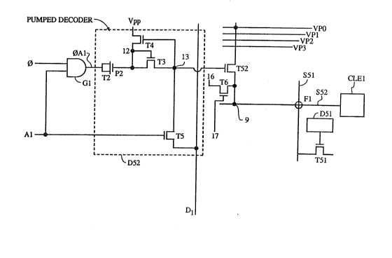
Fig. 6a shows antifuse F1 at the intersection of two
interconnect line segments S51 and S52. The antifuse is
10 programmed by providing sufficiently dif~erent voltages to
line segments S51 and S52 which in turn contact the two
terminals of antifuse F1. In an array in which the
invention is advantageously used, comprising line
segments, logic devices, and antifuses for interconnecting
15 line segments, a programming voltage can be applied to
each interconnect line segment of the array through a pass
transistor. According to the invention, one programming
pass transistor is provided for each interconnect line
segment. tMore than one antifuse may be and usually is
20 connected to one line segment, as will be discussed in
connection with Fig. 7a.) A programming bus to which
programming voltages can be applied extends through the
array, with each line segment in the array being
connectable through its pass transistor to one line of the
25 programming bus. In order to program an antifuse the two
terminals of the antifuse must be connected to line
segments which connect to different lines of the
programming bus.
As shown in Fig. 6a, line segment S51 is connected
30 through transistor T51 to programming voltage line VP1.
Line segment S52 is connected through transistor T52 to
programming voltage line VP0. Fig. 6a shows four
programming voltage lines VP0, VP1, VP2, and VP3 in the
programming bus. The antifuse is programmed by applying
_ g _
... .
.,
. ,. .. ~ . -
H\1223\P\APPOOl PATENr
suf~iciently different voltages to the two lines of the
programming bus which are connected through programming
transistors and corresponding line segments to the two
terminals of the antifuse, and turning on the programming
5 transistors while the voltages are applied to those
programming bus lines. Any voltac.~e can be applied to any
programming bus line; therefore the direction of current
flow through the antifuses such as Fl can be selected at
the time of programming.
10 NMOS Technology and Pum~ed Decoder
In a preferred embodiment, all programming voltage
transistors, such as T51 and T52, are NMOS transistors
having fairly large current carrying ability (typically 20
ma). Using only NMOS transistors has at least three
15 advantages over using mixed NMOS and PMOS transistors.
NM~S transistors have about twice the conductivity of PMOS
transistors, an important factor for the high current
needed to program antifuses. Further, it is possible to
pack adjacent transistors more closely when they are the
20 same conductivity type and space is not needed to separate
N-wells from P-wells. Finally, using only a single
conductivity type (N or P) simplifies the manufacturing
process.
The NMOS programming transistors are controlled by
25 pumped decoders such as D51 and D52, which apply a gate
voltage slightly higher than the programming voltage by
means discussed below, in order to allow the full
programming voltage and high current to be applied across
the antifuse. A pumped decoder allows low voltage address
30 and data signals to control programming of the antifuses
by pumping up the low voltage signals to higher
programming voltages.
In one embodiment, SRAM (static random access memory)
cells for configuring the array are included on the same
-- 10 --
:
,
;
M\1223\P\APPOOl ~ ~ ~; J ~ ~ ~ PATENT
chip as is the antifuse array. The SRAM cells require low
voltage (5 volt) address (row) and data (column) signals
for loading the SRAM cells with configuration information
at powër-up. It is most efficient to use the same address
5 and data lines which configure the SRAM cells to also
control programming of the antifuses. Advantageously,
this is possible with the present invention. The low
voltage signals which control the SRAM cells also address
pumped decoders which allow high programming voltages to
10 be applied to antifuses.
As shown in Fig. 6b, pumped decoder D52 of Fig. 6a
may be formed from transistors T2 through TS, transis~or
T2 having its source and drain commonly connected to act
as a capacitor. Also shown in Figure 6b are the elements -
15 shown in Figure 6a. The structure shown in Fig. 6b is
typically one element in an array of such structures, each
structure being addressed by a different combination of
address lines A0 through An to AN and da a lines D0
through Dm to DM. An array having such structures is
20 shown in Fig. 7a, and is discussed below.
Regarding the operation of the pumped decoder of Fig.
6b, a global clock signal ~, typically switching between 0
and 5 volts at a frequency on the order of 10 MHz, is
applied to AND gate G1. Global clock signal ~ generates a
25 row clock signal ~A1 when line Al is at logical one. To
allow the pumped decoder of Fig. 6b to pump up the voltage
on node 13, both of lines Al and D1 must be brought to a
logical one voltage level (5 volts).
When both lines A1 and D1 are addressed, the voltage
30 at node 13 is pumped up by clock signal ~Al alternately
pulling charge onto the gate of transistor T2, which is
acting as plat~ P2 of a capacitor, and then moving charge
to the gate of transistor T52.
The known pumped decoder circuit D52 of Fig. 6b will
35 now be explainecl. When logical one (5 volt) signals are
, . ,: : ~
H\1223\P\APP001 2 ~ ~ ~ 8 ~ ~PATENT
applied to address and data lines A1 and Dl, transistor T5
charges node 13 to roughly 4 volts (one threshold voltage
vt below the voltage on line Dl; threshold voltage is the
voltage difference between gate and source/drain o~ an MOS
5 transistor needed to turn on the transistor). Assuming
that ~A1 is at logical zero, capacitor plate P2 will have
charged to one Vt below node 13 through transistor T4. In
this quiescent state, current is not flowing through
transistors T2 through T5, though these transistors may be
10 on. Since A1 carries a logic one, as ~ rises from 0 to 5
volts, ~Al follows ~, and rises from 0 to 5 volts. As row
clock signal ~A1 rises, the rising voltage induces a
corresponding rise at node 12 through tha capacitor formed
by transistor T2. As node 12 rises above the threshold
15 ~oltage of transistor T3, transistor T3 turns on and
current flows from node 12 to node 13 (from plate P2 to
the gate of transistor T52). During this time transistor
T4 is off. When ~, and correspondingly, ~Al decrease from
5 volts to 0 volts, the capacitor formed by transistor T2
20 induces a decreasing voltage on node ~2. When the voltage
on node 12 approaches the voltage on node 13, transistor
T3 turns off. When the voltage on node 12 decreases more
than one Vt below node 13, transistor T4 turns on, thereby
transferring charge from Vpp to node 12. This completes a
25 pumping cycle. Typically tens or hundreds of cycles are
required to bring node 13 to its maximum high voltage
level, typically 17-18 volts. The maximum voltage at node
13 is determined by Vpp and transistor T4. As the voltage
at node 13 reaches one Vt above Vpp, current no longer
30 flows from node 12 to node 13 when transistor T3 is on,
but instead flows back to Vpp when transistor T4 is on.
Assuming the threshold voltage of transistor T4 is
the same as the threshold voltage of transistor T52, and
the supply voltage Vpp is the same as the high programming
- ~ . , - . :~ ,:
~1\1223\P\APPOOl ~ $ ~ $ PATENT
voltage VPo, transistor T52 will allow the full voltage
VP0 to be applied to node 9 for programming antifuse F1.
Note that supply voltage Vpp is not necessarily the same
as programming voltage VP0, since voltage VP0 may be low,
5 and the high programming voltage may be applied to the
other terminal of the antifuse.
After a node for addressing a transistor has been
pumped up, two different options may occur. Ths charge
may be held on the node for a period of time while the
lo transistor for accessing the other terminal of the
antifuse is addressed and turned on, or if the transistor
for addressing the opposite terminal is already on, the
node for addressing the transistor may be held high only
long enough for the antifuse to be programmed. The node
15 is then returned to a low voltage so that the transistor
i5 turned off. Sequential addressing of opposite antifuse
terminals is discussed below in connection with Fig. 7d.
In any case, charge is held on node 13 until antifuse Fl
has been programmed. The charge is held on node 13 (as -
20 discussed further below) by bringing line Al low before
bringing line Dl low. Node 13 is discharged by holding
line Al at 5 volts and bringing the global clock low while
Dl is brought low. In response, node 13 discharges
through transistor T5 to line Dl.
25 Application of the Structure and Method of the Present
Invention
Fig. 7a shows an array circuit in which the present
invention advantageously operates. Additional description
of configurable arrays and logic devices in which the
30 present invention advantageously operates may be found in
U.S. Patents 4,870,302, and 4,706,216, incorporated herein
by reference, and in "The Programmable Gate Array Data
Book" ~1989, available from Xilinx, Inc., 2100 Logic
Drive, San Jose, CA 95124, also incorporated herein by
- 13 -
1~1\1223\P\APPOOl ~ PATEHT
reference. As shown in Fig. 7a, a plurality of horizontal
and vertical interconnect line segments Ll through L54 are
positioned in an integrated circuit device with a
plurality of logic devices 9-1 through ~-6. Each
S interconnect line segment L1 through L54 is connected
through a programming transistor to a programming voltage
line VP0 through VP4, as shown in Fig. 6b. For
simplicity, only a few programming transistors, for
example TL41, and their associatecl pumped decoders, for
10 example DL41, are shown in Fig. 7a. Antifuses for
interconnecting line segments Ll t:hrough L54 are
positioned at many intersections of the line se~ments and
are represented as ~.
Also included in the array of Fig. 7a are
15 interconnection boxes J1 through J12. Within each of
these interconnection boxes are interconnect means,
preferably antifuses, for selectively interconnecting
lines which extend into the boxes. Fig. 7b shows
interconnection box J10, in which two lines enter from
20 each of the compass directions N, S, E, and W. Antifuses
allow each of these lines to be connected to each other
line extending into the box except for the other line
coming from the same direction. The twenty-four antifuses
shown in Fig. 7b allow this choice.
25 Proqramming Bus and Connections to Line_Segments
In order to program any of the antifuses, it must be
possible to provide the programming voltage across each
antifuse. As shown in Fig. 7b, each line segment N1, N2,
El, E2, S1, S2, W1 and W2 has a fixed connection through a
30 transistor to one of the lines VP0 through VP3 in the
programming bus. The programming bus must contain
sufficient lines that interconnect line segments feeding
opposite terminals of an antifuse are always connected to
different lines in the programming bus so that different
- 14 -
~ : ,. : . . .
:
;,
H\1223\P\APPOOl PATE!lr
voltages can be applied to the opposite terminals of each
antifuse. For a geometry in which lines enter a
connection region from four compass points, four
programming bus lines may be able to provide sufficient
5 flexibility to always connect opposite terminals of each
antifuse to different bus lines. However, if more varied
connection patterns will be used, additional programming
bus lines may be needed. A presently preferred embodiment
uses five lines in the programming bus. Additional
10 programming lines beyond four may program interconnect
lines which interconnect alternating logic devices, for
example. Five programming lines are shown in the
embodiment of Fig. 7a.
Fig. 7b shows an arrangement for programming the 24
15 antifuses to connect interconnect line segments in four
compass directions using a programming bus having four
lines (or using four lines of a larger programming bus).
~y allocating each of the four compass directions to a
different one of the four programming lines, it is
20 possible to provide the necessary voltage difference to
each of the 24 antifuses.
To program antifuse F1, segment N2 is connected to
programming bus line VP0 through transistor T811 by
addressing pumped decoder D811. (Addressing the decoders
25 will be discussed in connection with Figs. 7c and 7d.)
Segment W1 is connected to programming bus line VP3
through transistor T816 by addressing pumped decoder
D816. To connect segment N2 to segment W1 through
antifuse F1, while transistors T811 and T816 are on, a
30 first programming voltage is applied to programming
voltage line VP0 and a second programming voltage is
applied to programming voltage line VP3. There is
typically a preferred direction for applying these
programming voltages, depending on the makeup of the
35 antifuse. With the present invention, it is possible to
- 15 -
.
$ ~ ~
\1\1223\P~APP001 PAT~IT
apply the two programming voltages in either direction, or
indeed to apply sequential programming voltages of
opposite polarities.
Low Resistance of Proqrammed Antifuses
Because the voltages on the gates of transistors T811
and T816 are pumped higher by at least one threshold
voltage than the programming voltages applied to
programming lines vPo and VP3, the full voltage difference
applied to programming lines VP0 and VP3 will appear at
10 antifuse F1. Further, because the programming current
must pass through only the two transistors T811 and T816
and antifuse F1 between the major voltage source which
supplies the programming voltages and current, it is
possible to pass high current through transistors T811 and
15 T816 and antifuse Fl as antifuse F1 is being programmed.
The effect of the high current is to reduce resistance
between the two terminals of the antifuse. It is expected
that typical resistance of such programmed antifuses will
be on the order of 100 ohms.
Fig. 9 shows the relationship between the programming
current and the final resistance of an antifuse. At a low
programming current of some 4 mA, which cannot be exceeded
by prior art designs in which programming current may pass
through 5 to 8 transistors in series, resistance of the
25 programmed antifuse will remain on the order of 200 to 900
ohms. Such values of resistance have a significant
detrimental effect on circuit performance. The high
resistance of such prior art designs causes signal delay,
and the large spread in final resistance causes
30 unpredictability of ~he delay, which may cause
unacceptable circuit operation. By contrast, with the
present invention, in which programming current is on the
order of 15-20 mA, the approximately 100 ohm resistance of
programmed antiEuses is small in comparison with other
- 16 -
.
2~$`~
H\1223\P!APPOOl PATE!JT
resistances in the circuit, so that delay is both small
and predictable, and resulting circuit performance is
enhanced relative to the above described prior art.
Figs. 8A and 8B show programming circuits of the
5 prior art (Fig. 8A) and the present invention (Fig. 8B),
and contrast the serial nature of a prior art programming
circuit with the parallel nature of the present invention.
Programmed antifuses are indicated by a solid black dot.
As shown in Fig. 8A, when an antifuse is being programmed,
10 current flows in series through programming transistors
and the antifuse. For programming, a programming voltage,
on the order of 17 volts in the present example, is
applied to line segment 817, and ground voltage is applied
to line segment 821. To program antifuse F2, high
15 voltages, are applied to the gates of transistors TO, T1,
and T3, and a low voltage, zero volts, is applied to
transistor T2. The programming voltage applied across
antifus~ F2 will be at least one threshold voltage below
the voltage applied to the gates of transistors TO and Tl.
20 When a high programming current is flowing, this voltage
will also be lower than the voltage applied to segment 817
because of the resistance of transistors TO, Tl and T3.
It can be seen that when the device is scaled to provide a
larger number of transistors in series, the resistance of
25 these transistors can produce a significant decrease in
the current available for programming the desired
antifuse.
By contrast, as shown in Fig. 8B, antifuses FXo, FXI,
FX2, and FX3 are arranged in parallel between programming
30 voltage lines VPO and VP1. To program antifuse FX2,
current passes through only two transistors TX2 and TX3
regardless of how many antifuses are in the line and
regardless of which other antifuses have been programmed.
Advantageously, the use of a parallel programming
- 17 -
H\1223\P!APPOOl PATENT
arrangement such as shown in Fig. 8B results in a smaller
total silicon area (fewer and smaller programming
transistors) for a particular amount of resistance, or a
lower resistance for a particular silicon area.
5 Proqramminq Transistor Resistance Estimation
Just as antifuse programmed resistance will vary from
chip to chip, so also will the resistance of programming
transistors vary from chip to chip. It is possible to
obtain an improved estimate of on--resistance of the
10 programming transistors of a chip by providing one or more
pairs of test transistors manufactured by the same process
as the programming transistors but connected directly
between a pair of programming lines so that when the pair
of test transistors is turned on, the resistance of the
15 pair can be measured directly. It is presently considered
sufficient to provide only a single pair of test
transistors for determining the expected resistance of
programming transistors in the entire chip.
Programmed Antifuse Resistance Calculation
Further, with the arrangement of Fig. 8B, not only
can the programming current and voltage be high for a
resulting low antifuse on-resistance, but the resistance
of the programmed antifuse can be measured. If a low
voltage, say 1 volt, is applied to a programmed antifuse
25 by applying a logical one to the corresponding address and
data lines and applying 1 volt to one of the programming
lines and zero volts to the other programming line, the
programming transistors will operate in their linear range
(range in which resistance times current equals voltage).
30 Rasistance of the programming transistors can be closely
estimated as described below, so that the equation
V = I x (RTl + RF + RT2)
where V is the ~one volt) applied voltage,
- 18 -
; . ;
2 ~
1223\P\APP001 PATENT
RT1 and RT2 are the resistances of the corresponding
programming transistors when operating in the
linear range, and
RF is the on-resistanca of the programmed antifuse
5 can be solved for antifuse resistance, since all other
terms of the above equation are known or can be estimated.
Further, as can be seen in Fig. 9, à hiqh programming
current of 15-20 mA produces not only a low resistance but
a predictable resistance. The combination of low
10 resistance and predictable resistance makes it both
possible and less important to calculate the resistance of
a particular signal path. Antifuse resistance may be
calculated directly after the antifuse is programmed to
determine that the antifuse is ~unctioning properly.
lS Addressing Pumped Decoders
Fig. 7c shows an embodiment of the pumped decoder
addressing means. Vertical address lines D0 through D4
and horizontal address lines A0 throu~h A3 are shown.
Each pumped decoder is addressed by one vertical line and
20 one horizontal line. Also shown in Fig. 7c are four
interconnect line segments, horizontal interconnect line
segments X1 and X2 and vartical interconnect line segments
Y1 and Y2. At the intersections of these horizontal and
vertical line segments are four antifuses Fl-l, Fl-2, F2-1
25 and F2-2. Pumped decoder DX1, when addressed by address
lines A3 and D0, causes transistor TXl to turn on and
connect programming line VP0 to interconnect line segment
Xl. Pumped decoder DX2, when addressed by address lines
A2 and D0, causes transistor TX2 to turn on and connect
30 programming line VPl to interconnect line segment X2.
Pumped decoder DY1, when addressed by address lines A1 and
D2, causes transistor TY1 to turn on and connect
programming line VP3 to interconnect line segment Y1.
Pumped decoder DY2, when addressed by address lines A1 and
-- 19 --
.,
.: . .j: ,: -
~\1223\P\APP001
D3, causes transistor TY2 to turn on and connect
programming line VP2 to interconnect line segment Y2. To
program antifuse F1-1, transistors TX1 and TY1 are turned
on by applying high signals on address lines A3, D0, Al,
5 and D2, and while these two transistors ara on, applying
suf~iciently different programming voltages (typically 15
to 18 volts) to programming lines VP3 and VP0. From this
description it can be seen how the other four antifuses of
Fig. 7c are programmed, and inde!ed how antifuses in a
10 larger array are programmed.
Sequential Addressin~ and Hiqh capacitance Decoders
Fig. 7d shows an embodiment of the invention in which
another novel and useful feature is employed. Again,
assume antifuse F2-2 is to be programmed. In Fig. 7d,
15 just as in Fig. 7c, transistors TX2 and TY2 must be turned
on to program antifuse F2-2. In both Fig. 7c and Fig.
7d, transistors TX2 and TY2 are turned on by addressing
lines D2, A2, (for TX2) and Al, D3 (for transistor TY2).
Fig. 7c, however, shows a sparsa array in which these four
20 lines may be simultaneously addressed without also turning
on any additional transistors. However, with the array of
Fig. 7d, if the four lines D2, A2, A1, and D3 are
addressed simultaneously, the transistors for programming
antifus~ F1-2 are also turned on. The combination of
25 lines A1 and D2 turns on transistor TY1 in addition to the
desired result that the combination of lines A2 and D2
turns on transistor TX2.
It is desirable to be abla to use a compact array
such as shown in Fig. 7d in order to reduce silicon area.
30 A novel feature of the present invention allows antifuses
in such a compact array to be programmed without the above
ambiguity.
- 20 -
~ : .
;. : . -
: :
H\lZ23\P\APP001 PATE'lr
Sequential Addressinq of Antifuse Terminals
Instead of activating all four addresses of the two
line segments simultaneously, the line segments are
addressed in pairs sequentially, and the capacitance of
5 the decoder circuit used to hold the first addressed
programming transistor on until t:he second transistor has
been addressed and the antifuse programmed. There is no
possibility of addressing multiple antifuses, as occurs
when simultaneous addresses on address lines A1 and D2
10 cause the programming of antifuse Fl-2 (discussed above).
With the sequential addressing of the present invention,
as can be seen in Fig. 10, when antifuse F2-2 is to be
programmed, address lines Al and D2 are never addressed
simultaneously, so decoder DY1 never turns on transistor
15 TYl to apply a programming voltage across antifuse F1-2.
Programming of an antifuse requires only on the order
of one millisecond between the time programming voltages
are applied to lines in the programming bus and antifuse
programming is completed to achieve a typical resistance
20 on the order of 100 ohms. Y~t programming transistors
held on by their corresponding pumped decoders for a time
on the order of 10 ms after the corresponding address and
data lines are no longer addressed. Thus sequential
addressing of two programming transistors can be used to
25 cause only the desired transistors to be turned on so that
only the desired antifuse is programmed.
Timing for Sequential Addressing
For programming antifuse F2-2, assume that a high
voltage will be applied to interconnect line segment X2
30 and a low voltage will be applied to interconnect line
segment Y2. The timing sequence for this programming is
shown in Fig. 10. Re~erence numerals in Fig. 10 have the
same meaning as those in Fig. 7d. The decoder for the
line segment to which the low voltage will be applied is
- 21 -
~, ,: : : : :
H\1223\P\APP001 ~ PATENT
preferably addressed first, and for a sufficient number of
clock cycles to pump the decoder output node to its output
voltage. In this case, decoder DY2 for applying the low
voltage to line segment Y2 is addressed by applying
5 logical one (5 volt) voltages to address lines A1 and D3.
These logical one address voltag~es are applied for a
duration of less than one ms, causing the pumped decoder
to turn on transistor TY2 and thereby select line segment
Y2. As shown in Fig. 10, this takes on the order of 10 to
10 100 microseconds. Address lines A1 and D3 are then
deselected by placing logical zero first on line A1 and
then on line D3. (see Fig. 5b) The logical zero on line
A1 turns off transistor T5 and disables clock ~A1, thereby
isolating node 13 and retaining charge on the gate of
15 transistor T52.
Next, the decoder for the line segment to which the
high voltage will be applied is addressed. In this case,
decoder DX2 for line segment X2 is addressed by applying
logical 1 voltages to lines A2 and D3. This causes pumped
20 decoder DX2 (preferably of the type shown in Fig. 6b) to
raise the gate voltage on transistor TX2 to one threshold
voltage above ~he voltages on the Vpp line, turning on
transistor TX2 and selecting line segment X2. While line
segment X2 is addressed, the high and low programming
25 voltages are applied to the respective lines of the
programming bus. That is, a high voltage (15 to 18 volts)
is applied through programming bus line VP1 to line
segment X2 while zero volt levels are applied to
programming bus lines VP0, VP2, and VP3. The zero volt
30 level on VP2 is transferred by transistor TY2 to line Y2,
so that the programming voltage appears across antifuse
F2-2.
Initially, the full programming voltage appears
across the antifuse to be programmed, in this case
35 antifuse F2-2. As programming occurs, the resistance of
- 22 -
. . : ~
.
- . . .
- . .
.: . ~ -
$ ~ ~
~1\1223\P!APPOOl PATENT
the antifuse drops, current through the antifuse
increases, and the voltage difference across the antifuse
decreases.
When programming is complete, the programming voltage
5 is removed from the progra~ning bus, and addressing
voltages are removed from the second pair of address
lines. Completion of programming may be established by a
set time interval, by achieving an established programming
current, or by removing the programming voltage and
10 applying a voltage for measuring on-resistance (discussed
earlier).
Benefit of First Addressinq Low Voltage Line Segment
The reason the pumped decoder addressed first is
preferably that decoder used to apply the low voltage to
15 the antifuse, is that parasitic capacitance will tend to
hold the corresponding programming transistor on after
pumping ceases. Take the example shown in Fig. 7d of
programming antifuse F2-2 with a high voltage to line
segment X2 and a low voltage to line segment Y2. As
20 current begins to flow through antifuse F2-2, the voltage
on line segment Y2 approaches about 7 volts while the
voltage on line segment X2 approaches about 8-9 volts.
The voltage on plate Pl of parasitic capacitor CY2 will
rise as antifuse F2-2 begins to conduct. The rising
25 voltage on plate Pl induces a rising voltage on plate P2
of parasitic capacitor CY2. This rising voltage tends to
hold transistor TY2 on during the full programming cycle
even though pumped decoder DY2 is not being pumped when
antifuse F2-2 is being programmed. During the one to two
30 milliseconds in which this process takes place, the
voltage on the gate of transistor TX2 is pulled down by
the Miller capacitance of intrinsic capacitor CX2. But
this effect is overcome by the current source from pumped
decoder DX2 which is still addressed.
- 23 -
~ . .
H\1223~P\APPOOl ~ ~ `3~ PATE~T
With the sequential addressing of the present
invention, there is no possibility of an ambiguous
programming address, as was discussed above in which
simultaneous addresses on address lines Al and D2 could
5 cause the programming of antifuse F1-2, because as can be
seen in Fig. lo, when programminq antifuse F2-2, address
lines Al and D2 are never addressed simultaneously, so
decoder DYl never turns on transistor TYl to apply a
programming voltage across antifuse F1-2.
10 Global Clear Between Proqramminq of Successiva Antifuses
After programming an antifuse, in order to assure
that no programming transistors are inadvertently
addressed while the address is being moved from one
transistor to another, the programming transistors turn
15 off during a global clear operation (all address lines AO-
An of an array such as shown in Fig. 7d are brought high
and data lines DO-Dm are brought low during a transition
period), after which time tha next antifuse may ~e
programmed.
20 TestincT
Another benefit of the circuit of the present inven-
tion is that testing of logic devices and interconnect
lines (i.e., the programming logic circuitry) can be
parformed using the programming bus and address lines,
25 with no requirement for additional testing circuitry. As
can be seen in Figs. 6a and 6b and also in overview
Fig. 7a, certain lina segments extend to logic devices.
Each logic device must be tested for proper performance
before the device is shipped. However, the chip must be
30 able to be tested without programming any of the antifuses
available to the user, in order to make the full
programmability available to the customer who will use the
chip. Since certain of the interconnect lines connect
- 24 -
;` ,. ' `:~
,.. .
- -. : .
2~g~
H\1ZZ3\P!APPOOl PATENT
directly to a logic device and through a programming
transistor to one of the programming voltage lines, it is
possibla to use these programming transistors and
programming voltage lines to apply test vectors to the
5 logic davices. Any node in the antifuse array may be
tested by selectively turning on programming transistors.
For example, in Fig. 6a, by applying a test voltage to
programming line VPO, and turning on transistor T52, the
test voltage may be applied to logic device CLE1 without
10 the need for programming an antifuse~ Likewise, with the
logic array of Fig. 7a, various test signals may be
applied through various lines of the programming bus (not
shown in Fig. 7a) to lines L51 through L54 by turning on
appropriate programming transistors, thereby providing
15 test signals to logic device 9-5.
Test Modes
Three modes of testing can be performed using the
structure of the present invention, as shown in Fig. 6b,
for example.
A first testing mode, called row mode, can apply
logic signals to all interconnects and/or logic device
inputs addressed by a particular row of address lines Al
through An in the array. In row mode, described in the
summary above, the weak (resistive) pull-up transistors
25 such as T6 are turned on by applying a logical one to
nodes 16 and 17. Next, transistor T52 is selectively
turned on by applying logical one to lines A1 and D1,
which turns on transistor T5, and brings node 13 to
roughly 4 volts. Given that VPO through VP3 are all held
30 at zero volts, the 4 volt level on node 13 is sufficient
to hold trar.sistor T52 on and apply a logical zero to node
9 in spite of the waak pull-up from transistor T6. During
such test operations, the pump portion of pumped decoder
D52 is not used.
- 25 -
': ~
M~1223\P\APP001 2 ~
Node 9 of Fig. 6b is connected to an interconnect
line segment such as segments Xl, X2, Yl, or Y2 of
Figs. 7c and 7d or segments L1 through L54 of Fiq~ 7a. By
turning on an array of pull-up transistors such as
5 transistor T6 of Fig. 6b, then simultaneously turning on a
selected set of programming transistors such as TO of
Fig. 6b (or TXl, TX2, TYl, or TY2 of Fig. 7c and 7d) and
thereby applying pull-down voltages to certain programming
lines (such as Xl, X2, Y1, Y2 of Fig. 7c and 7d) lt is
lo possible to control through the addressing structure
(including lines Ao through A3 and DO through D4 of
Fig. 7c and 7d) which terminals of the logic devices
receive high and low input signals, thus providing test
vectors, without the need for separate testing lines for
15 each input terminal of a logic device. This set of
resistive pull-up transistors such as T6 provides pull-up
voltages to lines not interconnected in the programmed
logic array, and therefore serves the double purpose of
preventing floating lines during circuit operation and
20 providing a voltage source during testing. Row mode
allows loading of many address or data lines in parallel
so as to apply test vectors to a number of nodes
simultaneously.
In a second mode, called direct input drive mode,
25 node 13 is brought to 4 volts, as above. However, the
test signal is placed directly on VPO and this signal then
drives the logic device input at node 9 directly through
transistor T52. In this mode transistor T6 can be turned
off. By applying 5 volts to Vpp, the pumped decoder D52
30 can be used to raise the voltage at node 13 to
approximately 6 volts, thereby allowing the full rail to
rail signal on programming line VPO to be applied to the
logic device input at node 9. This mode can be used when
a single input needs to be driven at high speed.
In a third test mode, used for testing logic device
- 26 -
. . : , .. , : . :~
M\1223\P\,APP001 ~ PATENT
output signals, node 9 is an output node from a logic
device. In this mode, voltages at Al, Dl, 16 and 17 are
the same as in the second mode. However, line VPo is used
for detecting the signal applied by the logic device to
5 node 9.
Output of the logic devices on output line segments
L55 and L56 of logic device 9-5 (Fig. 7a) may be detected
by turning on appropriate programming transistors directly
connected to output line segments L55 and L56 of logic
10 device 9-5. In order to avoid programming any antifuses
during testing, the test voltages are typically 0 to 5
volts, much lower than the programming voltage of 15 to 18
volts which will program an antifuse.
Also preferably provided, though not specifically
15 shown in Fig. 6b, are antifuses which allow line segments
to be connected to high or low source voltages. This
option allows a constant high or constant low voltage to
be applied to any input terminal of a logic device not
used for a particular logic function, so that terminal is
20 not left floating.
Though only specific embodiments of the present
invention have been described here in detail, other
embodiments will become obvious to those skilled in the
art in light of the above description, and are intended to
25 fall within the scope of the present invention.
- 27 - i
.
,,
. .
: ~-''., ~;