Note: Descriptions are shown in the official language in which they were submitted.
B-30795
2 10 ~
~ LOCR-~OOP 8Y8TEN ~IT~ Y~T~RT.
BAN~W1~ AND ~GF. P~P PARAMETER~
C~ FIE~V OF ~ NV~N'l'10~
The present inventi3n pertains in general to a
freguency synthesizer having a phase loc:k loop system
which can be switched between a 510w ancl a ~ast transition
state by virtue of changing the performance
characteristics of the charge pump and the loop filter
elements.
' Exor~5s NRlaBI ïng~
Dote ot Depogil F'~h rll ~ ry 7 . I 9 9
I h~raby carlity that thb p~p~ or fe~ iri boin~ dap~
5ne~ h ~he U~it~d S~t~ Pogtnl Son~ "Expr~
M~il Post Otficu tD Addro~n ~ervi~ und~r 3? CF~
~.10 on ~he rlsto Indic~t~ and i~ ~Ds~d tD
tha Commiss!qr ~ ol P~tonu ~n~ lrr~d~ ~~~,
0231.
Sharone Hebert
~y~o~int~n~m~ ~ n r~i~a~r ~r ~)
~n~h~_ ~ ~J~
lSi~n~two ol Der~l n~ailine p9p~r or t~4~
2 2 ~ 7 5
BACgGRO~ND OF ~E lNv~lON
With radio frequency synthesizers and especially with
digital cellular telephones, it is desirable to have an
ability to switch between analog transmission and digital
transmission states. Present day analog radio systems,
such as analog cellular telephone systems, are not able to
transmit or receive digital signals because o~ the
frequency switching requirements of digital trans~ission.
In particular, the necessity in digital technolo~y that a
receiver or transmitt~r ~witch rapidly between different
frequencies requires that the circuitry be able to rapidly
stabili~e or "lock" guickly onto a particular frequency.
The need for fast frequency switching capabilities is
even more imperati~e in cellular telephone systems using
multiplexed digital technology where the synthesizer is
not only handling two basic communication channels (send
and recei~e), but is also handling an overhead channel
(where addltional information is transmitted, such as
location, signal strength, alternative cell sites, billing
information, etc.) as well as at least one additional
group of send, receive, and overhead frequencies. The
additional group(s) of frequencies is ~onitored in order
to determine when the communication link should be handed
o~f to another cell site with better signal strength.
Thus, an ability to switch frequencies is especially
important in the field of digital cellular communications
because the input reference signal frequency is ~requently
switched so that an alternative frequency signal from an
alternative cell site can be checked.
Present day analog systems are simply unable to lock
onto a new frequency quickly enough for digital
transmission requirements. Frequency ~witching
limitations in analog radios are imposed, in part, by the
design of the phase lock loop circuits, which are used in
CA 0206147~ 1998-08-2~
radio synthesizers to compare an incoming reference
signal to a local oscillating signal for the purpose of
locking the local signal to the input reference signal
and obtaining information from the phase shifts detected
between the two signals. Thus, phase lock loop circuits
are used in radio receivers to obtain information from an
incoming reference signal having a particular frequency.
Prior art frequency synthesizers utilize the phase
lock loop configuration shown in FIGURE 1 which includes
an input reference signal 1, a phase detector 2, a phase
lock loop filter 3, and a voltage controlled oscillator
(VCO) 4 coupled as shown in the drawing. Although there
are a number of different configurations for phase lock
loop filters, the description of the invention provided
herein is given with reference to the basic phase lock
loop filter configuration shown in FIGURE 1 which
includes a charge pump 3a and a second order R-C low pass
filter 3b. Such a configuration is suitable for analog
transmission, but is not suitable for frequency switching
required in digital transmissions. Of course, the
present invention can be implemented with loop filters
having a variety of configurations which differ from the
loop filter described herein.
It will be appreciated by those skilled in the art
that the frequency switching capability of the phase lock
loop circuit configuration shown in FIGURE 1 is improved
by improving (decreasing) the lock time, and that the
lock time for the phase lock loop frequency synthesizer
is improved by increasing the loop filter bandwidth Wn of
the phase lock loop circuitry. However, the loop filter
bandwidth Wn can only be increased to a point before
negative resistors are required in the filter 3b.
Because the phase lock loop filters as shown in
FIGURE 1 have only a limited ability to increase the
4 ~ 7 ~3
bandwidth Wn, present day ~nalog synthesizers cannot meet
the lock time, and there:~ore the ~requency switching,
requiremen~s OI digital transmission without the ~ddition
of complex circuitry or exten~ive reworking of the design.
5 2 ~
~MARY OF T~ v ~N'l'IO~
As will be explained below, the present invention
~elates to a phase lock loop circuit which can switch
quickly with frequency changes in the input re~er~nce
signal. In its regular or "analog" mode, the phase lock
loop of the present invention detects phase shifts in the
input reference signal in accordance with standard phase
lock loop operation. But when the input reference signal
changes frequenoy, the phase lock loop is switched into
its "digital" mode to enabl~ the cixcuit to quickly 1l lock"
onto the new frequency be~ore returning to the normal or
"analog" mode of operation. The present invention enables
the phase lock loop to lock quickly onto a new ~requency
by providing a "two-step" approach for increasing the loop
filter bandwidth Wn and therefore improving the lock time.
The first "step" maximizes the per~ormance o~ the filter
element, as limited by constraints imposed by the charge
pump and the overall phase lock loop synthesizer~ The
second step o~ the invention pushes bacX the constraints
imposed by the charge pump and phase lock loop
synthesizer, thereby enhancing the overall performance of
the synthesizer.
The phase lock loop filter o~ the present invention
includes a charge pump coupled to receive the phase error
signal from a phase detector for providing a phase lock
signal to a charge pump output node in response to the
phase error signal. The phase lock signal provided to the
output node i5 variable in response to a charge pum~
control signal in that charge is supplied or removed *rom
the rharge pump output nod2 at a given rate in response to
the phase error signal when the charge pump control signal
is in a first state, and is ~upplied or removed at a
different rate when the charge pump control signal is in a
second state. The phase lock loop filter also includes a
filter element coupled to the charge pump output node for
filtering the phase lock signal at a variable bandwidth,
said bandwidth being variably controlled by a filter
control signal. In operation o~ one embodiment of the
present invention, the charge pump control signal and
filter control signal are coupled together to a bandwidth
control signal so that the analog switches in the charge
pump and filter are activated and deactivated together.
In this way, when the rate of charge movement at the
charge pump output node is increased, the resulting signal
at the charge pump output node is ~iltered at a larger
bandwidth by the filter.
In an alternative ~mbodiment of the present
invention~ the charge pump oontrol signal and ~iltar
control signal are operated independently o~ one another
so tha~ only the current flow at the charge pump output
node is changed or so that only the bandwidth o~ the
filter element i~ changed. Independent operation of the
charge pump control signal and filter control signal may
be desired when operating in either analog or digital mode
and only limited improvement in the locX time is needed.
By reducing the "lock time" for a synthesizer, the
synthesizer's performance ability to switch between
~requencies is enhanced, and the synthesizer is thereby
improved. It is therefore desirable to have a frequency
synthesiz~r utilizing the standard phase lock loop
configuration which switches between frequencies with a
minimum lock time that is compatible with digital
transmission requirements. In particular, one embodiment
of the present invention utilizes the basic circuit
con~iguration used in analog c~llular radio transmission
to create a digital cellular radio transmitter/receiver,
thereby providing a cellular telephone system which can
operate in both analog and digital modes.
2 ~
BRIEF DE8CRIPT~ON OP T~E DRAWING8
For a more complete understanding of khe present
invention and the advantages ther20f, reference is now
made to the following description taken in conjunction
5, with the a~comr;~nying drawings in which:
FIGURE 1 is a block diagram of a basic phase lock
loop ~requency synthesizer having a phase lock loop filter
of standard design;
FIGURE 2 is an electric schematic diagram of an
embodiment of th~ present invention showing the ~ilter and
charg~ pump circuits;
FIGURE 3 is an alternative embodiment of the present
invention showing a different charge pump configuration;
and
FIGURE 4 is an alternative embodiment of the present
invention showing another charge pump configuration.
2 ~
- D~T~TT.~ DE~CRIPTION OF T~ iNv~lION
As was noted earlier~ the present invention is best
explained with refer~nce to the phase lock loop frequency
synthesizer ~or analog radio having the basic loop filter
confi~uration shown in ~IGUR~ 1. The loop filtsr
bandwidth WQ for the ba~ic con~iguration shown in FIGURE 1
is a function of the natural response W0 of the
synthesizer and the cutoff frequency Wl of the filter 3b
accor~ing tQ the equation Wn2 - W0W1 ~Equation No. 1).
With respect to the natural response W0p it will be
appreciated by those skilled in the art that the natural
response W0 is a function of the charge pump response K~
(volts/rad) and the voltage controlled oscillator response
Kv (rad/volt-sec) such that W0= ~ (Equation No. 2),
wher~ N is the divider factor ~or the operating frequency
to obtain the reference frequency as generated by the
divider which is coupled to the feedback input for the
phase detector (not shown). It will further be
appr~ciated by those skilled in the art that the cutoff
frequency W1 is a ~unction of the resistor values RA~ RB
and capacitor value C in the filter 3b such that
(RA + R~) C (E~UatiOn NO. 3) .
As will be explained below, the present invention is
actually a two-~tep improvement of the phase lock loop
frequency synthesizer shown in ~IGURE 1, the object of
which is to increase the loop filter ~andwidth Wn so that
the lock time for frequency switching is correspondin~ly
decreased. The ~irst step is to increas~ the loop filter
bandwidth Wn by adjusting the perform nce of filter 3b so
that the cut-off frequency W1 is increAsed. HoweYer, this
modification per~its only limited increases in the loop
filter bandwidth Wn beca~lse of constraints imposed by the
remainder of th~ phase lock 1QOP synthesizer. The second
CA 0206147~ 1998-08-2~
step of the invention "pushes back" these constraints,
thereby further enhancing the performance of the phase
lock loop synthesizer by further increasing the loop
filter bandwidth W~.
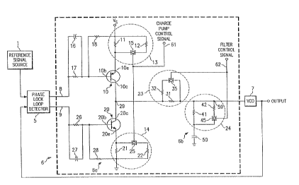
There is shown in FIGURE 2 a phase lock loop
frequency synthesizer according to one embodiment of the
present invention. The frequency synthesizer includes an
input reference signal source 1 for providing an input
reference signal; a phase detector 5 which is coupled to
receive the input reference signal and which is coupled
to receive a feedback signal from a voltage controlled
oscillator (VCO) 7 for providing a phase error signal; a
phase lock loop filter 6 coupled to the phase detector
for providing a steering signal;~and a voltage controlled
oscillator 7 coupled to the phase lock loop filter 6 to
provide a synthesizer output and a feedback signal to the
phase detector 5. Although the VCO output is shown in as
being the synthesizer output, the output may instead be
taken from the loop filter output node 59. The reference
signal source 1 provides an input signal to the frequency
synthesizer. It is the changes which occur in the
frequency of the input reference signal which the phase
lock loop circuit must quickly lock upon when digital
transmission occurs.
There are many types of phase detectors contemplated
as being within the scope of the present invention,
including phase detectors having a single output or a
plurality of outputs. Thus, the phase error signal from
the phase detector may consist of a single signal or a
number of signals, such as an error phase signal and a
reference phase signal. Clearly, the types of signalling
techniques for indicating a phase error will differ
between different phase detectors. In a preferred
embodiment of the present invention, the phase detector 5
lo 2~ 7~
includes two outputs, one for carrying an error phase
signal 8 and the other for carrying a reference phase
signal 9.
CQupled to receive the error phase signal 8 and
re~erence phase signal 9 from the phase detector 5 is a
charge pump 6a having a charge pu~p output node 29. The
charge pump 6a provide~ a phase lock signal to the charge
pump output node 29 which i6 coupled to the filter 6b.
The ~ilter element 6b i6 coupled through the loop filter
output node 59 to the VCO 7 which is in turn coupled to
the ~ynthesizer output and as a feedback signal to the
phase detector 5~
In accord~nce with the present invention, th2 loop
filter bandwidth Wn is increased by increasing the natural
lS response W0. The natural response W~ can be improved by
either changing the response K~ of the charge pum~ 6a or
by changin~ the response ~ of the VCO 7. Although charge
pumps, li~e phase detector~, are available in any of a
variety of configurations, any charge pump consists of at
least a source transistor coupled to a first voltage level
and a sink transistor coupled to the source transistor and
coupled further to a second voltage level. The ource and
sink transistors can be bipolar junction transi~tors,
~ield effect transistors, and indeed can be any "gate"
element which passes a signa} whPn properly activated.
Recognizing that the charge pump response K~ of the
charge pump 6a in FIGURE 2 is a function of the current
through the source transistor 10 (I~ou~ce) and 5ink
tra~sistor 20 (I~ink) of the charge pump when the
synthesizer ~requency is below the cutoff frequency Wl,
and in particular that K~ 5~ur~e ~ ~in~) /4~ the
present invention increases K~ (and accordingly ~ol~ ~Y
increasing the current through the source and drain
transistors 10, 20. This current increase is achieved by
CA 0206147~ 1998-08-2~
reducing the coupling resistance between the charge
pump's source and sink transistors 10, 20 and the
respective voltage levels or voltage supplies to which
these transistors are coupled. These coupling
resistances are described herein as a first switchable
resistor 13 and a second switchable resistor 14.
Although the switchable resistors are depicted and
described as being two resistors switchably coupled in
parallel to one another, any device having a defined
impedance is contemplated as being within the scope of
the claims, including transistors, and other impedance
means.
As shown in FIGURE 2, the charge pump 6a can be
switched between digital and analog operation by turning
the analog switches 15, 25 on or off. (In the following
description, the terms "emitter," "base" and "collector"
are all used with reference to transistors which are
bipolar junction transistors. If field effect
transistors, which are contemplated as being within the
scope of the present invention, are used to construct the
described circuitry, the terms "drain," "gate" and
"source" would be used instead.) In the analog mode, the
source transistor 10 is coupled through its emitter lOe
to a first switchable resistance 13 including first
resistor 11 and a first switched resistor 12 parallel-
coupled to the first resistor 11. The first switchable
resistance 13 is coupled to a voltage source Vs. The
collector terminal lOc of source transistor 10 is coupled
to the collector 20c of sink transistor 20 at charge pump
output node 29. The emitter 20e of the sink transistor
20 is coupled to ground through a second resistance 14
include second resistor 21 and second switched resistor
22 parallel-coupled to the second resistor 22. First and
second switched resistors 12, 22 are disconnected from
the charge pump 6a by the first and second analog
switches 15, 25
12 ~ 7~
which are turned off in response to the charge pump
control signal which is applied ~t lead 61. The error
phase signal output 8 ~rom the phase detector 5 is coupled
to th2 ~ource transistor 10 through the parallel coupled
capacitor 16 and resistor 17. Similarly, the reference
phase signal outpu~ 9 is coupled to the sink transistor 20
through parallel coupled resistor 26 and capacitor 27.
In order to switch the charge pump 6a into digital
mode, the analog switches 15, 25 are turned on by the
charge pump control signal at lead 61 so that the first
switched re5i5tor 12 iS connected in parallel across the
first resistor 11 and the second switched resistor 22 is
connected in parallel across the second resistor 21. The
parallel combination of the ~irst and second switched
resistors 12, 22 effectively reduces the emitter
resistance at the charge pump transistors, thereby
increasing W0 (and there~ore W~) by increasing the source
and sink current flow at charge pump output node 29.
In ~urther accordance with one embodiment of the
present invention, the filter 6b of the phase lock loop
filter 6 comprises a third switchable resistance 23
coupled to the charge pump 7a and to a loop filter output
node 59, and a series-~oupled fourth switchable resistance
24 and capacitor col~pled to the loop filter output node
59. The filter 6b is designed to operate in at least two
modes -~ analog operation and digital operation. In
analog operation, the switched resistors 32, 42 are
disconnected from the circuit by turning the analog
switches 35, 45 o~f so that the filter 6b consists only of
the ~ilter input resistor 31 and the series-coupled
resistor 41 and capacitor 50. In this mode, the filter 6b
functions as a low pass ~ilter suitable ~or analog
transmission. The phase locX signal ~rom the charge pump
13 2~
6a is thus filtered under a low pass filter having a
relatively small bandwidth when in the analog mode.
The loop filter bandwidth Wn can be ~urther increased
beyond the increase provided by the charge pump 6a by
reducing the resistance o~ the ~ilter 6b. In one
embodiment o~ tha pr~sent invention, Wn can be increased
by switching the filter 6b such that analog switches 35,
45 are turned on and the switched resistor~ 32, 42 are
connected in parallel to the filter input re~istor 31 and
the ~eries coupled resistor ~1, respectively. The analog
switches 35, 45 ~and there~ore, the parallel coupling of
the switched resistors 32, 42~ are activated in response
to the filter control signal applied at lead 62. In this
way, the resistance values of the filter 6b are reduced,
thereby increasing the cutoff frequency W1, according to
Eguation No. 3.
While this increase in the cutoff frequency W1 does
improve the loop filter bandwidth Wn (as seen through the
eguation Wn2 = WOWl~, the increase in the loop filter
20 . bandwidth Wn i~ limited by the parallel resistor
configuration in that W1 can only increase to a point
before negative resistor values are required for the
parallel~coupled resistors 31~ 32, 41, 420 In order to
obtain a lock tim~ on the order of two milliseconds or
less needed for digital application ~requency switching,
the present invention provides a novel impxoveme~t of the
filter 6b and charge pump 6a as described above.
As the rate of charge flow, or current, i~creases
through the charge pump transistors 10, 20, the natural
response W0 increases, thereby further increasing the loop
filter bandwidth Wn above and beyond the increase
permitted by only switchiny the resi~tors 32, 42 in the
filter 6b. In this way, loop fil~er bandwidth Wn is
increased significantly without requiring negative or
. 14 ~ 7 ~
negligible resistance values in the filter Çb and this
increase in the loop ~ilter bandwidth Wn permits frequency
switching to occur with lock times on the order of two
milliseconds or less.
Thus, the present invention p~ovides a phase locX
loop ~requency sy~thesizer having a reduced lock time for
frequency shifting. The improved lock time is achieve~ by
increasing the loop filter bandwidth W~. In or~er to
provide a Yariable loop filter bandwidth W~, khe cutoff
frequenoy Wl in the filter 6b can be ~ncrease~ upon
application o~ a filter control signal at lead 62, thereby
filtering the phase lock signal received from the charge
pump 6a at a higher bandwidth. In addition, the charge
pump 6a is designed to provide a phase locX signal to the
filter 6b in response to input from a phase ~etector 5.
The phase lock signal is varied upon application of a
charge pump control signal at lead 61 such that there is
more current at the charge pump output node 29 whsn in
digital mode with the analog switches 15, 25 turned on
2Q than when in analog mode with the switches 15, 25 turned
off. While the analog switches at the charge pump 6a and
filter 6b can be operated and controlled via cbarge pump
control signal and ~ilter control signal, these switches
can instead be coupled to and contrvlled by a single
bandwidth control signal such that the analog switches can
be activated or deactivated simultaneously.
In any event, the control signals may be generated
and applied under microprocessor control so that the
necessary switches are turned on when a ~re~ue~cy change
occurs ~o that the phase lock loop circuit can switch and
lock to the new frequency quickly. T:he microproce~sor may
~ctivate all the switches, or only some of the switches if
only a limited reduction in the lock time is needed. ~or
instance, the presenk invention also provides a benefit
15 ~ 7~
for straigAt analog radios where frPquency switohing
occurs when a call is handed off from one cell site to
~nother cell site. When such a hand o~f occurs, the
static burst which ~ometimes occurs upon the transition in
cell sites i~ 6ignificantiy reduced by improving the lock
time, even if only the charge pump switches are activated.
Alternatively, the microprocessor controller may only
activate the ~ilter ~witches to obtain the desired lock
time perfol ~nce.
An alternative embodi~ent of the present invantion is
shown in FIGURE 3 which includes a different charge pump
con~iguration utilizing the~charge pump response
modification and filter bandwidt~ modification of the
present invention. In particular, the phase detector 102
includes a single output 60 for providing a phase error
signal to the charge pump 103. The source transistor 80
and ~ink transistor 90 of the charge pump 103 are both
attached through their respective emitter terminals 80e,
90e to the phase detector output 60 to receive the phase
error signal; the base terminals 80b, 90b o~ the charge
pump tran~istors are both coupled to the charge pump
output node 71; and the charge p~mp resistor 70 is coupled
between the phase detector oukput 60 and charye pump
output 71. The source transistor 80 is coupled to a first
voltage level Vs through a first switchable resistance
comprising a first resistor 111 and a first switched
resistor 112. Sink transistor 90 is coupled to a second
voltage level ~ground) through second switchable
resistance comprising second resistor 121 and second
switchahle resistor 122.
In analog mode, the first switche~d resistor 112 and
~econd switched resistor 122 are not coupled to the charge
pump 103 because analog switches 115, 125 are turned off
in response to the bandwidth control signal applied ~t
16
~ lead 158. However, when the analog switches llS, 1~5 ~re
activated such that the ~irst switched resistor 112 and
second switched resistor 122 are connected in parallel to
the first resistor 111 and 6econd resistor 121,
respectively, the respon~e K~ of the charge pump 103 i~
increased, thereby increasing the response W0 and
correspondingly the loop Eilter bandwidth Wn which permits
faster locking times with ~requency chang~s.
The ~quation Wn~ = WOWl reveals how an increa~e in
the natural response W0 (which is a ~unction o~ the charye
pump response X~) increa~es the loop filter bandwidth Wn.
This same eguation also illustrates how an increase in the
cutoff frequency Wl (which is a function of the resistor
and capacitor values in the filter component of the phase
lock loop filter~, also increases the loop filter
bandwidth Wn. As can be seen ~rom FIGURE 3, the filter
104 is in the analog mode when the third resistsr 31 is
coupled to receive the phase lock signal from the charge
pump output node 71, and the series-coupled fourth
resistor 41 and capacitor 50 are coupled to the loop
~ilter output node 59 which is itself coupled to the thi.rd
re~istor 31. But in digital mode, the resistanca values
of the ~ilter 104 are reduced ~thereby increasing the
cuto~f fre~uency W1) by connecting in parallel third
switohed resistor 32 across third resistor 31 and fourth
switched resistor 42 to ~ourth resistor 41 in response to
the bandwidth control signal at lead 58.
The combined e~fect o~ switching the resistors 112,
122, 32, 42 in parallel to thç phase lock loop ~ilter
disclosed herein permits the loop filter bandwidth Wn to
increase so that the ~requ~ncy shifting can occur with a
lock time needed in digital applications.
The present invention is also shown in an alternative
embodiment depicted in ~IGURE 4 which includes an
17 2 ~ 7 ~
alternative charge pump configuration utilizing the charge
pump response modification of the present invention.
Source transistor 210 and sink transistor ~2~ are both
collector-coupled to the charge pump output node 229 for
supplyin~ and removing charge therefrom. The ~mitter 210e
of the source transistor 210 is coupled to a voltage
source through a first switchable resistance 213 including
first resistor 211 and ~irst switched resistor 212 which
is parallel-coupled to the first resistor 21~. Similarly,
the emitter 220e of 5ink transistor 220 is coupled to
ground throu~h the second switchable resistance 214
includin~ second resistor 221 and second switched resistor
222 parallel-coupled to second resistor 221.
Inverter transistors 201, 206 effectively invert the
signals at the outputs 98, ~9 from the phasP detector 105
in order to stabilize the charge removal and supply
~unction of the sink and source transistors 210, 2200 In
particular, transistor 201, whish is emitter ground~d~
receives the error phase signal from phase detector output
98 throu~h base resistor 208, thereby providing an
inverted signal to the emitter 210e o~ source transistor
210 through resistor 202. Transistor 206, which is also
emitter grounded, receives the reference phase signal from
phas~ detector output 99 through base resistor 205,
thereby inverting the reference phase signal provided to
the base 220b of sink translstor 220~
As can be seen ~rom FIGURE 4, the base 220b of the
sink transistor 220 and the collector o~ the inverter
transistor 206 are both coupled to a voltage sourcQ V~
through resistor 207, and ara ~urther coupled to ground
through the series-coupled resistor 228 and diode 227
which provides diode compensation ~or the sink transistor
220. Similarly, diode compensation is provided ko the
source transistor 210 through the sPries-coupled resistor
CA 0206147~ 1998-08-2
18
218 and diode 217 which are coupled between the voltage
source Vs and the base 210b of the source transistor 210
which is further coupled to ground through resistor 209.
Each of the analog switches 215, 225 which connect
the first and second switched resistors 212, 222 in
parallel to the first and second resistors 211, 221 are
controlled by the charge pump control signal at lead 61
so that the rate of charge movement at charge pump output
node 229 (also referred to as the phase lock signal) is
10 faster when the switches 215, 225 are activated than when
deactivated. In this way, the phase lock signal provided
by the charge pump 108 to the filter 109 is variable in
response to the charge pump control signal.
The present invention provides for reduced lock
times in frequency switching by modifying the natural
response W0 and charge pump response K~ with switchable
two-state resistors wherein each two-state resistor
consists of a primary resistor and a switched secondary
resistor which is coupled in parallel to the primary
resistor in response to a charge pump control signal,
filter control signal or bandwidth control signal,
whatever the case may be. It will be appreciated that
the present invention encompasses the use of any element
having two programmable impedance values greater than
zero which can be selected in response to a control
signal.
Although several embodiments of the invention have
been illustrated in the accompanying drawings and
described in the foregoing Detailed Description, it will
be understood that the invention is not limited to the
embodiments disclosed, but is capable of numerous
rearrangements, modifications and substitutions without
departing from the scope of the invention.