Note: Descriptions are shown in the official language in which they were submitted.
2Q ~5~
DEPOSITION OF TUNGSTEN
FIELD OF THE INVENTION
This invention relates to a method of deposition of
tungsten and tungsten metallization for integrated
circuits.
BACKGROUND OF THE INVENTION
In fabrication of CMOS devices for VLSI integrated
circuits, tungsten is a preferred alternative to
conventional aluminium (Al) alloys for metal interconnect
and for submicron contacts and vias, particularly where
high current density is required. As device ~;m~n~ions
become smaller and the packing density of high speed
devices increases, reduced metallization linewidth requires
the formation of smaller contacts and vias with vertical
sidewalls. In use of tungsten for contacts and vias,
tungsten has high resistance to electromigration, provides
superior step coverage and does not form hillocks. On the
~other hand, thin layers of tungsten have a higher sheet
resistance than conventional aluminium alloys. For
example, for use of tungsten as interconnect metallization,
deposition of a film of about l~m thickness of tungsten may
be required to provide the desired resistivity, of 8-9~Qcm,
typically ~ 8.3~Qcm.
A thin film of tungsten may be formed by chemical
vapour deposition (CVD). In a conventional CVD process,
tungsten hexafluoride, WF6, is reduced by hydrogen, H2, in
argon carrier gas, at a pressure of ~l Torr. The superior
step coverage of CVD tungsten film, relative to sputtered
aluminium alloys, provides that vias and contact holes can
be filled by blanket deposition of tungsten overall and
subsequent etching back of excess tungsten to leave
tungsten only in contact holes and vias. In this scheme,
aluminium is used as metal interconnect. In use of
tungsten for interconnect applications, a conformal CVD
tungsten film may be deposited which is capable of filling
holes having high aspect ratios and providing contact plugs
in vertical walled contact holes.
2 ~ ~7~
Tungsten does not adhere well to common dielectric
materials, including silicon dioxide SiO2. Satisfactory
adhesion to the substrate is required for tungsten films
both for filling of contact and via openings and for use of
tungsten as interconnect. A known method of improving the
adhesion of tungsten to substrate is deposition of an
adhesion layer, for example TiN or TiW, before deposition
of tungsten. The adhesion layer allows for formation of
strong chemical bonds between layers of tungsten and a
lo dielectric such as SiO2.
Known processes for deposition of films of tungsten
metallization of l~m thickness and having the desired
resistivity produce films with a rough surface and high
film stress. During deposition of thin tungsten films
<2000A) using a conventional CVD process, in which WF6 is
reduced by H2 in argon carrier gas, at a pressure of ~1
Torr, the tungsten film initially has small grains, but the
grains grow and form long columnar grains in the growth
direction as film thickness increases. The columnar grains
have pyramidal caps forming the surface of the film.
Consequently, the resulting film has a rough surface.
Also, film of this structure has a tensile film stress of
-101~ dyne/cm2. This stress is much greater than that
desirable to match, or compensate, the film stress of an
underlying film of dielectric, such as SiO2, which typically
has a compressive film stress of ~ 2 x 10⁹ dynes/cm2.
Surface roughness of tungsten films deposited by
known CVD processes increases with increasing film
thickness. Surface roughness affects the optical
properties of the film and reduces specular reflectivity
(and conversely increases diffuse reflectivity) in the
spectral region used for photo-lithography (around 436nm).
The recognition of alignment marks may be repeatable and
accurate only for a film thickness less than 5000A.
Typical tungsten film of ~8000A thickness, deposited by
known CVD processes which provides good step coverage, has
a specular reflectivity of 20% or less compared to a
.
silicon reference wafer. When the specular reflectivity of
a rough film is reduced to such an extent, or if surface
roughness is significant enough to obscure alignment marks,
subsequent photo-lithographic alignment for patterning of
interconnect structure is impossible. Consequently use of
thick tungsten films for interconnects is impracticable.
Another disadvantage of conventional processes for
deposition of a thin film of tungsten on silicon by
reduction of WF6 with hydrogen results from a significant
lo amount of volatile products such as HF, and the presence of
WFX species, which attack the underlying silicon, and result
in undesirable etching and pitting of the silicon surface
during deposition.
In another known method of chemical vapour
deposition of tungsten by reduction of WF6 with silane it is
found that there is reduced pitting and etching of a
silicon substrate. A higher rate of deposition may be
obtained by reduction of WF6 with silane instead of
hydrogen. The resulting tungsten film has a smoother
surface. However, the resulting film has poor step
coverage, and adhesion to the underlying silicon is
inferior. Poor adhesion may result in problems such as
lifting of the film and particulate contamination, as well
as poor electrical performance and reliability.
To improve adhesion, U.S. Patent 5,028,565 to Chang
et al. for example, describes use of an adhesion layer,
followed by deposition of a thin nucleation layer of
tungsten before deposition of the major thickness of
tungsten by a method of CVD of tungsten using a conven-
tional mixture of reactive gases including WF6, H2, in a
carrier gas of argon, carried out in the presence of
nitrogen. The '565 patent discloses that deposition in the
presence of nitrogen and at higher pressures up to 760
Torr, preferably at ~80 Torr, together with high gas flow
rates, and elevated temperature, 450-475~C, resulted in
smoother tungsten films. The resulting tungsten film
showed increased specular reflectivity of the deposited
~7~
tungsten surface, near 100% relative to silicon, which
facilitated to use of photolithography in the subsequent
patterning step. However, when the tungsten deposition was
carried out in the presence of nitrogen at low pressure, at
10 Torr, the specular reflectivity of the tungsten film was
reduced to only 20%. The increased pressure, together with
high gas flow rates and increased temperature, resulted not
only in a tungsten film having a smoother surface, but also
in increased tungsten deposition rates by up to an order of
magnitude (2000-7000A/min) compared with conventional known
methods (~ 30A/min).
On the other hand, as a practical matter, it is not
possible to operate many known CVD reactors at the higher
pressures, >80 Torr, required for the method disclosed in
the '565 Patent to Chang to achieve deposition of tungsten
films having a smooth surface suitable for interconnect.
Thus, practical difficulties are encountered in using low
pressure CVD to provide tungsten films having good
adhesion, a smooth surface for use as interconnect and
satisfactory step coverage for filling contact via holes.
SUMMARY OF THE INVENTION
The present invention seeks to provide a method of
depositing tungsten and a method of providing tungsten
metallization for integrated circuits in which the above-
mentioned problems are reduced or avoided.
According to one aspect of the present invention,
there is provided a method for chemical vapour deposition
of tungsten for an integrated circuit, comprising:
exposing a substrate to a mixture of reactive gases
consisting of WF6, H2 and a carrier gas consisting
essentially of nitrogen, maintaining a pressure between 1
and 9 Torr, a deposition temperature between 430C and 500C,
and controlling the relative flow rates of H2 and WE6 to
1. ~
provide a H2/WF6 flow rate ratio of between 5 and 30, the
mixture of gases thereby depositing on the substrate a
layer of tungsten having a smooth surface.
By deposition of tungsten by CVD in the absence of
argon or other inert gas, but in the presence of a carrier
gas which is known to adsorb on tungsten, and which is
substantially unreactive in the gas phase, it was found
that the surface roughness of deposited tungsten film was
significantly reduced over range of flow rates and
pressures of the reactive gases.
The carrier gas is a gas which adsorbs by
chemisorption on tungsten, preferably nitrogen. Smooth
films of tungsten were obtained in the temperature range
from about 430C to 500C, and advantageously, film stress
was reduced for deposition at a higher end of this
temperature range. However, the preferred deposition
temperature is 480C to avoid excessive thermal diffusion
effects in the substrate. High deposition rates were
obtained at a low pressure, ~9 Torr, and low gas flow
rates, and the resulting films had low film stresses.
Advantageously, a minor proportion of SiH4, e.g. 15
sccm, is added to the reaction gases to increase the
deposition rate of tungsten.
Preferably, a first thickness of tungsten is deposited
while maintaining a H2/WF6 flow rate ratio between 6 and 9
to provide good step coverage on the substrate, and
subsequently increasing the H2/WF6 flow rate ration between
20 and 30, and depositing a second thickness of tungsten,
thereby forming a layer of tungsten having a smooth
surface.
According to another aspect of the invention, there is
provided a method of chemical vapour deposition for forming
a layer of tungsten for metallization for an integrated
circuit, the method comprising:
exposing the substrate to a reactive gas mixture
consisting of WF6, H2, and a carrier gas, maintaining a
pressure from several mTorr to 10 Torr, and a temperature
between 430C and 500C, and controlling the gas flow rates
to provide from 10 to 40 sccm WF6 and gas flow rate ratio
of H2/WF6 in the range 5 to 30, thereby depositing a layer
of tungsten in at least two steps comprising:
in a first step, selecting a carrier gas consisting
essentially of an inert gas, and depositing a first
thickness of tungsten having good step coverage on the
substrate, and in a second step, after changing the carrier
gas to consist essentially of nitrogen, depositing a second
thickness of tungsten having a smooth surface.
Preferably, the layer of the first thickness of
tungsten is deposited by hydrogen reduction of WF6 in a
carrier gas comprising argon or nitrogen, with a H2/WF6
ratio between 6 and 9 to provide good step coverage of
>60%. Advantageously, the layer of the second thickness of
tungsten is deposited by hydrogen reduction of WF6 in
nitrogen and in the absence of argon, with a H2/WF6 ratio
increased to be in the range of 20 to 30 to produce a
tungsten layer having a smaller grain size, and smoother
surface, to ensure low diffuse reflectivity. Beneficially,
a minor proportion of silane is added to the reactive gas
mixture to increase the deposition rate and further reduce
the surface roughness. thus, a multi-step deposition
process provides tungsten metallization having a smooth
surface, low stress and good step coverage. Since the
desired properties of a tungsten film depend on its
application, the tungsten film used for filing contact and
via openings requires excellent step coverage ~90% and good
deposition uniformity but large grain sizes and high stress
may be tolerated. In contrast, the surface layer of
tungsten forming interconnect structures has a smooth
~7~
surface (i.e. small grain size) to facilitate
photolithography, low resistivity, and low film stress,
and, where interconnect is deposited on at least partially
planarized topography, lower step coverage is acceptable.
Thus, the present invention provides a method of
depositing tungsten and a method of forming tungsten
metallization for an integrated circuit which reduce or
overcome the above mentioned problems.
BRIEF DESCRIPTION OF THE DRAWINGS
Embodiments of the invention will now be described by
way of example, with reference to the accompanying
drawings, in which:
Figure la -le shows a schematic cross-sectional view
of part of an integrated circuit structure at successive
stages in a method of deposition of tungsten according to a
first embodiment of the present invention.
Figure 2a - 2e shows a schematic cross-sectional view
of part of an integrated circuit structure at successive
stages in a method of deposition of tungsten according to a
second embodiment of the present invention.
Figures 3 to 8 show graphs of the effects of varying
process parameters on the characteristics of tungsten films
deposited by the method according to the first embodiment
of the present invention.
DESCRIPTION OF THE PREFERRED EMBODIMENTS
In a method of deposition of tungsten according to
embodiments of the present invention, as described below, a
layer of tungsten for metallization of an integrated
circuit was deposited in a conventional CVD apparatus which
comprised a Varian 5101 cold wall, low pressure CVD reactor
system. The wall of the reactor chamber was kept at a
,.
, ...
8 ~ ~ ~ 7 ~
temperature around 17~C to minimise the deposition of
tungsten at the wall. The system was furnished with a
loadlock connected to a turbomolecular pump to achieve a
base pressure of approximately 10-6 Torr in the chamber.
A substrate, in the form of a semiconductor silicon
wafer, was clamped to a graphite chuck within the reactor
chamber, with the wafer surface facing downwards, and was
heated radiantly, with eight halogen lamps to a desired
processing temperature. A thermocouple was located in the
o chuck to monitor the chuck temperature. To maintain good
heating uniformity the diameter of the graphite chuck was
larger (250mm) than the wafer diameter (for lOOmm and 150mm
wafers) and a temperature gradient of not more than 10~C
was maintained across the wafer diameter.
A mixture of reactant gases comprising WF6, H2, and
a selected carrier gas was introduced at controlled flow
rates into the reactor chamber through a gas delivery
system comprising a tube with small holes located at the
bottom of the reactor. The reacting gases were uniformly
distributed using a diffusion plate located at about lOOmm
from the tube. The diffusion plate controls the uniformity
of the film thickness across the wafer: the distance
between the diffusion plate and the wafer controls the
fluid dynamics of the reactant gas mixture and hence the
distribution of reacting species at the surface of the
wafer to provide for uniform deposition of a layer of
tungsten over the surface of the wafer.
Deposition was carried out at temperatures in the
range from 350-600 C and at pressures in the range from
several mTorr to 10 Torr.
Gas flow rates were controlled to provide gas
mixtures having a predetermined H2/WF6 ratio and flow rates
measured in sccm (standard cubic centimetres per minute),
as follows: WF6 10-40 sccm and H2 240-800 sccm to provide a
H2/WF6 ratio between 5 and 30; SiH4 flow rate 0-15 sccm; in a
carrier gas comprising nitrogen or an inert gas at a flow
rate of ~90 sccm.
9 ~ 5 1
In a method according to a first embodiment of the
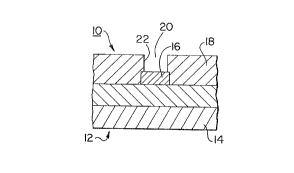
invention, a tungsten film was deposited on a substrate 12
comprising a silicon semiconductor wafer 14 having parts of
a partially fabricated integrated circuit defined thereon,
including a first conductive layer 16 and an overlying
surface layer 18 of a insulating dielectric material
defining steep-sided via holes 20 therethrough (Figure 1
a). The via holes 20 are provided by a conventional known
method, for example, after chemical vapour deposition of a
o dielectric layer 18 of silicon dioxide, the layer 18 was
coated with resist material, patterned and anisotropically
etched to define contact via holes 20 having steep side
walls 22. After stripping the resist, the substrate was
coated with a thin layer (~800A) of TiN 24 to provide an
adhesion layer (Figure lb). The TiN coating 24 was
deposited by a conventional known method, i.e. sputtering.
A thin nucleation layer 26 of tungsten was then
deposited over the adhesion layer by CVD reduction of
tungsten hexafluoride with hydrogen. The wafer was
preheated to 480 C in a non-reactive gas, e.g. nitrogen,
for 120 seconds at a pressure of 100 mTorr, flow rate of 90
sccm. A reactive gas mixture comprising H2, WF6 and SiH4 in
a carrier gas of nitrogen was then introduced into the
reaction chamber at a controlled, low flow rate to provide
a predetermined ratio of H2/WF6 so as to deposit a thin
layer of -lOOOA of tungsten on the substrate (Figure 1 b).
For example, the resulting nucleation layer of tungsten has
good adhesion and good step coverage (>60%) when deposited
on the substrate by hydrogen reduction of WF6 at a high
H2/WF6 ratio, ~20 to 25, and in the presence of a low
partial pressure of SiH4 (~5sccm) and at a total pressure of
~100 mTorr. In deposition of the adhesion layer, the
presence of silane did not degrade the step coverage, at
the expense of adhesion, and silane flow rates above 10
sccm significantly degraded adhesion. As an example,
process parameters are listed in Example 1, step 2 in which
a preferred flow rate was 4 sccm of silane and a H2/WF6
ratio of 25, with 90 sccm of nitrogen at a total pressure
of 250mTorr.
After deposition of the adhesion layer 24 the flow
rates of the reactive gas mixture was changed and a layer
of a first thickness of tungsten 28 was deposited (Figure 1
c). About 5000A tungsten was deposited using a low H2/WF6
ratio of about 6 to 8, and 0 to 15 sccm of silane, in
nitrogen, at a total pressure of ~9 Torr, to a sufficient
thickness to fill the contact vias. The first thickness of
o tungsten 28 forms tungsten plugs which fill the via holes
with high step coverage. Advantageously, a film having a
step coverage >60% is provided to substantially fill steep-
sided vias using the process parameters listed in Example
1, step 3.
After deposition of the first thickness of tungsten
28, the flow rates of the reactive gas mixture are changed
to increase H2/WF6 ratio to ~20, with 0 to 15 sccm of
silane, while maintaining the total pressure at ~9 Torr. A
layer of a second thickness of tungsten 30 is then
20 deposited under conditions that result in a film having a
smaller grain size, and a smoother surface, As an example,
suitable process parameters are listed in Example 1, step
4. A second thickness 30 of ~5000A of tungsten was
provided having a smaller grain size than the first
thickness, and having a smooth surface, characterised by a
low diffuse reflectivity and high specular reflectivity, to
form a conductive layer which may be photo-lithographically
patterned to define interconnect structures, i.e.
conductive metal lines of the integrated circuit.
Thus, tungsten metallization for an integrated
circuit was formed by depositing layers of tungsten in
stages of a process in which the mixture of reactant gases
was sequentially changed to control the structure and
characteristics of the resulting tungsten layer. After
deposition of a thin nucleation layer of tungsten having
good adhesion to the substrate, a layer 28 of first
thickness of tungsten having good step coverage was
,
deposited filling via holes 20 with tungsten.
Subsequently, the reactant gas mixture was changed and
tungsten was deposited overall to provide a layer of a
second thickness of tungsten having a smooth surface, with
low diffuse reflectivity which may be lithographically
patterned for defining interconnect structures.
The step coverage of the 5000A layer of tungsten
filling the vias was >60% and the film stress when
deposited at 480 C are acceptable. In deposition of the
o interconnect layer the H2/WF6 ratio was increased to ~20, to
ensure low diffuse reflectivity, i.e. a smooth surface to
the tungsten interconnect film. The step coverage was
lower, at ~40%, but this is satisfactory, because the
contact via holes are almost filled with the first
thickness of tungsten deposited.
The effect of varying the deposition parameters,
i.e. the pressure, gas flows, flow ratios of the reactive
gases and deposition temperature on the characteristics of
the resulting tungsten films are shown in the graphs of
Figures 3 to 8. The graphs show the characteristics of
films of tungsten including specular and diffuse
reflectivity, film stress, as a function of pressure, gas
flow rate ratios, temperature and film thickness. For
comparison, the graphs show data relating to the
characteristics of tungsten films deposited in a nitrogen
carrier gas, as described above, and also for tungsten
films deposited under the same conditions as in Example 1,
but substituting argon (~9Osccm, see Example 3), a
conventional inert carrier gas, instead of nitrogen.
The surface roughness of the resulting tungsten
films was evaluated by measurement of specular reflectivity
relative to bare silicon wafers and diffuse reflectivity of
light at ~436nm. Surface roughness and step coverage were
investigated by scanning electron microscopy.
It was observed that replacing an inert carrier
gas with nitrogen resulted in a very significant reduction
12
in surface roughness and film stress of the deposited
tungsten film (Figures 3 to 8).
The films deposited in the presence of nitrogen
were characterised by a higher specular reflectivity and
lower diffuse reflectivity, resulting from a smoother film
surface (Figure 3). An improvement in specular
reflectivity was observed on increasing the deposition
temperature from 430 C to 500'C (Figure 3) and in
increasing the pressure from 1 to 9 Torr (Figure 4). At
o film thicknesses 21~m, films deposited in a nitrogen
carrier gas showed specular reflectivities over 90%
compared with less than 60% for tungsten films deposited in
the presence of argon.
The H2/WF6 ratio in the reactant gas mixture also
had a very significant effect on the film structure (Figure
6). The H2/WF6 ratio was varied while the total flow rate
was maintained constant by changing the flow rate of
nitrogen. In the absence of argon in the carrier gas,
increasing the H2/WF6 ratio from 5 to 20 was found to
increase the specular reflectivity significantly from 70%
to over 90% and decrease the diffuse reflectivity of the
resulting tungsten film from ~45% to <30%.
Satisfactory photo-lithographic alignment was
made on tungsten films having diffuse reflectivities of
less than 15%. Diffuse reflectivities less than 15% were
obtained for tungsten films over ~l~m thick (Figure 5).
For comparison, diffuse reflectivity of less than 8% is
typically required for satisfactory alignment for photo-
lithography on aluminium alloy.
Film stress was measured on an FSM 8800 Model 81006
system. A bare silicon test wafer was coated with 800A of
sputtered TiN as an adhesion layer and the radius of
curvature was measured. The wafer was then coated with a
desired thickness of tungsten film and the curvature was
measured again. The film stress of the tungsten film was
calculated from the change in radius of curvature.
13 ~ R ~ ~ 5 ~ ~
Advantageously, the film stress of thicker films of
tungsten was significantly lower for tungsten films
deposited from reaction in the presence of nitrogen
compared with argon (Figure 8). Deposition at higher
temperatures (Figure 7) was also beneficial in reducing the
film stress. The film stress was a weak function of the
H2/WF6 ratio and the pressure. A tungsten film deposited at
480~C in N2 has comparable film stress to a sputtered
aluminium film of the same thickness.
Addition of silane to the reaction mixture
increased the deposition rate and increased the specular
reflectivity of the surface.
During deposition of the nucleation layer in step
2, to reduce Si substrate damage by reaction of WF6 or
fluorine by-products with silicon it was advantageous to
increase SiH4 flow, lower the deposition temperature and
reduce the total pressure. Under the conditions listed as
Example 1, step 2 ("pre-deposition") the predominant
reaction was reduction of WF6 by silane. However,
20 increasing the partial pressure of SiH4 in increasing the
flow rate from 4 to 15 sccm at this stage of the tungsten
deposition degraded the adhesion of the tungsten film to
the substrate.
For deposition of the surface layer of tungsten for
interconnect in the presence of nitrogen (Example 1), the
diffuse reflectivity increased from 5% to 10% with increase
of film thickness from 7000A to 10,000A. On the other
hand, the diffuse reflectivity of tungsten film deposited
in the presence of argon (Example 3) increased from 5% to
22% with increase in film thickness from 4000A to 10,000A.
The addition of silane to the reaction mixture
increases the deposition rate from, e.g. from 3800A/min to
4900A/min, and reduces surface roughness. The diffuse
reflectivity was reduced by ~10% in the presence of silane
(4 sccm). The moderate step coverage (~40%) of the surface
layer was adequate, because the via hole is almost filled
14
by the deposition of the first 5000A of tungsten. The film
stress was not sensitive to the H2/WF6 ratio.
Thus, a composite structure of layers of tungsten
having different characteristics together provide tungsten
metallization for an integrated circuit having a low
surface diffuse reflectivity, low stress and excellent step
coverage in via holes.
The resulting surface layer of tungsten may be
patterned and etched by a conventional known method, for
0 example by reactive ion etching by exposure to a plasma
generated from SF6.
Advantageously, nitrogen flow between the wafer and
the graphite chuck during deposition of tungsten reduced
amount of deposition of tungsten on the back side of the
wafer. An additional process step of dry etching by a
conventional method, for example by exposure to a plasma
generated from SF6, may be used to remove excess tungsten
from backside of the wafer if required.
In forming interconnect for integrated circuits, to
provide good adhesion to a substrate comprising an
insulating layer such as silicon dioxide, an adhesion layer
such as TiN, is desirable for the successful nucleation of
the blanket tungsten film. Sputtered TiN was found to be
thermally stable, has good step coverage, low contact
resistance and good etching properties. Other materials
suitable as adhesion layers include Ti, TiW, Ti/TiN, MoSi2
or Wsi2-
In a method of depositing tungsten according to asecond embodiment of the invention, a tungsten film was
deposited on a substrate 12 comprising a silicon
semiconductor wafer 14, similar to that used in the first
embodiment (Figure 2). The same reference numerals are
used for defining similar parts of the structures shown in
Figure 2 and Figure 1. Process conditions are listed as
Example 2. The substrate 12 has parts of a partially
fabricated integrated circuit defined thereon, including a
dielectric insulating layer of silicon dioxide 18 defining
1;''~
~ 9'
steep sided via holes 20 exposing a conductive layer of
metal 16 therein. The first and second steps of depositing
an adhesion layer 24 of ~800A TiN and a nucleation layer 26
of ~lOOOA of tungsten were carried out as described for the
first embodiment, but substituting argon for nitrogen as
the carrier gas (Example 2, steps 1 and 2).
After deposition of the adhesion layer 24 and the
nucleation layer 26 the flow rates of the reactive gas
mixture was changed and a layer of a first thickness of
lo tungsten 40 was deposited (Figure 2 c). About 5000A
tungsten was deposited using a low H2/WF6 ratio of about 6
to 8, and O to 15 sccm of silane, in a carrier gas of
argon, at a total pressure of ~9 Torr, to a sufficient
thickness to fill the contact vias with a film of tungsten
15 with high step coverage. Advantageously, a film having a
step coverage ~90% (Table I: via filling) is provided to
completely fill steep sided vias having an aspect ratio
(depth/width) of 2, without voids using the process
parameters listed in Example 2, step 3, in which the H2/WF6
20 iS low ~6 and the temperature is 430~C. To obtain higher
step coverage it is advantageous to both reduce the H2/WF6
ratio to ~6 and reduce the temperature compared with
Example 1, step 3. Use of argon as the carrier gas
provides for higher step coverage compared to Example 1,
25 which used nitrogen alone as the carrier gas.
After deposition of the first thickness of tungsten
40, the via hole filling layer of tungsten is etched back,
by a conventional method such as dry etching by exposure to
a plasma generated from SF6 (Figure 2 d). The first layer
30 of tungsten is etched back from the surface of the
substrate leaving a planarized surface with tungsten plugs
filling the via holes. A second layer of tungsten 42 is
then deposited overall (Figure 2 e), in the absence of
argon, changing the carrier gas to nitrogen with the flow
35 rates of the reactive gas mixture changed to increase H2/WF6
ratio to ~20, with O to 15 sccm of silane, while
maintaining the total pressure at ~9 Torr, and increasing
:. ,,
16
the temperature to 480~C (Figure 3) to provide a layer 42
of a second thickness of tungsten characterised by a smooth
surface having a high specular reflectivity (Figure 2 e).
As an example, suitable process parameters are listed in
5 Example 2, step 4. Thus the second thickness 42 of ~5000A
of tungsten was provided having a smaller grain size than
the first thickness, and having a smooth surface,
characterised by a low diffuse reflectivity and high
specular reflectivity, to facilitate photo-lithography for
o patterning the layer 42 to define interconnect structures
(Table I interconnect).
In the method of the second embodiment, the first
layer is provided under reaction conditions which form a
tungsten film with a very high step coverage ~90%. The
15 latter method is therefore advantageous in filling small
via holes, ~0.5~m.
ExDlanation of growth mechanism of tungsten in the presence
of nitroaen
It is believed that the presence of a carrier gas
20 which is substantially unreactive in the gas phase but is
chemisorbed on the tungsten surface modifies the growth
mechanism of a CVD tungsten film. It was observed that
replacing argon with another inert gas, helium, did not
improve the surface reflectivity of deposited tungsten
25 films in the same manner as using nitrogen as a carrier
gas.
It is hypothesized that N2 chemisorbed on tungsten
forms an entity to which some of the partially reduced WF6
or WFX is attached, and which hinders the mobility of these
30 adsorbed species. The expected effect would be to reduce
the height of the pyramidal grain and reduce the surface
roughness and also degrade film step coverage.
This effect is indeed what was observed. Under
similar experimental conditions the step coverage was
35 reduced almost 30~ when nitrogen replaced argon as a
carrier gas.
17 ~ ~ ~ 7 ~ 8 ~
Ex~mln~tion of the SEM micrographs of tungsten film
reveals that steps grow first at the grain boundaries and
then continue to grow up the pyramidal faces. The
steepness of the pyramidal portion, believed to be a <111>
face, has been shown to increase with increasing deposition
temperature above 550~C. It has been hypothesised that the
reactive species of the reagent gases, WF6 and H2 are
preferentially adsorbed on these <111> faces (W.R. Holman
and F.J. Huegel, Proc. Conf. CVD Refractory Metal Alloys
lo Compounds, p. 127, 1967).
In a CVD tungsten process at a deposition
temperature <500 C and pressure <100 Torr, the effect of
gas phase reactions is negligible, and the deposition is
controlled by surface reactions. For simplicity, only the
major surface reactions are listed, where the symbol *
represents a surface site:
WF6 (gas) + * ~~ WF6-*
WF6-* _~ WF6 X-* + 6-xF-*
H2 + 2* -> 2H-*
WF6 X-* + 6-xH-* -> W + 6HF
WF6 also reacts with the silicon substrate to form
tungsten:
WF6 + 1.5 Si -> W + 1.5 SiF4
but the latter reaction may result in pitting of the
surface of a silicon substrate. A small amount of SiH4
added to the reactant gases alleviates this problem:
WF6 + 3.5 SiH4 -> WSi2 + 1.5 SiF4 + 7H2
WF6 + 1.5 SiH4 -> W + 1.5 SiF4 + 3H2
The reaction mechanism and kinetics of the SiH4
based deposition are poorly understood due to the
dependence of the reaction products on the gas flow ratio.
However, in the examples, in step 2, pre-deposition of a
thin nucleation layer of only lOOOA of tungsten, poorer
step coverage is not a concern, and the reduction of WF6 by
silane is the pre~nm;n~nt reaction, which reduces pitting
of substrate.
~ ~ ~ 7 ~ ~ ~
The above-described growth mechanism implies that
there is a considerable surface diffusion to the site where
tungsten is incorporated into the crystal lattice. Among
mobile species on the surface are atomic tungsten, adsorbed
WF6 X and adsorbed H2. Atomic tungsten from complete
reduction of WF6 is unlikely because of the high activation
energy of surface diffusion which is around 70kcal/mole.
The magnitude of surface diffusion activation energy of
adsorbed WF6 is not known but is estimated to be equal to
lo its heat of condensation which is 6.35kcal/mole. The
activation energy of the H2 surface diffusion is
approximately 5kcal/mole (R.W. Haskell and J.G. Byrene,
"Studies in Chemical Vapour Deposition"). A plausible
growth mechanism may thus be formulated as follows: WF6 and
H2 are preferentially adsorbed at the boundary between the
grains followed by partial reduction of WF6 (WFX). This
step is followed by surface migration of the partially
reduced species along the grain sides, which species is
then further reduced to atomic tungsten.
The formation of small columnar grains requires
changing the growth mechanism of tungsten. This may be
achieved by the addition of a reactive gas that adsorbs on
tungsten, acts as an anchor for the partially reduced WF6,
and reduces the surface mobility, but does not interfere
with the chemical reaction. The reduction of the surface
mobility of the adsorbed species degrades the film step
coverage. However, the interconnect applications can
tolerate reduced step coverage. Among carrier gases which
can be used, N2 chemisorbs on tungsten with a heat of
chemisorption of approximately 95kcal/mole. Furthermore, N2
does not react with WF6 in the gas phase. These properties
make N2 a good candidate for modifying the growth mechanism
of tungsten film.
In the presence of nitrogen, it is hypothesized
that the following steps are added to the above elementary
steps:
5 ~ 5 i
19
N2 + 2* -> 2N-*
WF6 x-* + N-* -~ WF6X...N-*
The formation of the activated complex WF6 X...N-*
on tungsten film is plausible, because nitrogen is known to
form a ligand in tungsten complex compounds. As mentioned
above , this activated complex may reduce the surface
mobility of the partially reduced WF6X surface species.
Although only 15-20~ of the tungsten surface sites
are available for H2 adsorption, no decrease in deposition
o rate was observed which would have been expected if
adsorption of hydrogen were the rate limiting step. This
may validate an assumption that the desorption of HF is the
rate limiting step.
Thus chemistry and deposition conditions of a CVD
15 process based of reduction of WF6 with H2 in a selected
carrier gas may be varied within the scope of the invention
to provide tungsten films of different characteristics and
thereby provide for control of the structure of the
resulting tungsten film dependent on its application.
By controlling the deposition parameters for
reduction of WF6 by H2, with or without the addition of SiH4,
in a carrier gas of nitrogen, tungsten films having a
smooth surface characterised by low diffuse reflectivity
may be deposited.
ExamDle 1
Parameters Step 1 Step 2 Step 3 Step 4 Step 5
pre-heat pre- deposition deposition pumpdown
deposition interconnect
Time (sec) 120 80 50 40 60
Temp ( C) 480 480 480 480 480
10 Pressure(Torr) 0.100 0.250 9 9 0
H2 (sccm) 0 360 240 800 0
SiH4 (sccm) 0 4 9 9 0
Ar (sccm) 0 0 ~ ~ ~
N2 (sccm) 90 90 90 90 90
15 WF6 (sccm) 0 14 40 40 0
ExamDle 2
Parameters Step 1 Step 2 Step 3 Step 4 Step 5
pre-heat pre- deposition deposition pumpdown
deposition plug filling interconnect
25 Time (sec) 120 80 200 40 60
Temp ('C) 430 430 430 480 480
Pressure (Torr) 0.100 0.250 9 90
H2 (sccm) 0 360 360 800 0
30 SiH4 (sccm) 0 4 9 9 0
Ar (sccm) 90 90 90 0 0
N2 (sccm) 0 0 0 90 90
WF6 (sccm) 0 14 40 40 0
ExamDle 3
Parameters Step 1 Step 2 Step 3 Step 4 Step 5
pre-heat pre- deposition deposition pumpdown
deposition interconnect
Time (sec) 120 80 50 40 60
Temp ( C) 480 480 480 480 480
45 Pressure(mTorr) 100 250 9 9 0
H2 (sccm) 0 360 240 800 o
SiH~ (sccm) 0 4 9 9 ~
Ar (sccm) 90 90 90 90 90
N2 (sccm) 0 0 0 0 0
50 WF6 (sccm) 0 14 40 40 0
21
TABL~ I
CHARACTERISTICS OF TUNGSTEN FILM
Via filling Interconnect
Step coverage >90% 60%
Diffuse reflectivity 24% 10%
Specular reflectivity
(relative to silicon) 60% >90%
10 Uniformity +/-3% +/2-3%
Stress x 109 dynes cm-2 9-10 2-3
Resistivity 8.2 to 8.5~Qcm 8.2~Qcm