Note: Descriptions are shown in the official language in which they were submitted.
.. 207391 6
SEI 92-16
1 Title of the Invention
BURN-IN APPARATUS AND METHOD
Background o~ the Invention
(Field of the Invention)
~; This invention relates to a burn-in apparatus and
method which is used in burn-in tests (high temperature
operating tests) in which temperature loads and
electric loads are applied to semiconductor devices to
~10 be tested.
(Related Background Artj
Burn-in~tests are essential to the life estimation
o~ semiconductor devices, and to the detection of
infant mortality ~or early lifetime ~allures in
screening processes. ~Generally, a burn-ln test is
conducted using burn-in boards lO of FIG. 1 and a burn-
:
in test chamber 12 of~FIG. 2. Each burn-in board 10
includes a board 14 of a heat resistant resin or the
~ ~ like. This board 14 has a plurality o~ sockets 16
;~20 provided thereon for receiving DUTs~(devices under
test) or semiconductor devices (not shown), and
external terminals 18~provlded on one end of the board
14 for the electrical contact to the outside. The
board 14 has a handle 20 provided on the opposite end
for the manipulation of the burn-in board 10 by an
2~73916
SEI 92-16
1 operator. The terminals (not shown) of the sockets 16
are connected to the external terminals 18 by wirings
22 (partially shown in FIG. 1) on the board 14.
Such burn-in boards 10 are set in the burn-in test
chamber 12 as shown in FIG. 2, More specifically, the
burn-in test chamber 12 comprises a box body 24 as a
main body, a lid 26 attached to the box 24 by a hinge
mechanism 28, and a board connector 30 provided in the
box body 2~. The board connector 30 has slits 32 for
receiving the boards 14 of the burn-in board 10. When
the boards 14 are inserted lnto the slits 32 of the
board connector 30, the external terminals 18 of the
burn-in boards 10 and the terminals (not shown) of -the
board connector 30 are connected. Through this
connection, an electric power is supplied to the
semiconductor devices by a power supply means (not
shown). Although not shown, the burn-in test chamber
12 includes a temperature adjusting means. The
temperature adjusting means is generally in the form of
a means for supplying heated air 1nto the interior of
the burn-in test chamber 12, or in the form of a
heating means.
An interior temperature of the burn-in test
chamber 12, i.e., an environmental temperature Ta f the
atmosphere surrounding the semiconductor devices is
20739~6
SEI 92-16
1 measured by a temperature sensor (not shown) disposed
near the inner surface of the wall of the box 24. The
conventional burn-in test have been conducted by
controlling the temperature adjusting means while
monitoring measured temperatures (MIL-STD 883). But
for the following reasons, such conventional art is
insufficient to properly conduct the burn-in tests.
In the conventional art, what can be monitored
real tlme is an environmental temperature Ta f
semiconductor devices, and this environmental
temperature Ta does not agree with a surface temperature
of the semiconductor chips constituting the
semiconductor devices, especially with junction
temperatures Tj at the pn junctions or Schottky
junctions of the semiconductor chips. Since failures
of semiconductor devices depend on these junction
temperatures Tj, for the efficient estimation of lives
of semiconductor devices and the efficient detection of
early lifetime failures of semiconductor devices
without applying overloads to proper devices, it is
preferable to conduct burn-in tests within a set
junction temperature Tj range. In the conventional
burn-in tests, a junction temperature Tj is estimated
based on a measured environmental temperature Ta~ and
burn-in tests is conducted based on the estimated
207391~
SEI 92-16
1 junction temperature. But it needs very complicated
operations to check relationships between an
environmental temperature Ta and a junction temperature
Tj, and dif~erent estimating operations are needed in
accordance with di~ferent sizes types and
speci~ications of semiconductor devices to be tested.
Accordingly, it has been difficult to conduct simple
burn-in tests with high precision. Additionally, the
environmental temperature Ta varies depending on
locations in the burn-in test chamber 12, and heat
generation amounts of respective semiconductor devices
to be tested are not the same either. Therefore, it
has not been easy to screen a number of semiconductor
devices under uniform conditions.
Summar~ of the Inventlon
An object of this invention is to provide a burn-
in apparatus and method which can control, with high
precision, junction temperatures of the semiconductor
chips o~ a plurality of semiconductor devices which are
burn-in tested at the same t;me, and can conduct
accurate screening tests.
To achieve this object, a burn-in apparatus
according to this invention~comprises: at least one
burn-in board for mounting a plurality of semiconductor
2073gl6
SEI 92-16
1 devices having semiconductor chips built in; a burn-in
test chamber for accommodating the burn-in board;
electric power supplying means ~or supplying an
electric power to the respective semiconductor chips;
measuring means ~or detecting electric characteristics
; o~ temperature sensors ~ormed on at least a part o~ the
semiconductor chips to measure junction temperatures of
sald at least a part of the semiconductor chips; and
: ~ : control means for controlling the electric power
supplying means, based on outputs of the measuring
means.
In this arrangement, the heat generation amounts
of the semiconductor chips can be suitably controlled
to maintain the junction temperatures within a desired
range.
Also, thls invention lS directed to a burn-in
method comprising: the step of positioning at least one
burn-in board with a plurallty o~ semiconductor devices
: ~ in:a burn-in test chamber, the semiconductor devices
incorporating~semiconductor chips; the step of
,.
: ~ supplying an electric power to the semiconductor chips;
:
~: the step o~ detecting electric characteristics o~
temperature sensors ~ormed on at least a part of
semiconductor chips to measure junction temperatures of
said at least a part of the semiconductor chips; and
2073~
SEI 92-16
1 the step of controlling electric power supplied to the
semiconductor chips, based on measured results of the
junction temperatures.
According to another aspect of this invention, a
burn-in apparatus comprises: at least one burn-in board
for mounting a plurality of semiconductor devices
having semiconductor chips built in; a burn-in test
chamber for accommodating the burn-in board;
temperature adjusting means provided in the burn-in
test chamber for adjusting an environmental temperature
in the burn-in test chamber; measurlng means ~or
detecting electric characteristics of temperature
sensors formed on at least a part o~ the semiconductor
chips to measure junction temperatures of said at least
a part of the semiconductor chips, and control means
~or controlling the temperature;adjusting means, based
:
on outputs o~ the measuring means.
By suitably controlling the~ environmental
temperatur in the burn-in test chamber on the~basis of
- : ~ : :
the measured~junction temperatures of the respective
semlconductor devices, the junction temperature can be
maintained within a desired temperature range.
Also, this invention involves a burn-in method
comprising; the step of positioning at least one burn-
in board with a plurality of semiconductor devices in a
, ,
2073~6
SEI 92-16
1 burn-in test chamber, the semiconductor devices
incorporating semiconductor chips; the step of
detecting electric characteristics of temperature
sensors formed on at least a part of the semiconductor
chips to measure junction temperatures of said at least
a part of the semiconductor chips; and the step of
controlling an environmental temperature in the burn-in
test chamber, based on measured results of the junction
temperatures.
The present invention will become more fully
understood from the detailed description given
hereinbelow and the accompanying drawings which are
given by way of illustration only, and thus are not to
be considered as llmiting the present invention.
~urther scope of applicability of the present
invention will become apparent from the detailed
description given hereinafter. However, it should be
understood that the detailed description and specific
examples, while indicating preferred embodiments of the
invention, are given by way of illustration only, since
various changes and modifications within the spirit and
scope of the invention will become apparent to those
skilled in the art form thls detailed description.
Brief Description of the Drawin~s
2073~6
SEI 92-16
1 In the course of the following detailed
description, re~erence will be made to the attached
drawings in which:
FIG. 1 is a perspective view of the typical burn-
in board used in burn-in tests;
FIG. 2 is a partially broken perspective view o~ a
burn-in test chamber with a plurality of the burn-in
boards disposed therein;
: FIG. 3 is a schematic view of the burn-in
apparatus according to a first embodiment of this
invention;
: FIG. 4 is a perspective view of a socket for
receiving a semiconductor device;
;~ FIG. 5 is a sectional view of the socket of FIG.
4;
FIG. 6 is a perspective view of a semiconductor
chips constituting the semiconductor device;
: FIG. 7 is an I-V characteristic curve of a
temperature detection diode built in the semiconductor
chip at a certain temperature;
~` ; FIG. 8 is a ~low chart of a first junction
temperature measuring method;
FIG. 9 is a flow chart of a second junction
: temperature measuring method;
FIG. 10 is a schematic view of the burn-in
2073~16
SEI 92-16
1 apparatus according to a second embodiment of this
invention;
FIG. 11 is a flow chart of a first method for
controlling an electric power supplying means used in
the burn-in apparatus of FIG. 10:
FIG. 12 is a flow chart of a second method for
controlling the electric power supplying means used in
the burn-in apparatus of FIG. 10;
FIG. 13 is a flow chart of a third method for
10 : controlling the electric power supplying means used in
the burn-in apparatus of FIG. 10;
FIG. 14 is a flow chart of a method for
controlling temperature adjusting means used in the
burn-in apparatus of FIG. 10;
FIG. 15 is a view of a simulation of the method
: for controlling the temperature adjusting means; and
FIG. 16 is a graph of an experimental result o~ a
: relationship between TC value and n value.
Detailed Description of the Preferred Embodiment
In the following description, like reference
numerals designate like or corresponding parts
throughout the several ~iews.
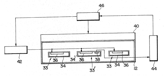
FIG. 3 is a schematic view of the burn-in
: apparatus according to a first embodiment of this
2073916
SEI 92-16
1 invention. The burn-in apparatus according to the
first embodiment comprises the same burn-in test
chamber 12 including a box body and a lid as the above-
described conventional burn-in test chamber (see FIG.
2). In the burn-in test chamber 12, there is provided
a temperature adjusting unit 40 for adjusting an
environmental temperature in the burn-in test chamber
12 by blowing heated air, or heating by
a heater.
In this burn-in test chamber 12, a plurality of
burn-in boards (not shown) are disposed, and a
plurality of semiconductor devices 33, 33' are mounted
on each burn-in board by means of sockets (not shown).
Any suitable socket for setting the semiconductor
device on the burn-in board 10 can be used. FIGs. 4
and 5 show a preferred example of a socket 16 for set
the semiconductor device 33 on the burn-in board 10.
Each socket 16 fixed on the burn-in board comprises a
base 70 and a lid q2 connected to the base 70 openably
2~ by a hinge 74. When a lever 76 attached to the lid 72
is locked with a hook 78 formed on the base 70, the
,
base 70 is closed by the lid 72. In the central
portion of the base 70, there is formed a cross-shaped
concavity 80. A plurality of~terminals 82 are provided
on the bottoms o~ the arm portions of the concavity 80.
207391~
SEI 92-16
1 One ends of the respective terminals 82 are projected
from the underside of the base 70 to be connected to
the wirings (not shown) on the burn-in board 10. A
through-hole 84 is formed in the central portion of the
cross-shaped concavity 80. A heat conducting member 86
is secured by a screw 88 to the central portion o~ the
lid 72. This member 86 comprises a flat panel so on
the side o~ the lid 72 to be opposed to the base 70,
and heat radiation panels 92 formed integrally with the
flat panel 90 and extended through the lid 72.
The semiconductor device 33 has a plurality of
terminals 39 provided on the underside thereof. These
terminals 39 are brought into contact with
corresponding terminals 82 of the socket 16 when the
semiconductor device 33 is mounted in the socket 16.
When the~semiconductor device 33 is placed in a
concavity 80 and the~lid 72 is closed, the flat panel
; ~ 90 of the heat conducting member 86 is brought into
contact with the top surface of ~the semiconductor
; 20 ~ device 33 so that the~heat of the semiconductor device
33 or semiconductor chip 34 can be conducted and
radiated.
All the semiconductor device 33, 33' incIude
semiconductor chips 34 having integrated circuits 36
built in, respectively. In this embodiment, one 33' of
11
207391~
SEI 92-16
1 the semiconductor devices 33, 33' additionally has a
-temperature detection diode 38 as a temperature sensor
formed on the built-in semiconductor chip 34'. This
semiconductor device 33' having the temperature
detection diode 38 is set at a position where a highest
environmental temperature Ta is present in the burn-in
test chamber 12.
:: :
The position where a highest environmental
temperature Ta is established in the burn-in test
chamber 12 is usually an upper location where the
heated air tends to stagnate. Accordingly, it is easy
to find such location on the basis o~ positions and
; shapes of outlet nozzles of the heated air.
In a burn-in test,~ an electric load is separately
applied to the integrated circuits of the respective
semiconductor chips 34, 34' by elec~ric power supplying
means 42, and electric characteristics (especially
changes of a~forward~voltage (threshold~voltage) VF) of
the temperature detection diode 38~of the semiconductor
~; ~ 20 chip 34' are monitored by temperature detecting unit
.,
~ 44, so that a junction temperature Tj of the
~ ` :
semiconductor chip 34' is measured. the measurement of
this junction temperature Tj is conducted in the
following way.
In measuring electric characteristics of the
12
20739~
SEI 92-16
1 temperature detection diode 38, a junction temperature
of the temperature detection diode 38 is measured. The
heat resistance of the semiconductor chip 34' is
sufficiently smaller than heat resistances of its
ambient substancas (air, or molding materials), and the
following relationships are given.
(A junction temperature of the temperature
detection diode 38) ~ (A junction temperature o~ the
integrated circuit 36) = Tj
Hereinafter both junction temperatures are
; represented commonly by Tj.
FIG. 6 shows a perspective view o~ the
semiconductor chip 34' involved in the above-described
embodiment. FIG. 7 is~a graph of an I-V characteristic
of the temperature detectlon diode~38 at a temperature.
As shown in FIG. 6, on the semiconductor chip 34',
:
there are formed the integrated circuit 36, the
temperature detection diode 38, a power supply pad 35
connected to the inte~grated circuit 36 and monitoring
pads 37 conneoted to the anode an~d the cathode of the
temperature detection diode 38. This semiconductor
chip 34' is packaged in a flat package or a leadless
chip-carrier (LCC) as a semiconductor device 33' to be
burn-ln tested. The temperature monitoring for this
semiconductor chip 34' is based on the observation of
:
13
.
20739~ ~
SEI 92-16
l an I-V characteristic of the temperature detection
diode 38. That is, the forward voltage VF of the I-V
characteristic of FIG. 7 changes substantially linearly
with respect to junction temperatures in a range o~
junction temperatures exhibited in a burn-in test of
the semiconductor device. This relationship is
; approximately expressed by the following Formula 1.
F ~ TC Tj + V~0 (1)
V~ : Forward voltage of a temperature
detection diode
TC : Temperature coefficient o~ VF value
Tj : Junction temperature of a semiconductor
device or chip to be tested
VF0 : Constant given for each semiconductor
~device~or chlp to be tested
A current flowing through the;temperature detection
diode 38 whén a forward vol~tag~e VF is applied thereto is
so trivial that the temperature detection diode does
not contribut~ much to increases of a junction
temperature. When the forward voltage~VF is measured
with the integrated circuit 36 unfed, a junction
temperature Tj agrees;with an~envlronmental temperature.
A first temperature measurement technique uses the
above-described property, and the flow chart of this
technique is shown in FIG. 8. First, values of a
14
2~7391~
SEI 92-16
1 forward voltage VF are measured at different
environmental temperatures with the integrated circuit
36 unfed (Step 101). Based on the measured values o~
the forward ~oltage and Formula 1, a value of a
constant VFo of the forward voltages VF, and a value of
a temperature coefficient TC o$ the forward voltages V~
are given (Step 102). Following this preparation, a
burn-in test is started, and during the burn-in test,
temperatures o~ the semiconductor chips 34' are
accurately detected. That is, semiconductor chips 34'
are mounted on the burn-in apparatus, and while the
integrated circuits 36 are in operation with a current
supplied to, values of the forward voltages VF are
measured (Step 103). Values of the junction
temperatures Tj are given based on the value of the
constant VFo~ the value of the temperature coefficient
TC, and measured values of Porward Yoltages VF (Step
104).
Also. the following second junction temperature
measurement technique can give measured values of
precision as high as the first technique.
EIG. 9 shows the flow chart of the second
junction temperature measurement technique. First, a
value of a constant V~0 of~a temperature detection diode
38 formed on the semiconductor chip 34', and an ideal
207391~
SEI 92-16
1 value n thereof are given at the room temperature (Step
201). Here, a forward current IF of the Schottky type
temperature detection diode 38 is given by the
following Formula 2.
IF K SA*T2~xp(- kT )exp( nkT) ........ (2)
S : Schottky junction area
A: Effective Richardson constant
T : Absolute temperature
: k : Boltzmann constant
q : Electron charge
~B: Barrier height
n : Xdeal factor
A forward threshold voltage VF of the temperature
~ detection diode 38 and an ideal factor n thereof can be
: given based on an I-V characteristic of the temperature
detection diode 38. A temperature coefficient TC of
the temperature detection diode 38 is given by the
: following Formula 3.
TC- dTF _ nk (2-in ~ ~ ----- (3)
Variations of a value of the~second term in the
parentheses of Formula 3 are sufflciently:small in the
junction temperature range of burn-in tests, so that
the TC value is almostly proportional to the n value.
: This relation between TC and n was:confirmed by an
experimental result shown in FIG. 16.
16
2~73~1~
SEI 92-16
1 A temperature coefficient TC of the forward
voltage Vp is given by Formula 1 and 2 (Step 202) to
detect an accurate temperature of the semiconductor
chip 34' during a burn-in. That is, semiconductor
chips 34 are mounted on the burn-in apparatus, and
while the integrated circu~its 36 are in operation with
a current suppl1ed to, values of the forward threshold
voltages Vp are measured (Step 203). Then, based on the
value of the constant V~0 given at the room temperature,
the values of the threshold voltages Vp given real time
~; during a burn-in, and a value of the ideal factor n,
junction temperatures Tj of the temperature detection
diodes 38, i.e, surface temperatures of the
semiconductor chips 34', are given real time (Step
204).
Here FIG. 3 is again referred to. The burn-in
apparatus àccording to thls invention includes control
device 46. This control device 46 controls the
, ~
electric power supplying unit 42 based on a monitor
result of the temperature ~detectlng~unit 44 to control
electric power feed amounts to the integrated circuits
36 of all the semiconductor chips 34, 34' in an
allowable range. To this end, the control device 46
stores an allowable range~of the junction temperature T
~ for a burn-in test, and is so programmed that the
;~ 17
2073~1~
SEI 92-16
1 electric power supplying unit 42 is suitably controlled
based on a result of a comparison between the stored
allowable temperature range and a monitor result.
The method for controlling the electric power
supplying unit 42 will be explained in more detail. In
the case that the control device 46 recognizes based on
a monitor result of the temperature detecting unit 44
that a junction temperature Tj of the semiconductor chip
34' of the semiconductor device 33' has exceeded a set
allowable maximum temperature, the electric power
amounts supplied to all the semiconductor chips 34, 34'
are decreased to lower 3unction temperatures Tj of the
respecti~e semiconductor chips 34, 34'. A junction
temperature Tj of the semiconductor cnip 34' with the
temperature detection diode 38 is higher than junction
temperatures Tj of the other semiconductor chips 34,
because the semiconductor chip 34' is located at a
position where an environmental t~emperature is highest.
Accordingly, by lowering j~unction temperatures Tj of all
~ . ~
the semiconductor chips 34, 34' as a whole, the
semiconductor chips 34, 34' do not have junctlon
temperatures above the allowable temperature range.
:
Thus, screening test are prevented from being
reduced to different purposes? and accurate screening
- is enabled.
18
2~73~16
SEI 92-16
1 In the above-description, the temperature
detection diode 38 is provided on one semiconductor
chip 34', but the temperature detection diode 38 may be
provided on each of the semiconductor chips 34, and
that of the semiconductor chip having a highest
junction temperature may be monitored.
~ Also, as a method for lowering junction
;~ temperatures Tj, it is possible that the temperature
adjusting unit 40 ~or adjusting an environmental
temperature Ta is controlled to lower an environmental
temperature Ta as a whole.
FIG. 10 is a schematic VleW 0~ the burn-in
apparatus according to a second embodiment of this
invention. The second~embodiment is the same as the
irst embodiment except that the temperature detection
diode 38 as the temperature sensor is provided on each
of the semiconductor ch1ps~34, and junction
temperatures o~ the respective temperature detection
diodes 38 are measured by the temperature~detecting
unit 44. ~ ~ ~
In this second embodiment, the control device 46
is programmed so as, when~monitored junotion
temperatures Tj contain a Junction temperature outside
an allowable temperature range, to control electric
power supplying unit 42 to adjust an electric power
19
2073~1~
SEI 92-16
feed amount to the semiconductor chip 33 having such
junction temperature is adjusted.
A method for controlling the electric power
supplying unit 46 used in the second embodiment will be
explained in more detail with reference to the ~low
chart of FIG. 11. An allowable junction temperature
range or a suitable test temperature is set by an
operator and is stored in a memory of the control
device 46 (Step 301). When a burn-in test is started,
electric characteristics of the respective temperature
detection diodes 38 are individually monitored by the
temperature detecting unit 44, and junction
temperatures Tj o~ the respective semiconductor chips 34
(Step 302). The actually measured values of the
junction temperatures Tj of the respective semiconductor
chips 34 and the set allowable temperature range are
compared by the control;device 46 ~(Step 303). An
electric power supplied to that of~the semlconductor
chips 34 whose monitored junction temperature is below
the set allowabl~e temperature range is increased (Step
304), and an electric power supplled~to that of the
semiconductor chips whose monitored junction
temperature is below the set allowable temperature is
decreased (Step 305). :For example, in the case a set
allowable temperature range is 145 ~ 155~C, i~ a ~irst
2~7391~
SEI 92-16
1 semiconductor chip has a junction temperature of 140C,
and a second semiconductor chip has a junction
temperature o~ 160~, an electric power to the first
semiconductor chip is increased, and that to the second
semiconductor chip is decreased. It should be noted
that increases and decreases of an electric power is
within an allowable range for a burn-in test. When an
electric power is increased, a heat generation amount
of the associated integrated circuit 38 is increased,
and the junction temperature Tj is raised to the set
allowable temperature range. When an electric power is
decreased, a heat generation amount of the integrated
circuit 38 is decreased, and the junction temperature T
is lowered to the set allowable temperature range.
; Steps 302 ~ 305 are repeated, whereby the junction
temperatures Tj are maintalned within the set allowable
temperature range.
In the case that junction temperatures Tj of a
~ plurality of semiconductor chips 34 are outside an
allowable temperature range as described above, a burn-
:
in test does not have ko be conducted at unnecessarily
high temperatures, because an electrlc power feed
amount is controlled ~or the respective semiconductor
chips. Accordingly, accurate screening is enabled.
It should~be noted that decreases and increases of
21
: 2~739~
SEI 92-16
l an electric power feed amount may be made beyond an
allowable feed amount range in burn-in tests for the
purpose of finding ~ailures which do not depend on
electric power ~eed amounts.
In the second embodiment, the temperature
detection diode 38 is formed on each of the
;~ semiconductor chips 34, but may be ~ormed on at least
two of the semiconductor chips, preferably on that at
a location where an environmental temperature is
~10 lowest, and also on that at~ a location where the
~;~ envlronmental temperature is highest. In this case, it
is necessary that junction temperatures of the
semiconductor chips at other locations are estimated
based on a difference between monitored temperatures of
~; the two semiconductor ch1ps, and based on an estimation
result, an electric power is controlled~for the
respective semlconductor chips. ~ ~
In the case that~the temperature detection diodes
38 are provlded~on~all the semlconductor chips as shown
20~ in FIG. lO, the fol~lowlng method~or~controlllng the
electr1c power supplying unit 42 can be applied.
As shown in the ~flow chart o~ FIG. 12, an
allowable junction temperature range or a suitable test
temperature is set by~an operator and is stored in a
memory of the control device 46 (Step 401). When a
22
20739i~
SEI 92-16
1 test is started, electric characteristics o~ respective
temperature detection diodes 3~ are individually
measured, and junction temperatures Tj of the respective
semiconductor chips 34 are individually monitored (Step
402). A measured value o~ the junction temperature Tj
: of each semiconductor chip 34 is compared with the set
allowable temperature range (Step 403). Those of the
semiconductor chips 34 whose measured junction
: temperatures are below the set allowable temperature
range are continuously fed with an electric power, and
the electric power supply is stopped to those of the
semiconductor chips 34 whose measured junction
temperatures Tj are above the set allowable temperature
range (Step 404). After the electric power supply is
: : .stopped, the monitor of the junction temperatures are
: continued (Step 405). When the junction temperatures T
: ~ ~ have lowered to the set allowable temperature range,
the electric power supply i9 resumed -to the
:
semiconductor chips 34 (Step 406). Thus, the ON/OF~
o~ the electric power supply to those of the
,: ~
semiconductor chips whose junction temperatures have
: ~
risen above the set allowable temperature range is
controlled so that a burn-in test is conducted in a
suitable temperature range. Accordingly, accurate
screening can be conducted. It is preferable that a
23
207391 ~
SEI 9Z-16
1 time of a pause of the electric power supply is omitted
from a time of a screening test, and to this end, it is
preferable that a time ol a pause of the electric power
supply is individually monitored.
As shown in the flow chart of FIG. 13, in the case
that a junction temperature Tj of one of the
semiconductor chips 34 is judged to be above a set
allowable maximum temperature (Step 503), it is
possible that the electric power supply to all the
semiconductor chips 34 are stopped (Step 504). When
such high junction temperature has fallen to the set
suitable test temperature following a pause of the
; ~ electric power supply, the electric power supply to all
the semiconductor chips 34 are resumed (Steps 505,
506). Since Steps 401 and 402 of the flow chart of
FIG. 13 are the same as Steps 401 and 402 of the flow
chart of FIG. 14, their explanation is omitted.
Thus, the electric power supply to all the
semiconductor chips 34 is paused, whereby a burn-in
::
~ 20 test is paused.~ Consequently, a burn-in test lS
-~ prevented from being reduced to dif~erent proposes, and
accurate screening is enabled.
In the case that~the ON/OFF o~ the electric power
supply to all the semiconductors 34 is controlled, it
is not necessary that each of the semiconductor chips
24
2~73~l~
SEI 92-16
1 34 has the temperature detection diode 38. Instead, it
is possible that the temperature detection diode 38 is
formed on the semiconductor chip o~ a semiconductor
device to be set at a location where a high
environmental temperature Ta is expected, and the
semiconductor chip is monitored.
It is also possible that the temperature adjusting
unit 40 is controlled to increase and decrease an
environmental temperature Ta in the burn-in test chamber
; 10 12, whereby junction temperatures o~ the semiconductor
: chips 34 are adjusted.
FIG. 14 is a flow chart o~ such control method.
Similarly with the above-described embodiment, a
suitable temperature range for a burn-in test is set by
; an operator and is stored in a memory o~ the control
device 46 (Step 601). A~ter the test lS started,
: ~ electric characteristics o~ a plurality o~ temperature
detection diodes 38 are measured to monitor junction
temperatures Tj of the respective semiconductor chips 34
(Step 602). The number or ratio o~ those of the
~: : semiconductor chips 34 whose junction temperatures T
are outside the set suitable temperature range is
measured, and the number or ratio o~ those of the
semiconductor chips 34 whose junction temperatures T
fall in the set suitable temperature range when the
2~
2073916
SEI 92-16
1 environmental temperature Ta is changed is simulated
(Step 603).
Then, it is checked whether an ideal environmental
temperature at which the number or ratio of those o~
the semiconductor chips 34 which is within the set
suitable temperature range becomes maximum is higher or
lower than the present environmental temperature (Step
604). Based on a given temperature condition, the
temperature adjusting unit 40 is controlled to raise
1~ the present environmental temperature (Step 605) or
lower the present environmental temperature (Step 806).
Steps 60~ and 606 are repeated to maintain an ideal
condition in which the number o~ those of the
semiconductor chips whose junction temperatures Tj are
in the set suitable temperature range.
FIG. 15 shows the above-described simulation in a
graph. That lS, in FIG. 15, the monitored junction
temperatures Tj~are taken on the horizontal axis, and
the numbers of the semiconductor chips are taken on the
vertical axis. The numbers or ratios of those of the
,.
semiconductar chips whose junction temperatures Tj are
in the set suitable temperature range at three
environmental temperature ranges Tal, Ta2, Ta3 are shown.
Here it is assumed that at the environmental
temperature Tal the ratio is 65%, that at the
Z6
2~7391~
SEI 92-16
1 environmental temperature Ta2 is 85%, and that at the
environmental temperature Ta3 is 60%. In this case,
when the present environmental is Tal, the control is
conducted to raise this environmental temperature, and
when the present environmental temperature is Ta3~ the
control is performed to lower this environmental
temperature.
Thus, a screening test is prevented from being
reduced to a different purpose, and accurate screening
is enabled. Since the environmental temperature Ta f
the interior of the burn-in test chamber 12 varies at
locations in the chamber 12 depending on mounted
; ~ positions of the temperature adjusting unit 40 or
others, some of the semiconductor devices 33 are
surrounded by a too high temperature, and others of the
semiconductor devices 33 are surrounded by a too low
temperature~ In this embodiment, the temperature
adjusting unit 40 is so controlled that a largest
number of the:semiconductors have a suitable junction
temperature. Accordingly, accurate screening can be
conducted.
The junction temperature monitoring does not have
: to be conducted on all:the semiconductor chips, but it
is possible to monltor junction temperatures of only
those of the semiconductor chips at locations where a
27
207~
SEI 92-16
1large environmental temperature di~erence is expected.
The temperature sensors used in this invention are
not limited to temperature detection diodes, such as
Schottky junction diodes, formed on the semiconductor
chips separately from the integrated circuits, and
instaad may use diodes or transistors built in the
integrated circuits. Otherwise, NiCr or WSi metal film
resistors may be formed on the semiconductor chips.
From the invention thus described, it will be
10obvious that the invention may be varied ln many ways.
Such variations are not to be regarded as a departure
from the spirit and scope of the invention, and all
such modi~ications as would be obvious to one skilled
in the art are intended to be included within the scope
of the ~ollowing claims.
:: :
~ 20
,: :
28