Note: Descriptions are shown in the official language in which they were submitted.
2083 1 22
OPTICAL DEVICES VVITH ELECTRON-BEAM
EVAPORATED MULTILAYER MIRROR
Field of the Invention
The invention conf e,-l.s Vertical Cavity Surface F.mitting Lasers.
5 Back~round of the Invention
Stacks of ~l~ern~ting high and low rcirl~ c~ index layers serve as
miIrors in Vertical Cavity Surface F.mitfing Lasers, hereinafter referred to as
VCSELs. The task is to find suitable materials for the high and low index layerswhich maximize a ratio of the high index refractive order to the low index refractive
10 order, and which could he ~eposil~d in a Ill~mer comratihle with the semirQn~ ctor
device processing
A VCSEL is attractive as a device in which the lasing cavity is
perpen-lir.ll~r to the top surface of a laser chip, which is small and which may be
produced by planar technology. This can lead to a pl~ ;ng future in high densit
15 laser arrays, high data tr~nsmic~ion in optical co,...,~"ir~tion ~y~t~ ms, ultra high
parallel processing in optical co~ nir~tit~n ~y~ ls, as well as supplying a route
for data tr~n~mi~sion be lw~n electronic chips. Fullll~lllole, dhe circular-like nature
of their beams allows one to efficiendy couple dhe laser light into circular optical
fibers.
In dhe VCSEL dhe light output is in dhe film growth direction which is
usually parallel to dhe direction of dhe injection current. Due to dhis feature, the
mirror through which dhe emi~siQn takes place and dhe electrical contact physically
occupy the same side of the laser structure, i.e. either the top or the bottom of the
device. The mirror is located a~pl~imately in the center of dle surface while the
25 electrode is located peripherally of dhe mirror. An example of a surface emitting
laser widh a coplanar lllill~,./electrode arrangement in which a gold layer with a
thirl~ness of a few tendhs of a micr~ ,t~,r acts as the mirror dlrough which laser-
emi~sion takes place, may be found in articles by H. Soda et al., enfitlç~l
"GaInAsP/InP Surface F.mitting Injection Lasers," J~ nrsc Journal f Applied
30 Physics, Vol. 18, No. 12, 1979, pp. 2329-2230; and by H. Soda et al. entitled"GaInAsP/InP Surface F.mit~ing Injection Lasers widh Short Cavity T Pngth," IEEEJournal f Quantum Electronics, Vol. QE-l9, No. 6, June 1983, pp. 1035-1041.
However, S. Kinoshita pointed out that such mirrors lead to low quantum efficienr-y
primarily due to absorption of lasing emission by dhe gold mirror and suggested the
35 use of a stack of pairs of dielectric layers as the top mirror, one layer of each pair
~'
-2- 2083 1 22
having a higher index of refracdon than the other layer of the pair. See an ardcle by
Susumu Kinosl~ et al. endtled "GaAlAs/GaAs Surface F.mining Laser with High
Relleu,li~c, TiO2/SiO2 Muldlayer Bragg E2PflP~tor," Jar~nese Journal f Applied
Physics, Vol. 26, No. 3, March 1987, pp. 410-415; L. M. Zinkiewicz et al., "High5 Power Verdcal-Cavity Surface-Fmitting AlGaAs/GaAs Diode Lasers," Appl. Phys.
Letters, Vol. 54, No. 20, 15 May 1989, pp. 1959-1961; and KPni~hi Iga, "Recent
Advances of Surface F.mitting Semi~Q~ ct~r Lasers," Ol,loele~l,oi1ics-Devices and
Technolo.~ies, Vol. 3, No. 2, Decernher 1988, pp. 131-142.
TiO 2 and ZrO 2 quarter-wave ( 4~ ) dielectric layers have been typically
10 paired with SiO2 quarter-wave layers. The number of pairs is selected to obtain a
IllaXilllUIll pelrO....~n~e reflecdvity. However, the mirror structures of alternadng
TiO2 (or ZrO2) and SiO2 quarter-wave layers have not yielded expected
pelrollllance, in terms of reflecdvity. Theoretically, the opdcal ~lrO. .n~nce of a
stacked mirror structure should a~r~ach 100 percent. Unrol~ui1aLely, plesel,lly
15 obtainable pelro~ ance falls within a broad range of from 90 to 99 percent. The
problem resides, primarily, with the high index layer m~t~n~l~ This shorLfall is,
most likely, due to the diffirulty in obtaining suffi~içntly high quality TiO2 (or
ZrO2) layers on a reproducible basis. Electron-beam deposidon of co~ ting~, such as
TiO2 (or ZrO2), l~Uil~S a~lition of oxygen in the d~silion process to get the
20 proper stoiciometry for a desired refracdve index. ~ liti~n of oxygen is needed to
avoid formadon of unwanted, oxygen-defi~ient phases, such as Ti, TiO, Ti 2 3,
Ti3 Os, which occur due to an oxygen shortage. This ~ui~ nt makes it difflcult
to reproducibly form the TiO2 layer.
Several single crystal sçmicontluctors with high index of refracdon,
25 such as Al ,~ Ga 1 _ ~ As or GaInP, which possess the desired plu~l lies whenepitaxially del)o~;t~l may be used in place of TiO 2 or ZrO 2 layers; however, the
epitaxial growth of these mqt~i~ uil~S le.ll~latures of - 600-800C along with
sophisdcated, e~ 1si~,e growth app~lus. These m~tçri~l~ are poorly suited for
deposition in a device post-p~cessing wherein ~"lperatures above 300-350C are to
30 be avoided. Th~"~fole, there is sdll a need for high stability, high ~,Çol,ll~ce
mirrors for use in VCSELs with high quality coadngs which are easily reproducible
at con~litio~ co...~ ible with the device pl~)cess;ng and which could be also
produced in a simplified Illalmer utili7ing planar te~hnology.
-
3 2083 1 22
Summary of the Invention
This invention embodies a VCSEL with a top mirror co~ lising at
least one pair of quallel~ave layer, each pair collsis~ g of a low index of refraction
layer and a high index of refraction layer, the high index of refraction layer being a
5 semiconductor chosen from GaP and ZnS and the low index of refraction layer being
chosen form borosilicate glass (BSG), CaF2, MgF2 and NaF. Especially useful in
vertical cavity surface emitting lasers are mirrors formed by a stack of a plurality of
pairs of GaP/BSG or ZnS/CdF2. Such mirrors are produced by e-beam deposition in
the absence of oxygen and have a high reflectivity chara~-tçri~ti~s required for an
10 efficient operation of the laser. The GaP/BSG or ZnS/CaF2 mirror structures
represent a considerable improvement over previous designs for VCSELs in terms of
ultimate reflectivity, low loss, and post growth processing co.l-~ ,ility.
In accordallce with one aspect of the invention there is provided an
optical device colll~lisillg a semiconductor m~ri~l selected from the group co~
15 of III-V and II-VI semiconductors, collllJlising a lasing cavity and top and bottom
metal electrodes for applying electric field to the lasing cavity, said lasing cavity
comprises a bottom mirror, a bottom collfll~illg region, an active region, a top collfll~ g
region and a top mirror, said top mirror comprising a plurality of pairs of qual~cl~vàve
layers, each pair of layers col~ ing of a low index layer and a high index layer20 arranged in an allç...~ g sequçnre beginning with the low index layer, wherein said
high index layer is a semiconductor selected from the group consisting of GaP and
ZnS, and said low index layer is of a m~tçri~l chosen from the group of materials
selected from borosilicate glass (BSG), CaF2, MgF2 and NaF.
In accordance with another aspect of the invention there is provided a
25 method of fabricating a laser device colllllisillg a semiconductor material selected from
the group consisting of III-V and II-VI semiconductors, said device COlll~ illg a lasing
cavity and top and bottom metal electrodes for providing electric field to the læing
cavity, said lasing cavity inrlurling a bottom mirror, a bottom confining region, an active
region, a top collflllillg region and a top mirror, said top mirror colll~lishlg a plurality
30 of pairs of quarterwave layers, each pair of layers col.~ g of a low index ofrefraction layer and a high index of refraction layer, which COlll~liSCS dc~osiLing said
quarterwave layers of the top mirror by electron-beam deposition from corresponding
source materials in a vacuum en~dloll,llcll~ with ~"l.~l~"li~l absence of oxygen, said high
2083 1 22
-3a-
index of refraction layer is selected from the group consi~li,lg of GaP and ZnS and the
low index of refraction layer is selected from the group co~ g of borosilicate glass
(BSG), CaF2, MgF2 and NaF.
Brief Des~ tion of the Dl~w;~ .c
FIG. 1 is a cross-sectional view of a structure of a VCSE laser;
FIG. 2 is a chart representing a Reflectivity versus Wavelength curve
"l~asuled for a mirror with 6 pairs of ZnS/CaF2;
FIG. 3 is a chart representing a Reflectivity versus Wavelength curve
measured for a mirror with 3 pairs of GaP/borosilicate glass; and
FIG. 4 is a chart l~lese,l~ g the Illc~uled optical data for a 40rJm
thick GaP film on borosilicate glass in terms of tr~nsmission and reflection.
Detailed Description
The applicants have discovered that such semiconductor materials as
GaP and ZnS represent an excellent choice for the high index layers in mirrors for use
in VCSELs especially if combined with such low index dielectric layers as CaF2, MgF2,
NaF and borosilicate glass (BSG). The index of refraction of GaP is 3.45, of ZnS is
2.35, and of BSG, CaF2, MgF2, NaF the index of refraction is 1.46,1.42,1 .389, and
1.317,re~ecliv~1y. GaP and ZnS are compound semiconductors which can be
deposited by electron-beam (E-beam) evaporation in the form of amorphous layers, at
2 0 relatively low ~ulJ~llale tell,~eldlules and without the need for oxygen supply during
the deposition. E-beam evaporation, a relatively in~el~ive technique, produces no
.signifi~nt damage to the semiconductor surface and permits in situ lll~nilolillg of the
layer thickness. E-beam ~val~oldlion is well-known in the art and, thus, does not need
any further elaboration. For an example of a suitable ~paldlUS for a two layer
2 5 deposition by e-beam technique see the article by Susumu Kino~shit~ et al., supra, or
U.S. Patent 3,984,581 issued to Herman R. Dobler et al.
20831 22
on October 5, 1976.
E-beam d~ ;ol- of GaP and ZnS in absence of oxygen leads to
deposits which are in an ~~ ,hous rather than crystalline state if the substratete~ tule is ~ inl~in~d during deposition at a ~lll~la~ within a range of from
S room ~ e~ G to 250C. These ~e..~ res are conlr~tihle with present
co.. ~.-ly used device pl~)cesses, such as oxide d~,posilion or m~t~lli7~tion~
~lthough the deposited layers are not single crystal, absorption losses are low for
wavelengths within a range of from 0.5 to 1.6 ~m, preferably from 0.5 to 1.1 ~m
and most preferably from 0.85 to 0.88 ~lm (emission ~. a~,eleAgth of bulk GaAs).10 Good quality GaP and ZnS layers are obtained in~ependently of the substrate
material making such mirror structures as GaP/BSG or ZnS/CaF2 readily
reproducible. In contrast to the use of TiO2 or nnmodifiecl ZrO2, in combinationwith SiO 2 layers, control of film stoi~hiom~try using GaP or ZnS as a high index
coating is not a problem, and leads to an eYcell~nt reproducibility.
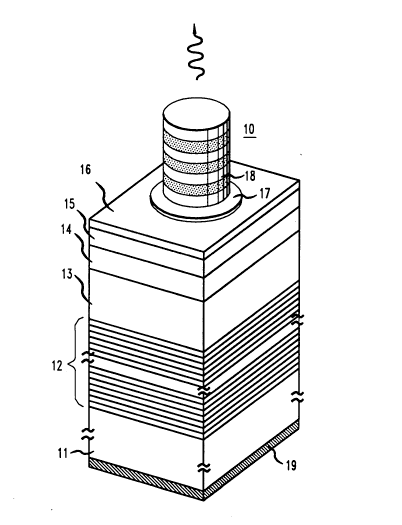
FIG. 1 is a schf .. ~;c .~ ,se .-~l;on of a VCSEL according to this
invention, denomin~te~l generally as 10. For reasons of clarity elements of the
VCSEL are not drawn to scale. VCSEL 10 co,-~.ises a substrate 11; a quarter-wavestack of a plurality of pairs of semiconduc~or layers forming a bottom mirror, 12, one
layer of each pair having a refractive index difr~lcnt from the .~r.a~ re index of
20 another layer of the pair, a first co~rl~ing layer, 13; an active layer, 14; a second
co~lr~ g layer, 15; a highly-doped contact layer, 16; a metal ring which acts as a
non-alloyed ohmic top electrode, 17, of the device; a second quarter-wave stack of a
plurality of pairs of layers forming a top mirror, 18, one layer of each pair having a
refractive index dirr~ t from the refractive index of another layer of the pair, and a
25 bottom electr~de, 19, in contact with the bottom surface of substrate 11. While not
shown, ~ddition~l confining and buffer layers may be included into the laser
structure. The number of pairs of layers is ~billa,ily shown as being 3; however,
this number may be anyone within a range of from 2 to 20.
Construction of VCSEL 10, in acco~lce with the invention, may be
30 described as being generally as follows:
Substrate 11 is an n+ - type III-V or II-VI æmicontluctor~ such as GaAs,
GaInAs, InP, GaInP, GaInPAs, AlAs, AlGaAs, AlGaInAs, AlInP, AlInPAs,
AlGaInPAs and other related group III-V or II-VI co-.-~owld æmiconductors.
Typically, the thi~ness of the substrate ranges from 100 to 500 llm and the doping
35 concentration of the substrate ranges from 1 x 10¹⁷ to 1 x 10l9 cm~3. In someapplic~fion~, such as opto-electronic integrated cil~;uill~, substrate 11 may be first
2083 1 22
- 5 -
grown on a master substrate of silicon, which is in co.-~.--on to a numbe. of devices
grown on the master substrate.
Quarter-wave stack 12 is compose~ of a plurality of pairs (or periods) of
layers of n + - type se-miron~ ctor, such as GaAs, GaInAs, InP, GaInP, GaInAsP,
S AlAs, AlGaAs, AlInP, AlGaInP, AlGaInAsP, the semiron~lctl~r layers forming a
bottom multilayer distributed Bragg reflector (DBR) mi~or with a number of pairstypically ranging from 10 to 40. One sem -on~l~]ctor layer in each pair has a higher
index of refraction than the other semicQn~luctor layer of the pair. The thickness of
each semi~Qn~ ctor layer in the pair equals 4~, wl~elein A is the optical ~a~elength
10 of the laser device and n is the refractive index of the layer. For example, for a
device with an active region lasing at ~ ~ 0.87 ~m, such as a GaAs-based laser, a
quarter-wave stack of pairs of such semicond~ctors as GaAs and AlAs with
~Ll~li. indices of 3.64 and 2.97, le~ ly, will consist of 60 nm thick GaAs
layer and 73 nm thick AlAs layer while a stack of Alo.os GaO.gs As and AlAs will15 consist of pairs of layers 62 nm and 73 nm thick each, l~s~cli~rely.
First co~.fining layer 13 and second conrnil-g layer 15 are provided to
confine acdve region 14 and to adjust the length (L) of an optical cavity (that is, the
thirl~ness of the active region). The optical cavity length should be 2L=N-~,
wL~leill N is an integer and ~ is an ope-a~-ng optical wavelength of the laser.
20 Typically, the thirl~nçss of each conrnh~g layer ranges from 0 to 3 llm. To obtain
constructive in~lrel~ince, the thir~ness of the conr..-il-g layers should be a multiple
of 4~ . In the plefell~d embo~limrnt the co n r ,.i ng regions are of Al ,~ Ga I _ " As,
with x ranging &om 0.1 to 0.4.
Active region 14 is a region in which electrons (-) and holes (+)
25 recoll,bille providing, under proper stimlll~tiQn a lasing emission~ In the pl~rell~,d
e.llbo~li...r-nt, the active region is a lightly doped (1 x 10l6 - Sx 10l7 cm-3) layer of
GaAs with a thir~nrss within a range &om 0.1 to 1 ~lm. The single layer may be aho...o~;~ neous semicQn(l~lctor or a single or multiple quantum well (QW) structure,
composed of a n~l~w.,l gap semirQ~ lctor confined by a wider gap semiconductor.
30 ~ltern~tively, the single layer forming the active region may be replaced by a
s~lperl~ttire structure which is a multiquantum well structure with very thin barriers.
Highly doped contact layer 16 is provided in thin~ness of from 0.01 to
0.1 llm to f~cilit~tr establishing a non-alloyed ohmic contact between conrl-ling
layer 15 and ring electrode 17. Typically, the doping concentration in the contact
35 layerrangesfrom 1x10l9 to lxl020cm-3.
2083 1 22
Elec~ de 17 is a non-alloyed ohmic cont~ct Electrode 17 is of a metal
selected from such metal colllpo~ite,s as AuBe and AuZn de,po ,ited in a thirl~nPss of
from S to 400 nm thick in the form of an ~nnnlll~ with from 1.0 to 50 ~m outer
moter and from 0.5-25 ~m inner ~ ~ter. Such contacts are del)os;t~ cl by
S e~a~,~ on at t~,lJ~.~IUI~S ranging from 20C to 500C, preferably from 20C to250C. Higher te,l~ ul~s could result in undesi~ble alloying of the metal into the
semiconductor. ~d~lition~lly~ a thin layer of such metal as Pt may be position~
.~n contact layer 16 and the metal comros;te.
Top mirror 18 is a multilayer Bragg ,~ ol inclufling from 2 to 20
10 pairs of high index and low index layers stacked one upon another in a cohlmn~r
f~hion In one p,~,ftl,~d el~bofl;...~ nt the high index layers are GaP and the low
index layers are borosilir~tr glass (BSG) such as Vycor~. In another pl~re.l~d
embo~li.... ......R,n~, the high index layers are ZnS layers and the low index layers are CaF2
layers.
Metal elc~ de 19 from 1 to 10 ~m thick is formed on the bottom
surface of substrate 11 to provide for current flow perpendicularly through the active
region to cause lasing emi~sion The laser may be mounted with electrode 19 in
contact wit,h a heat-sink plate, e.g. of copper or some other heat-conductive material
which does not con~ e the mat,erials of the laser.
Sem:^onductor layers 12 through 16 can be grown upon substrate 11 by
such known method$ as metal organic vapor phase epitaxy (MOVPE), also known as
metal organic chrmir~l vapor deposition (MOCVD), or by Molecular Beam Epitaxy
(MBE) or by hydride vapor phase epitaxy (VPE). In the p,~fell~d emb(Ylimrnt, theVCSEL struct,ures are grown by the MBE t,echnology in a Varian Gen II MBE
system on heavily doped GaAs substrates 11. After layers 12 t,hrough 16 are grown,
the partially formed slluclu,e is transferred to a separate high vacuum chamber
where a metal layer is deposited by electron beam tvap~ ion on exposed portions
of contact layer 16 as a non-alloyed ohmic contact in a thir~ness sllmrient to
provide desired electric~l conductivity. Electrode 17 may be deposited through a30 photolithographically formed mask or through a shadow mask blocking off areas on
which depo~ilion of the metal electrode is to be eYrl-lded, such as the centrally
located area of the contact layer. Following the top electrode deposilion step, the top
mirror stack is deposited in absence of oxygen through a shadow mask by electronbeam e~,alion either in the same or in another chamber. Bottom electrode layer
35 19, e.g., of In, may then be formed on the bottom surface of substrate 11. Finally,
the bottom side of the la~ser may be ~ untcd via the In electrode or by means of a
2083 1 2Z
co~ adhesive, such as epoxy, on a copper slab which serves as a heat sink inCO~1J11 on to other devices.
The flow of elc~llvns from top ele~ vde 17 may be le~l,icli~ely directed
to the active layer through a small contrally located window (not shown) defined in
S CO~ l~ning layer 15. This central area preferably cO~ subst~nti~lly to the
central opening in the annular electlvde. It maybe produced con~,eniel lly by ion-
implanting the ~lil,hel~l area of co~ ing layer 15 with ions which do not affect the
con~ ctivity type of the material in which they are implanted. Proton ions, such as
H+ ,O+ or He+ are implanted typically in concentrations ranging from 1 x 10l8 to10 5 x 10 19 per cm3 . They are implanted into the peripheral area of confining layer 15
prior to the deposllion of contact layer 16, thus defining a window for the centrally
restricted flow of electrons to active layer 14.
In the exemplary plefel.~d embod~llent, the VCSEL is an Al " Ga 1 _ ,~ As
laser structure, with x ranging from 0 to 1.0, compri~ing in an ~cen-ling se~uence 1
15 to 2 llm thick In electrode 19, about 500~m thick (001)-ori~nte~ heavily doped
(2x 10l8 cm~3 ) n+ -GaAs substrate 11, bottom mirror 12 con~i~ting of a quarter-wave stack of 30 pairs of n+-type (Sx 10l7 - Sx 10l8 cm~3) semicon~luctor layersforming multilayer distributed Bragg reflector (DBR) mirror, each pair of the stack
con~i~tin~ of a 73 nm thick layer of n+ - AlAs and 62 nm thick layer of
20 Alo 05 GaO 95 As. The reflectivity s~~ ll of this DBR structure, as measured with
a Perkin-Elmer ~ ~mh~lfl 9 UV/VISINIR Sp~;ll~hololl~t.,~, showed a broad high
reflectivity band cente.~d at -0.8711m with a reflectivity > 99 percent. The bottom
mirror is followed by first co~ nt layer 13 of n+ -Al0.20Gao.80 As
(SxlOl7cm~3) about 3 ~lm thick, lightly doped (SxlOl6cm~3) acdve layer 14 of
25 p~ -GaAs about 0.6 ~m thick, and second confin~ment layer 15 of
p+-Al0.30GaO.70As(SxlOl6cm~3)aboutO.Sllmthick. Aheavilydoped(5
xlOl9cm~3) contact layer 16 of p+ -AlO.lOGao.goAs, about 0.06 ~m thick, is
deposit~d on c~ -g layer 15 for ohmic contact purpose. Electrode layer 17 of
AuBe about 200 nm thick is formed, through a suitable mask, on top of contact layer
30 16 under co~iitiQns leading to a non-alloyed ohmic contact. Electrode layer 17 is in
the form of an ~nnlllus with from 1.0 to 50.0 ~m, preferably 5 to 25 ~m, outer
m~ter and about from 0.5 to 20 ~m, preferably 2 to 20 ~m, inner ~ .,.. t~-r.
A plurality of alternating layers of GaP and BSG or ZnS and CaF2,
forming top mirror 18 are then d~,positcd by e-beam evaporation. These layers are
35 deposited through a mask so as to form a cylindrical column of alternating layers.
The deposition begins with a BSG (or CaF2) layer followed by the deposition of
~083 1 22
- 8 -
GaP (or ZnS, lc,i.~li~ely) layer and repetiti~n of the deposit se~uel ce until adesired nulllber, e.g., 20, of BSG-GaP (or CaP2 - ZnS) pairs are deposil~3 The
stack is then preferably capped off with another BSG (or CaF2) layer.
The source mqteriql for dcpo~ilion of GaP layers was pol~l ~lline
5 GaP and for deposition of BSG layers was fused BSG. Similarly, the source
material for del)o~;lion of ZnS layers was crystalline ZnS and for deposition of CaF2
layers was crystalline CaF2. After bolllba~ nl of the source materials was
initiqted, an about 150 nm thick BSG (about 153 nm thick CaF2) layer was
pe ..~ ,d to be ~lepos~ A on an a~ ce.-l central region of contact layer 16 and in
10 pardally overlapping reladon on e,-posed pordons of contact 17 while the deposidon
of GaP was avoided by means of a shutter. Theleart4r about 64 nm thick GaP (about
93 nm thick ZnS) layer was d~,posite~ while the d~posilion of the BSG layer was
inle~ pled. This procedure sequence was le~at~,d undl a desired nu.ll~r of pairs(periods) of BSG and GaP (or CaF2 and ZnS, respecdvely) layers was d~posit~d.
15 During the deposition, the vacuum was kept within a range of from 1 x 10⁻⁴ to 1 x
10-7 Torr. Outer ~liqm~t~or of the stack was larger than the inner fliqm~ter of
ele~:l,ode 17 so as to overlap the cle~ )de by from 0.2 to 5 ~m. During the
deposition the substrates were held at t~lll~latures of 125C - 250C. These
~ pelalul~s are co...~ ;ble with device processes, such as oxide d~posilion or
20 metqlli7vtion, co.-....ollly used as a post semicond~lctor growth processin~ These
t4lll~lalul~,s are also con~lcive to the formqtion of amorphous films of GaP andZnS in absence of an oxygen al---o,l,h~ . E-beam e~apolation of allel,laling GaPand BSG layers or ZnS and CaF2 layers in accol~lce with this invendon produces
desired index of refracdon without introducdon of oxygen into the evaporadon
25 chqrnber. Thus, there was no need to introduce oxygen into the chamber, and none
was introd~lce~l
FIG. 2 shows a l~inu;~ivi~ versus wavelength curve measured for a six
pair ZnS/CaF2 quarter-wave mirror on Si. A reflectivity of >97% is obt~Lih~ed at a
~a.elength range of from 0.80 to 0.90 ~Lm.
FIG. 3 shows a reflecdvity versus wavelength curve measured for a 3
pair GaP/BSG quarter-wave mirror on Si. A reflectivity of >97% is obtained at a
wavelength of about 0.87 ~lm. Ad~litir~nqlly~ a ll~ul~d opdcal data in terms of
trn~mi~sion and reflection is shown in FIG. 4 for a 400A GaP film deposited at asubstrate ~-ll~lature of 250C. Over the wavelength range of 0.7 - 1.1 ~lm no
35 measurable absorpdon takes place in the GaP film.