Note: Descriptions are shown in the official language in which they were submitted.
2~5~5~
SEI 93--3
TITLE OF THE INYENTION
Semiconductor Device
BACKGROUND OF THE INVENTION
Field of the Invention
_
The present invention relates to a semiconductor device
used in Si-LSI, GaAs-LSI and liquid crystal display(LCD).
Related Background Art
In packaging a flip chip,-all bumps formed on a
semiconductor chip are connected to pads of a substrate. To
this end, a technique to keep parallelism between the
semiconductor chip and the substrate is very important. A
prior art technique to keep parallelism between the
sem.iconductor chip and the substrate includes a method
which uses an optical probe. In this method, a probe light
is directed to the semiconductor chip and the substrate, a
relative inclination between the semiconductor chip and the
substrate is measured based on a reflec$ed light, and the
parallelism therebetween is adjusted based on the
measurement.
Since a recent semiconductor chip is highly integrated,
th~re are many fine ruggedness on the surface of the
semiconductor chip. ThUs, even if the probe light is
directed to the semiconductor chip by using the optical
probe, the light is scattered by the fine ruggedness on the
surface of the semiconductor chip so that it is difficult to
measure the relative inclination between the substrate and
S~5~
SEI 93-3
1 the semiconductor chip.
Further, there are a number of fine ruggedness on a
surface of a packaging substrate which is basically a
ceramic substrate such as Al203 or AlN, or a porous metal
such as CuW. As ~ result, even if the probe light is
directed to the packaging substrate by using the optical
probe, the light is scattered by the fine ruggedness on the
surface of the packaging substrate so that it is difficult
to measure the inclination of the packaging substrate.
SUMMARY OF THE INVENTION
It is an object of the present invention to provide a
semiconductor device comprising substrate having a light
reflecting area selectively formed on a required region for
a packaging surface of a semiconductor chip.
In the present invention, when the parallelism of the
packaging substrate is adjusted by using measurement means,
a light is irradiated to the light reflection area formed in
the packaging substrate, and the inclination of the
packaging substrate is de~ermined based on the reflection
angle. Since the light reflec~ion area is formed to have a
flat surface, an error includsd in the reflection angle of
light from the light reflection area is very small.
Accordingly, the precision in adjusting the parallelism of
the packaging substrate is improved.
The present invention will become more fully understood
from the detailed description given hereinbelow and the
' ~
~39~;55~L
SEI 93-3
accompanying drawings which are given by way of
illustration only, and thus are not to be considered as
limiting the present invention.
Fur~her scope of applicability of the present invention
will become apparent from the detailed description given
hereinafter. However, it should be understood that the
detailed description and specific examples, while
indicating preferred embodiments of the invention, are
given by way of illustration-only, since various changes and
modifications within the spirit and scope of the invention
will become apparent to those skilled in the art form this
detailed description.
BRIEF DESCRIPTION OF THE DRAWINGS
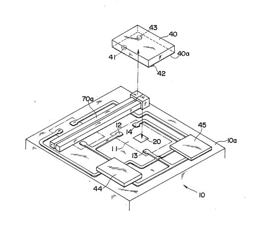
Fig. 1 shows a perspective vi w of an external view of a
packaging apparatus in an embodiment,
Fig. 2 shows a sectional view of a structure of a flat
area 20, which is formed on the packaging substrate shows
Fig. 1,
Fig. 3 shows a manufacturing process of the flat area 20,
which is formed on the packaging substra~e shows Fig. 1,
Fig. 4 shows a manufacturing process of the flat area 20,
which is formed on the packaging substrate shows Fig. 1,
Fig. 5 shows a manufacturing process of the flat area 20,
which is formed on the packaging substrate shows Fig. 1,
Fig. 6 shows a perspective view of a.structure of a
packaging plana of a semiconductor chip,
G551
SEI 93-3
Fig. 7 shows a perspective view for illustrating
measurement of parallelism between the semiconductor chip
and the packaging substrate,
Fig. 8 shows a perspective view of an external view of
the packaging substrate and the semiconductor chip having
a plurality of flat areas,
Fig. 9 shows a plan view for illustrating measurement of
parallelism between the sQmiconductor chip and the
packaging substrate,
Fig. 10 shows top views of arrangements of the flat area
on the pacXaging area of the packaging substrate,
Fig. 11 shows top views of arrangements of the flat area
on the packaging area of the packaging substrate,
Fig. 12 shows top views of arrangements of the flat area
on the packaging area of the packaging substrate,
Fig. 13 shows top views of arrangements of the flat area
on the packaging area of the packaging substrate,
Fig. 14 shows top views of arrangements of the flat area
on the packaging area of the packaging substrate,
Fig. 15 shows top views of arrangements of the flat area
on the semiconductor chip,
Fig. 16 shows top views of arrangements of the flat area
on the semiconductor chip,
Fig. 17 shows top views of arrangements of the flat area
on the semiconductor chip,
Fig~ 18 shows top views of arrangements of the flat area
~96~5~
SEI 93-3
on the semiconductor chip,
Fig. 19 shows top views of arrangements of the flat area
on the semiconductor chip,
Fig. 20 shows a plan view of the packaging apparatus, and
Fig. 21 shows a perspective view for illustrating a
principle of measuremen~ of an optical probe.
DETAILED DESCRIPTION OF THE PREFERRED EMBODIMENTS
One embodiment of the present invention is now described
with reference to the accompanying drawings. Fig. 1 shows
a perspective view of an external view of a packaging
apparatus in one embodiment. A plurality of semiconductor
chips 40, 44 and 45 may be mounted on an upper surface lOa
o~ a packaging substrate 10 and metal wirings are formed on
the upper surface lOa to interconnect the semiconductor
chips 40, 44 and 45. A plurality of bumps 41 - 43 is formed
in a packaging plane 40a of the semiconductor chip 4Q. A
plurality of pads 12 - 14 which are to face the bumps 41 - 43
are formed ln a packaging area 11 on the upper surface lOa
on which the semiconductor chip 40 is to be packaged, and a
flat area 20 having an area of IO - 200 ~m2 is provided at a
center of the packaging area 11. The bumps 41 - 43 formed
on the semiconductor chip 40 are connected to the pads 12 -
; 14 and the semiconductor chip 40 is packaged on the
packaging substrate 10. A ceramic substrate such as Al203
or AlN, or a porous metal such as CuW is used for the
packaging substra~e 10.
~)9~
SEI 93-3
As the scale of the packaging substrate 10 recently
increases, it has become difficult to make the entire upper
surface 10a flat. Particularly when the ceramic is used for
the packaging suhstrate 10, it is more difficult because of
warp and twist inherent to the ceramic. As a result, in the
case that the upper surface 10a of the packaging substrate
10 has a large area, a relative inclination between a
packaging portion on the upper surface 10a and a packaging
surface 40a of the semiconductor chip 40 differs depending
on which part the semiconductor chip 40 is packaged on.
Thus, it is not sufficient to adjust the parallelism
between the entire upper surface 10a of the packaging
substrate 10 and the packaging surface 40a of the
semiconductor chip 40, and it is further necessary to adjust
the parallelism bet~een a portion of the upper sur~ace 10a
of the pac~aging substrate 10 and the packaging surface 40a
of the semiconductor chip ~0.
One o~ methods for adjusting the parallelism between the
upper surface 10a of the packaging substrate 10 and the
packaging surface 40a of the semiconductor chip 40 uses an
optical probe 70a. In this adjustment method, ~he optical
probe 70a i~ arranged between the ~ackaging substrate 10 and
the semiconductor chip 40 and two probe lights are emittsd
to the packaging substrate 10 and the semiconductor chip 40.
By measuriny the reflectio~ angles of the probe lights at
the pa~kaging substrate 10 and the semiconductor chip 40,
': . . ' - :
i5~L
SEI 93-3
1 a relative inclination between the upper surface lOa of the
packaging substrate 10 and the packaging plane 40a of the
semiconductor chip 40 is detected. Based on the detection,
a relative parallelism between the upper surface lOa of the
packaging substrate 10 and the packaging plane 40a of the
semiconductor chip 40 is adjusted. In the present
embodiment, sinr~ the flat area 20 for reflecting the probe
light is provided in the upper surface lOa of the packaging
substrate 10/ the reflection angle of the probe light at the
packaging substrate 10 is accura e.
As shown in Fig. 2, the flat area 20 has a three-layer
structure having an insulation film 101, a metal layer lOZ
and an insulation film 103 sequentially laminated on the
packaging substrate 10. The insulating film 101 is applied
a~ an underlying layer of the metal layer 102 which is used
as a reflection mirror surface for the probe light, by the
following reason. The upper surface lOa of the packaging
substrate 10 has more ruggedness than the surface of the
semiconductor chip 40 which uses a mirror-~inished wafer
such as GaAs or Si as a base material. For example, an Al203
ceramic substrate having a surface thereof not polished has
ruggedness in the order of R~ - 10 ym. A substrate which
uses CuW as a base material has ruggedness in the order of
R~ = 5 ym even after the surface is polished. Accordingly,
when the metal layer 102 is deposited directly on the
packaging substrate 10, similar unevenness appears on the
~0~6~
SEI 93-3
1 surface o~ the metal layer 102 so that the probe light may
not be reflected exactly. In the present embodiment, the
insulation film 101 of a sufficient thickness is applied to
the packaging substrate 10 to make the surface of the
insulation film 101 flat, and the metal layer 102 is
deposited on the insulation film 101 so ~hat the metal layer
102 having a flat surface is formed.
- A manufacturing proc~ss of the flat area 20 is shown in
sectional views of ~igs. 3 to 5. First, an insulative
material is applied to the packaging suhstrate 10 to a
thickness of 5 ~m or more by a spin coat method, for
exampla, to form the insulation film 101 (see Fig. 3). As
the insulative material, PI (polyimide), BCB
(benzocyclobetene) or SOG (spin-on glass) may be used.
Alternatively, those materials, may be sequentially applied
to form a multi-layer insulation film 101. Then, a resist
pattern haring an opening in an area in which the flat area
20 is to be formed is formed on the insulation film 101, and
the metal layer 102 such as ~u, Cu or Al is
sputter-deposited by using the resist pattern as a mask Ssee
Fig. 4). After the resist pattern 104 has been removed, an
insulation film material is deposited by a plasma cvn
method, for examplet to form the insulation film 103 (see
Fig. 5). The insulatioD film material may be SiN
(refractive index n is approximately 1.9), SiON (n is
approximately 1.85) or SiO2 (n is approximately 1.4). The
2~9~
SEI 93-3
1 insulation film 103 is preferably deposited to a thickness
which meet~ a relationship of A/2xm = nxd, where A is a
wavelength of the probe light, m is an integer and d is a
film thickness. If the film thickness meets the above
relationship, a reflection factor of the probe light which
is reflected by the metal layer 102 of the flat area 20 is
ma~imum and the reduction of the light intensity of the
probe light by the insulation film 103 is minimized.
Fig. 6 shows a perspective view of the semiconductor chip
40 having a flat area 50 in the packaging plane 40a as the
packaging substrate 10 has. A metal wiring 44 is formed on
the packaging plane 40a of the semiconductor chip 40 as
shown in Fig. 6, and bumps 41 - 43 are form2d at a plurality
of areas of the metal wiring 44. A flat area 50 having an
area of 10 - 200 ~m2 is provided at a center of the packaging
plane 40a of the semiconductor chip 40. The flat area 50 is
used when the parallelism between the semiconductor chip 40
and the packaging substrate 10 is measured. As shown in
Fig. 7, the probe ligh~ is reflected with an accurate angle
by directing the probe ligh~ from ~he optical probe 70a to
the flat area 50 of the semiconductor chip 40.
The flat area 50 may be formed by laminating an
insulation film on the metal layer. The insulation film may
be SiN (refractive index n is approximately 1.9), SiON (n is
approximately 1.85) or SiO~ (n is approximately 1.4). The
insulation film is preferably laminated to a thickness
20~6~5~
SEI 93-3
1 which meets a relationship of A/2xm - nxd where A is a
wavelength of the probe light, m is an integer and d is a
film thickness. When the film thickness meets the above
relationship, the reflection factor of the probe light
reflected by the metal layer o~ the ~lat area 50 is maximum
and the reduction of the light intensity of the probe light
by the insulation film is minimized. Further, since the
flat area 50 is formed at the center of the packaging plane
40a of the semiconductor chip 40, the parallelism between
the semiconductor chip 40 and the packaging substrate 10 can
be accurately adjusted even if distortion or warp is
included in the periphery of the packaging plane 40a.
The flat area 20 and the flat area 50 are preferably
arranged in such a positional relation that the areas at
least partially overlap when the semiconductor chip 40 is
packaged on the packaging substxate 10. The sizes of those
areas need not be equal and one area may be covered by the
other area.
Since the flat areas 20 and 50 are formed to have flat
surfaces, the intensities of the lights reflected by the
flat areas 20 and 50 are larger than those of the lights
reflected by other areas than the flat areas 20 and 50. As
a result, whether ~he probe light is reflected by the flat
area 20 or 50 can be determined by measuring the intensity
of the reflected light. Accordingly, where the flat area 20
and the flat area 50 are arranged to partially overlap,
i5S~
SEI 93-3
coarse positioning of the packaging substrate 10 and the
semiconductor chip 40 may be done by moving the packaging
substrate 10 and the semiconductor chip 40 parallelly to the
packaging plane 40a, so that intensities of the lights
reflected on the packaging substrate 10 and the
semiconductor chip 40 are increased.
Referring to Figs. 8 and 9, the adjustment of the
parallelism between the packaging substrate 10 and the
semiconductor chip 40 by using a plurality of flat areas is
explained. Fig. 8 shows a perspective view of an external
view of ths packaginy substrate 10 and the semiconductor
chip 40 having a plurality of flat areas. A plurality of
bumps 41 - 43 and flat areas 51 - 53 are formed on the
packaging plane 40a of the semiconductor chip 40. A
packaging area 11 is which the semiconductor chip 40 is to
be packaged is provided in the upper surface lOa of the
packaging substrate 10, and pads 12 - 14 which are to ~ace
the bumps 41 - 43 and flat areas 21 - 23 which are to face,
the flat areas 51 - 53 are provided in the packaging area
11. The flat areas 21 - 23 and the 1a~ areas 51 - 53 are
arranged in such a positional relation that the respective
area~ at least partially overlap when the semiconductor
chip 40 is packaged on the packaging substrate 10.
Accordingly, the sizes o~ the respec~ive areas need not be
equal and one area may be covered by other area. The size
of the respective areas i5 10 - 200 Am2.
f;~51
SEI 93-3
As shown in Fig. 9, the flat areas 21 - 23 and 51 - 53 are
used as reflection planes of the probe light from the
optical probe 70a irradiated to measure the parallelism
between the packaging substrate 10 and the semiconductor
chip 40. The relative inclination of the packaging
substrate 10 and the semiconductor chip 40 can be accurately
detected based on the reflection angle by reflecting the
probe light by the flat areas 21 - 23 and 51 - 53.
Arrangements of the flat areas on the packaging area 11
of the packaging substrate 10 are shown in Figs. 10 - 14.
In Fig. 10, a pair of flat areas 24 - 25 are providsd
symmetrically abou~ a center of gravity lla of the packaging
area 11 of the packaging substrate 10. The parallelism may
be accurately adjusted even if distortion or warp is
in~luded in the entire uppsr surface lOa, by measuring the
parallelism between the packaging substrate 10 and the
semiconductor chip 4U at two points by using the flat areas
24 and 25.
In Fig. 11, two pairs of flat areas 26 and 27 and flat
areas 28 and 29 are provid~d symmetrically about a center of
gravity lla of the packaging area 11 of the packaging
substrate 10. In the present embodiment, the parallelism
between the packaging substrate 10 and the semiconductor
chip 40 is measured at the four flat areas 26 ~ 29 so that
the parallelism can be more accurately adjusted than the
previous embodiment. In the present embodiment, since the
12
,
;55il
SEI 93-3
flat areas 26 - 29 are arranged such that straight lines
connecting the pairs o~ flat areas are substantially normal
to each other, the parallelism can be accurately adjusted
even if distortion or warp is included in the entire upper
surface lOa.
In Fig. 12, a cross-shaped flat area 30 is provided at
the center of the packaging are~ 11 of the packaging
substrate 10. A plurality of measurement points are
selected from ends 30a - 30d of the flat area 30 to measure
to parallelism between the packaging substrate 10 and the
semiconductor chip 40. Thus, the parallelism can be
accurately adjusted even if distortion or warp is includ~d
- in the entire upper surface lOa.
In Fig. 13, a band-like flat area 31 is provided at a
periphe~y of the packaging area 11 of the packaging
substrate 10. A plurality of measurement points on the fla~
area 31 are selected to measure the parallelism between the
packaging substrate 10 and tha semiconductor chip 40 so that
the parallelism can be accurately adjusted.
Fig. 1~ shows a modification of the embodiment of Fig.
13. A plurality of flat areas 32 - 35 are provided at the
- periphery of the packaging area 11 of packaging substrate
10. The parallelism can be accurately adjusted, as it is in
the embodiment of Fig. 13, by using the flat areas 32 - 3S.
Arrangements of the fla~ areas on ~he semiconductor
chips 40 are shown in Figs. 15 - 19. In Fig. 15, a pair o~
5~
SEI 93-3
flat areas 54 and 55 are provided symmetrically about a
center of gravity 40b of the packaging plane 40a of the
semiconductor chip 40. By measuring the parallelism
between the semiconductor chip 40 and the packaging
substrate 10 at two points by using the flat areas 54 and
55, the parallelism can be accurately adjusted even if
distortion or warp is included in the entire packaging plane
40a.
In Fig. 16, two pairs of flat areas 56 and 57 and flat
areas 58 and 59 are provided symmetrically about the center
of gravity 40b of the packaging plane 40a of the
semiconductor chip 40. In the present embodiment, since the
parallelism between the semiconductor chip 40 and the
packaging substrate ~0 is measured at the four flat areas 56
- 59, the parallelism can be more accurately adjusted than
the previous embodiment. Further, since the flat areas 56
- 59 in the present embodiment are arranged such that
straight lines connecting the paired flat areas are
substantially normal to each other, the parallelism can be
accurately adjusted even if distortion or warp is included
in the entire packagîng plane lOa.
In Fig. 17, a cross-shaped flat area 60 is provided at a
: center of the packaging plane 40a of the semiconductor chip
40. A plurality of measurement points are selected from
ends 60a - 60d of the flat area 60 to measure the
parallelism between the semiconductor chip 40 and the
14
.
;5~
SEI 93-3
1 packaging substrate 10 so ~hat the parallelism can be
accurately adjusted even if distortion or warp is included
in the entire packaging plane 40a.
In Fig. 18, a band-like flat area 61 is provided at a
pariphery of the packaging plane 40a of the semiconductor
chip 40. A plurality of measurement points on the flat area
61 are selected to measure the parallelism between the
semiconductor chip 40 and the packaging substrate 10 so that
the parallelism can be accurately adjusted.
Fig. 19 shows a modification of the ~mbodiment of Fig.
18. A plurality of flat areas 62 - 6S are provided at a
periphery of the packaging plane 40a of the semiconductor
chip 40. Like in the embodiment of Fig. 18, the parallelism
can be accurately adjusted.
A packaging apparatus for packaging the semiconductor
chip 40 to the packaging substrate 10 is now explained with
reference to Fig. 20. The packaging apparatus comprises a
semiconductor chip mount unit 81 having the semiconductor
chip 40 mounted on a bottom surface thereof by vacuum
sucking and a substrate mount unit 82 having the packaging
substrate 10 mounted on an upper surface thereof by vacuum
sucking. The semiconductor chip mount unit 81 is fixed to
a top of a frame 83 and the substrate mount unit 82 is fi~ed
to a bottom of the frame 83. A parallelism measurement
de~ice 70 for measuring the parallelism between the
packaging substrate 10 and the semiconductor chip 40 is
~9~
SEI 93-3
provided between the semiconductor chip mount unit 81 and
the substrate mount unit 82.
The parallelism measurement device 70 comprises an
optical probe 70a for irradiating a probe light to the
packaging substrate 10 and the semiconductor chip 40, a
measurement unit 70b for measuring reflection angles of the
probe light reflected by the packaging substrate 10 and the
semiconductor chip 40, and a support member 70c for
supporting the optical probe 70a and the measurement unit
70b.
The semiconductor chip moun~ unit 81 comprises a sucking
block 811 for sucking the semiconductor chip 40, a swingable
stage 812 having the sucking block 811 fixed thereto, and a
horizontally movable staye 813 movable in a horizontal
two-dimensional plane and having the swingable stage 812
fixed thereto. Actuators 81a and 81b for adjusting a
direction parallel to the upper surface of the
semiconductor chip 40 are provided on two planes which are
perpendicular to the side of the horizontally movable stage
813, and actuators 81c and 81d for adjusting the inclination
of ths semiconductor chip 40 are provided on two planes
which are perpendicular to the side of the swingable stage
812.
The substrate mount uni~ 82 comprises a sucking block B21
for sucking the packaging substrate 10, a vertically
movable bonding mechanism 822 having the sucking block 821
16
5~
SEI 93-3
1 fixed thereto, a swingable stage 823 having the bonding
mechanism 822 fixed thereto, and a horizontally movabl~
stage 824 movable in a horizontal two-dimensional plane and
having the swingable stage 823 fixed thereto. Actuators 82a
and 82b for adjusting a direction parallel to the upper
surface of the packaging substrate 10 are pro~ided on two
planes which are perpendicular t the side of the
horizontally movable stage 824, and actuators 8~c and 82d
for adjusting the inclination of the packaging substrate 10
are provided on two planes which are perpendicular to the
side of the swingable stage 823.
The packaging apparatus further comprises a controller
84 for adjusting the parallelism between the packaging
substrate 10 and the semiconductor chip 40. The controller
84 receives measurement data from the optical probe 70a and
issues necessary commands to the actuators 81a - 81d in
accordance with the data.
A principle of measurement of the optical probe 70a is
now explained with reference to Fig. 21. Incident lights A
and Bl parallelly directed from a light source pass through
a light guide 70aI, are reflected by reflection mirrors 70a2
and 70a3, and are dlrected to the lower surface of the
semiconductor chip 40 and the upper surface of the packaging
substrate 10. The illumination lights A2 and B2 are
reflected by the lower surface of the semiconductor chip 40
and the upper surface of the packaging substrate 10 and exit
17
.
5~
SEI 93-3
1 through the reflection mirrors 70a2 and 70a3. The exit
positions of the exit lights A3 and B3 are measured by a
semiconductor position detector to determine a relative
angular shift between the lower surface of the
semiconductor chip 40 and the upper sur~ace of the packaging
- substrate 10.
Turning back to Fig. 20, a packaging method by using the
packaging apparatus is now explained. The semiconductor
chip 40 is sucked by the sucking block 811 of the
semiconductor chip mount unit 81 and the packaging
substrate 10 is sucked by the sucking block 821 of the
substrate mount unit 82. The parallelism between the
packaging substrate 10 and the semiconductor chip 40 is
measured by using the parallelism measurement device 70.
The probe light directed to the packaging substrate 10 is
accurately refl~cted by the flat area 20, and the probe
light directed to the semiconductor chip is accurately
reflected by the flat area 50. By measuring those reflected
lights, the inrlination between the packaging substrate 10
20 ` and the semiconductor chip 40 can be accurately detected.
The mea~urement da~a of the parallelism measurement
device 70 is sent to the controller 84 which determines the
parallelism between the packaging substrate 10 and the
semiconductor chip 40. If the controller determines that
the angle adjustment of the packaging substrate 10 is
necessary, commands are issued ~o the actuators 8~c and 82d
18
.
,' , ' , , - ,
X O~ 35 1
SEI 93-3
of the pac~aging substrate mount unit 82 to conduct the
necessary angle adjustment. If the controller 84
determines that the angle adjustment of the semiconductor
chip 40 is necessary, commands are issued to the actuators
81c and 81d of the semiconductor chip mount unit 81 to
conduct the necessary angle adjustment.
When the angle adjustment is completed, the parallelism
measurement unit 70 is retracted. Then, the subs~rate mount
unit 82 is lifted up and the semiconductor chip 40 is
packa~ed on the packaging substrate 10. Since sufficient
parallelism between the packaging substrate 10 and the
semiconductor chip 40 has been attained in the previous
angle adjustment process, all bumps on the semiconductor
chips 40 can be connected to the pads on the packaging
substrate 10. Accordingly, a high packaging yield is
assured.
The reflection o the probe light is more accurate if the
surface lOa of ~he pac~aging substrate 10 or the packaging
plane 40a of the semiconductor chip 40 is polished. From
the invention thus described, it will be obvious that the
invention may be varied in many ways. Such variations are
not to be regarded as a departure from the spirit and scope
of khe in~ention, and all ~uch modifications as would be
obvious to one skilled in the art are intended to be
included within the scope of the following claims.
19