Language selection

Search

Patent 2105039 Summary

Third-party information liability

Some of the information on this Web page has been provided by external sources. The Government of Canada is not responsible for the accuracy, reliability or currency of the information supplied by external sources. Users wishing to rely upon this information should consult directly with the source of the information. Content provided by external sources is not subject to official languages, privacy and accessibility requirements.

Claims and Abstract availability

Any discrepancies in the text and image of the Claims and Abstract are due to differing posting times. Text of the Claims and Abstract are posted:

  • At the time the application is open to public inspection;
  • At the time of issue of the patent (grant).
(12) Patent: (11) CA 2105039
(54) English Title: SEMICONDUCTOR DEVICE AND WAFER STRUCTURE HAVING A PLANAR BURIED INTERCONNECT BY WAFER BONDING
(54) French Title: DISPOSITIF A SEMICONDUCTEUR ET STRUCTURE DE PLAQUETTE A INTERCONNEXION PLANAR ENFOUIE REALISEE PAR SOUDAGE
Status: Deemed expired
Bibliographic Data
(51) International Patent Classification (IPC):
  • H01L 23/522 (2006.01)
  • H01L 21/44 (2006.01)
  • H01L 21/441 (2006.01)
  • H01L 21/48 (2006.01)
  • H01L 21/74 (2006.01)
  • H01L 21/762 (2006.01)
  • H01L 21/98 (2006.01)
(72) Inventors :
  • BUTI, TAQI NASSER (United States of America)
  • HSU, LOUIS LU-CHEN (United States of America)
  • JOSHI, RAJIV VASANT (United States of America)
  • SHEPARD, JOSEPH FRANCIS (United States of America)
(73) Owners :
  • INTERNATIONAL BUSINESS MACHINES CORPORATION (United States of America)
(71) Applicants :
(74) Agent: SAUNDERS, RAYMOND H.
(74) Associate agent:
(45) Issued: 1996-10-29
(22) Filed Date: 1993-08-27
(41) Open to Public Inspection: 1994-05-07
Examination requested: 1993-08-27
Availability of licence: Yes
(25) Language of filing: English

Patent Cooperation Treaty (PCT): No

(30) Application Priority Data:
Application No. Country/Territory Date
07/973,131 United States of America 1992-11-06

Abstracts

English Abstract


A wafer structure suitable for the formation of
semiconductor devices thereon and having a buried
interconnect structure for interconnection of desired
ones of the semiconductor devices according to a
predetermined interconnection pattern and a method of
making the same is disclosed. The wafer structure
comprises a primary substrate having a first thickness
appropriate for the formation of the desired
semiconductor devices. The primary substrate further
comprises a) conductive interconnection pads of a second
thickness formed on a bottom surface of the primary
substrate according to the predetermined interconnection
pattern, b) first isolation pads of a third thickness
formed on the bottom surface of the primary substrate
between the conductive interconnection pads, and c)
interconnection pad caps of a fourth thickness formed
upon the surface of the interconnection pads opposite
from the primary substrate, wherein the interconnection
pad caps comprise a material suitable for wafer bonding,
and further wherein the total thickness of the second
thickness and the fourth thickness equals the third
thickness. The structure further comprises a secondary
substrate having an oxide layer thereon bonded to the
interconnection pad caps and the first isolation pads of
the primary wafer.


Claims

Note: Claims are shown in the official language in which they were submitted.


- 11 -
The embodiments of the invention in which an exclusive
property or privilege is claimed are defined as follows:

1. A method of manufacturing a wafer structure suitable
for the formation of semiconductor devices thereon and
having a buried interconnect structure for
interconnection of desired ones of the semiconductor
devices according to a predetermined interconnection
pattern, said method comprising the steps of:
a) providing a primary substrate;
b) forming first isolation pads on a top surface of
the primary substrate according to the predetermined
interconnection pattern;
c) forming conductive interconnection pads on the
top surface of the primary substrate between the first
isolation pads;
d) forming interconnection pad caps upon the
interconnection pads, the top of the interconnection pads
being flush with the top of the first isolation pads, the
interconnection pad caps further being of a material
suitable for wafer bonding;
e) providing a secondary substrate having an oxide
layer on a surface thereof; and
f) bonding the oxide layer of the secondary
substrate to the interconnection pad caps and the first
isolation pads of the primary substrate.

2. The method of claim 1, wherein:
step c) comprises depositing a conductive material on
the primary substrate between said isolation pads and
recessing the conductive material below the top of the
first isolation pads.

3. The method of claim 2, further wherein depositing the
conductive material comprises depositing a refractory
metal silicide.

- 12 -

4. The method of claim 3, still further wherein depositing the conductive
material comprises depositing refractory metal silicon rich tungsten silicide.

5. The method of claim 1, wherein:
step d) comprises depositing a polysilicon layer on top of the first isolation
pads and the conductive interconnection pads and planarizing the polysilicon layer
to be flush with the top of the first isolation pads.

6. The method of claim 5, further wherein depositing the polysilicon layer
comprises depositing N+ polysilicon.

7. The method of claim 1, wherein:
step c) comprises depositing a refractory metal silicide on the primary
substrate between said isolation pads and recessing the refractory metal silicide
below the top of the first isolation pads; and
step d) comprises depositing a polysilicon layer on top of the first isolation
pads and the refractory metal silicide and planarizing the polysilicon layer to be
flush with the top of the first isolation pads.

8. The method of claim 7, further wherein:
depositing the conductive material comprises depositing a refractory metal
silicide, and
depositing the polysilicon layer comprises depositing N+ polysilicon.

9. The method of claim 8, still further wherein depositing the conductive
material comprises depositing refractory metal silicon rich tungsten silicide.

10. The method of claim 1, further comprising the steps of:
g) reducing the thickness of the primary substrate to a thickness
appropriate for the formation of the desired semiconductor devices;


- 13 -
h) forming second isolation pads in the primary
substrate according to the predetermined interconnection
pattern; and
i) forming semiconductor devices in the primary
substrate between corresponding second isolation pads
according to the predetermined interconnection pattern,
wherein the conductive interconnection pads provide
a planar interconnect between desired ones of the
semiconductor devices.

11. The method of claim 10, wherein:
step c) comprises depositing a conductive material
on the primary substrate between said isolation pads and
recessing the conductive material below the top of the
first isolation pads.

12. The method of claim 11, further wherein depositing
the conductive material comprises depositing a refractory
metal silicide.

13. The method of claim 12, still further wherein
depositing the conductive material comprises depositing
refractory metal silicon rich tungsten silicide.

14. The method of claim 10, wherein:
step d) comprises depositing a polysilicon layer on
top of the first isolation pads and the conductive
interconnection pads and planarizing the polysilicon
layer to be flush with the top of the first isolation
pads.

15. The method of claim 14, further wherein depositing
the polysilicon layer comprises depositing N+
polysilicon.

16. The method of claim 10, wherein:
step c) comprises depositing a conductive material
on the primary substrate between said isolation pads and
recessing the conductive material below the top of the
first isolation pads; and

- 14 -
step d) comprises depositing a polysilicon layer on
top of the first isolation pads and the refractory metal
silicide and planarizing the polysilicon layer to be
flush with the top of the first isolation pads.

17. The method of claim 16, further wherein:
depositing the conductive material comprises
depositing a refractory metal silicide, and
depositing the polysilicon layer comprises
depositing N+ polysilicon.

18. The method of claim 17, still further wherein
depositing the conductive material comprises depositing
refractory metal silicon rich tungsten silicide.

19. The method of claim 10, wherein step i) further
comprises 1) exposing desired conductive interconnection
pads and 2) forming desired gates in addition to forming
desired connections between a gate, source, or drain by
way of the exposed interconnection pads, all in the same
step, according to the particular semiconductor devices
being formed and prior to any source/drain implants.

20. A method of manufacturing a wafer structure suitable
for the formation of semiconductor devices thereon and
having a buried interconnect structure for
interconnection of desired ones of the semiconductor
devices according to a predetermined interconnection
pattern, said method comprising the steps of:
a) providing a primary substrate;
b) forming conductive interconnection pads on the
top surface of the primary substrate according to the
predetermined interconnection pattern;
c) forming interconnection pad caps upon the
interconnection pads, the interconnection pad caps being
of a material suitable for wafer bonding;
d) forming first isolation pads on a top surface of
the primary substrate between the conductive
interconnection pads, the top of the first isolation pads
being flush with the top of the interconnection pad caps

- 15 -
e) providing a secondary substrate having an oxide,
layer on a surface thereof; and
f) bonding the oxide layer of the secondary
substrate to the interconnection pad caps and the first
isolation pads of the primary substrate.

21. The method of claim 20, wherein step b) comprises
forming refractory metal silicide interconnection pads.

22. The method of claim 21, further wherein step b)
comprises forming refractory metal silicon rich tungsten
silicide interconnection pads.

23. The method of claim 20, wherein step c) comprises
forming polysilicon interconnection pad caps.

24. The method of claim 23, further wherein step c)
comprises forming N+ polysilicon interconnection pad
caps.

25. The method of claim 20, wherein:
of step b) comprises forming refractory metal
silicide interconnection pads; and
step c) comprises forming polysilicon
interconnection pad caps.

26. The method of claim 25, further wherein step b)
comprises forming refractory metal silicon rich tungsten
silicide interconnection pads.

27. The method of claim 25, further wherein step c)
comprises forming N+ polysilicon interconnection pad
caps.

28. The method of claim 20, further comprising the steps
of:
g) reducing the thickness of the primary substrate
to a thickness appropriate for the formation of the
desired semiconductor devices;

- 16 -
h) forming second isolation pads in said primary
substrate according to the predetermined interconnection
pattern; and
i) forming semiconductor devices in the primary
substrate between corresponding second isolation pads
according to the predetermined interconnection pattern,
wherein the conductive interconnection pads provide
a planar interconnect between desired ones of the
semiconductor devices.

29. The method of claim 28, wherein step b) comprises
forming refractory metal silicide interconnection pads.

30. The method of claim 29, still further wherein step
b) comprises forming refractory metal silicon rich
tungsten silicide interconnection pads.

31. The method of claim 28, wherein step c) comprises
forming polysilicon interconnection pad caps.

32. The method of claim 31, further wherein step c)
comprises forming N+ polysilicon interconnection pad
caps.

33. The method of claim 28, wherein:
step b) comprises forming refractory metal silicide
interconnection pads; and
step c) comprises forming polysilicon
interconnection pad caps.

34. The method of claim 33, further wherein step b)
comprises forming refractory metal silicon rich tungsten
silicide interconnection pads.


35. The method of claim 33, further wherein step c)
comprises forming N+ polysilicon interconnection pad
caps .

- 17 -
36. The method of claim 28, wherein step i) further
comprises 1) exposing desired conductive interconnection
pads and 2) forming desired gates in addition to forming
desired connections between a gate, source, or drain by
way of the exposed interconnection pads, all in the same
step, according to the particular semiconductor devices
being formed and prior to any source/drain implants.

37. A method of manufacturing a wafer structure suitable
for the formation of semiconductor devices thereon and
having a buried interconnect structure for
interconnection of desired ones of the semiconductor
devices according to a predetermined interconnection
pattern, said method comprising the steps of:
a) providing a primary substrate;
b) forming conductive interconnection pads on a top
surface of said primary substrate according to the
predetermined interconnection pattern;
c) depositing a blanket layer of isolation material
onto the top surface of the primary wafer and the
conductive interconnection pads;
d) planarizing the blanket insulation material to
form first isolation pads between the interconnection
pads and to form isolation caps on top of the
interconnection pads, the top of the first isolation pads
being flush with the top of the isolation caps;
e) providing a secondary substrate having an oxide
layer on a surface thereof; and
f) bonding the oxide layer of the secondary
substrate to the first isolation pads and the isolation
caps of the primary substrate.

38. The method of claim 37, wherein step b) comprises
forming refractory metal silicide conductive
interconnection pads.

39. The method of claim 38, further wherein step b)
comprises forming refractory metal silicon rich tungsten
silicide interconnection pads.


- 18 -
40. The method of claim 37, further comprising the steps of:
g) reducing the thickness of said primary substrate to a thickness
appropriate for the formation of the desired semiconductor devices;
h) forming second isolation pads in said primary substrate according to the
predetermined interconnection pattern; and
i) forming semiconductor devices in the primary substrate between
corresponding second isolation pads according to the predetermined
interconnection pattern, wherein the conductive interconnection pads provide a
planar interconnect between desired ones of the semiconductor devices.

41. The method of claim 40, wherein step b) comprises forming refractory metal
silicide conductive interconnection pads.

42. The method of claim 41, further wherein step b) comprises forming
refractory metal silicon rich tungsten silicide interconnection pads.

43. The method of claim 40, wherein step i) further comprises 1) exposing
desired conductive interconnection pads and 2) forming desired gates in additionto forming desired connections between a gate, source, or drain by way of the
exposed interconnection pads, all in the same step, according to the particular
semiconductor devices being formed and prior to any source/drain implants.

44. a wafer structure suitable for the formation of semiconductor devices
thereon and having a buried local planar interconnect structure for interconnection
of desired semiconductor devices according to an interconnection pattern, said
structure comprising:
a) a primary substrate having a first thickness;
b) conductive interconnection pads of a second thickness formed on a
bottom surface of said primary substrate according to the interconnection pattern,
wherein said conductive interconnection pads comprise refractory metal silicide,said refractory metal silicide comprising silicon rich tungsten silicide;
c) first isolation pads of a third thickness formed on the bottom surface of
said primary substrate between said conductive interconnection pads;

- 19 -

d) interconnection pad caps of a fourth thickness formed upon the surface
of said interconnection pads opposite from said primary substrate, wherein the
total thickness of the second thickness and the fourth thickness equals the third
thickness;
e) a secondary substrate wafer bonded to said interconnection pad caps and
said first isolation pads;
f) second isolation pads formed in the primary substrate according to the
interconnection pattern; and
g) semiconductor devices formed in the primary substrate between
corresponding second isolation pads according to the interconnection pattern,
whereby said conductive material provides a local planar interconnect between
desired semiconductor devices.

45. The wafer structure of claim 44, wherein said interconnection pad caps
comprise polysilicon.

46. The wafer structure of claim 44, wherein said interconnection pad caps
comprise oxide.

Description

Note: Descriptions are shown in the official language in which they were submitted.


FI9-92-041 2 10 5 0 3 9

SEMICONDUCTOR DEVICE AND WAFER STRUCTURE
HAVING A PLANAR BURIED INTERCONNECT
BY WAFER BONDING

BACKGROUND OF THE INVENTION

1. Field of the Invention
This invention genera]]y relates to semiconductor
devices on a wafer structure and, more particularly, to
interconnection of the semiconductor devices on the wafer
structure.

. Discussion of the Related Art
By using a local interconnect technique, a 25%
reduction in CMOS SRAM cel] size has been demonstrated as
discussed in 0. Kudoh, et a]., "A new full CMOS SRAM cell
structure," IEDM 1984, pp. ~7-70, while a 64 Mb MOS DRAM
with a 0.4 ~m design ru]e has been reported as disclosed
in M. Sakao, et al., "A c:apacitor-over-bit-line cell with
a hemispherical-grain storage node for 64Mb DRAM," IEDM
1991, pp. 655-658. However, from past experience, there
are many challenges presented when implementing such
local interconnect techniques.
For instance, it is especially difficult to provide
local interconnects when devices are densely packed or
include rough topography. Some examples include: (1)
poor etch selectivity bet;ween the interconnect material
and the active device materia], such as source/drain
areas of an FET, can cause severe etch damage to the
devices when overetch is applied in order to eliminate
unwanted conductive sidewalls; (2) the overall wiring
resistance is not satisfactory because a thin
interconnect is used in order to gain better control on
patterning and also because the effective wiring length
is longer than intended due to the existing topography,
(3) local wiring aggravates the existing topography, and
(4) finally, further sca]ing is limited by ground rules,
e.g., the minimum allowab]e distance between a local
interconnect and a polysilicon gate.

FI9-92-041 2105039

In U.S. 5,010,386, an insulat,or separated vertical
CMOS structure is disclosed. Transistor device layers
are built above and below a buried oxide layer.
Subsequently, CMOS inverters are formed by trench etching
through a transistor stack and connecting desired
transistors. A disadvantage of the '386 structure is
that the forming of a desired structure requires numerous
process steps including exposure of the lower devices to
additional high temperature processing. Additionally,
the positioning and accuracy of an interconnection
between devices is subject to the tolerances of a trench
fill material.
In U.S. 4,829,018, a wafer bonded epitaxial
multilevel integrated circu;t is disclosed. Circuit
devices in the epitaxial layers are interconnected by
forming conductive vias hetween the epitaxial layers.
Such interconnect,ions are non-planar and require complex
lithography steps. This is undesirable since it is not
well suited for manufacturability.
It would thus be desirable to provide an
interconnect str~lcture which results in no damage to
device areas and no added topography which also
eliminates sidewall formation, while providing the
desired interconnections. It would further be desirable
to provide a simp]ified method of interconnecting desired
devices on a substrate.

SUMMAR'Y OF TEIE INVENTTON
It is an object of the invention to overcome the
problems in the art discussed above.

It is an object of the invention to provide an
interconnection method which maintains device area
integrity and eliminates conductive interconnection
sidewall formation.
Still another object of the present invention is to
provide improved packing density.
According to the present invention, a method of
manufacturing a wafer structure suitable for the
formation of semiconductor devices thereon and having a

FI9-92-041 2105039

buried interconnect structure for interconnection of
desired ones of the semiconduc-tor devices according to a
predetermined interconnection pattern comprises the steps
of:
a) providing a primary substrate;
b) forming first isolation pads on a top surface of
the primary substrate accordin.g to the predetermined
interconnection pattern;
c) forming conductive interconnection pads on the
top surface of the primary substrate between the first
isolation pads;
d) forming interc:onllectioll pad caps upon the
interconnection pads, the top of the interconnection pads
being flush with the top of -t;he i.rst isolation pads, the
interconnection pad caps furt}~el being of a material
suitable for wafer bonding;
e) providing a secondary substrate having an oxide
layer on a surface thereof; and
f) bonding. the oxide layer of the secondary
substrate to the interconnection pad caps and the first
isolation pads of the primary substrate.
In addition, accordinc~ to the present invention, a
wafer structure suitable for the formation of
semiconductor devices thereon and having a buried
interconnect structure for interconnection of desired
ones of the semiconc3.uctor devices according to a
predetermined interconnection pattern comprises a primary
substrate having a first th.i.cklles~. appropriate for the
formation of the desirecl sem3colldllctor devices. The
primary substrate further comprises a) conductive
interconnection pads of a second thickness formed on a
bottom surface of the primary suhs-trate according to the
predetermined interconnection pattern, b~ first isolation
pads of a third thickness formed oll the bottom surface of
the primary substrate between the conductive
interconnection pads, and c) interconnection pad caps of
a .fourth thickness formed upon the surface of the
interconnection pads opposit.e from the primary substrate,
wherein the interconnection pad c:aps comprise a material
suitable for wafer bonding, and fllrther wherein the total

~- FI9-92-041 4
2105039
thickness of the second thickness and the fourth
thickness equals the third thickness. The structure
further comprises a secondary substrate having an oxide
layer thereon bonded to the interconnection pad caps and
the first isolation pads of the primary wafer.

BRIEF DESCRIPTION OF T~E ~RAWINGS
The foregoing and other teachings of the present
invention will become more apparent upon a detailed
description of the best mode for carrying out the
invention as rendered below. In the description to
follow, reference will be macle to the accompanying
drawings, in which:
Fig. 1 ta)-(h) show the b~lrled layer interconnect
according to a preferred embodiment of the present
invention at various stacles in the manufacture thereof.
Fig. 2 shows a via connection to the buried layer
interconnect according to a preferred embodiment of the
present invention.
Fig. 3 shows a top view of a semiconductor wafer
structure having a buried layer interconnect according to
the invention.
Fig. 4 shows a top view of a semiconductor wafer
structure havinq an interconnecl- structure according to
the prior art.

DETAILED DESCRIPTION OF TF~ PR~F~RRED EMBODIMENTS
The preferred embodiment of l-l)e present invention is
best understood by referring to Figs. l(a)-(h) of the
drawings, like numerals beinq used for like and
corresponding parts of the various drawings.
According to the present invention, Fig. l(a)
illustrates a cross-sectional view, depicting an initial
processing step for fabricatinq a semiconductor wafer
structure 10 suitable for the formation of semiconductor
devices with interconnections according to a
predetermined interconnect;ion pattern. A primary wafer
or substrate 20 of a first conductlvity type is provided,
the wafer 20, for example, comprising a p-type silicon
substrate. Upon a top surface of primary wafer 20, an

~ FI9-92-041 5
- 210aO39
isolation layer i.s formed and patterned by RIE (Reactive
Ion Etching) etch of the isolation layer and stops at the
primary wafer 20 to provide :isolation pads 22, the
isolation pads 22 def.ini.ng isolation windows 23 ~or
interconnection regions) therebetween. The isolation
windows 23 are patternecl ~ccordil1g to a predetermined
interconnection pattern, as will be further understood in
the description to fol.]ow. Preferably, the isolation
layer comprises a layer of therma~. oxide grown upon the
top surface of primary wafer 2~, the oxide layer being
patterned by RIE etch of the oxide and stop at the
p-silicon substrate to form the first isolation pads 22.
A layer of conductive materia] ~4 is thereafter blanket
deposited over the top surace of primary wafer 20 and
isolation pads 22, fillil~g the above-mentioned isolation
windows 23. The conductive material 24 is then
planarized, for example, by chemi.ca]-mechanical polishing
to leave the conductive material 24 inside the isolation
windows 23 only. The conductive material 24 is then
recess etched below the top .surace of isolation pads 22
(Fig. l(a)). Chemical-mecl).anica1 polishing is well known
in the art and therefore l~Ot discussed herein.
Conductive material 24 can comprise refractory metal
silicide, preferably, a si.licon-rich tungsten silicide
(~Six). A refractory metal si.licide is preferable over
other types of metals, s1lch as c10ped polysilicon which
has undesirable high shee1. res.i.stallce. R.efractory metal
silicides provide low resi.s~ivity and also sustain high
temperatures without dec~rada.tion.
Referring now -to Fig. l(b), a layer of polysilicon
26, preferably undoped, is deposi.ted over the top surface
of the isolation pads 22 and conductive material 24 so as
to fill the recessed areas above ~he conductive material
24. The polysilicon 26 i.s thereafter planarized, for
example, by chemical- mechani.cal polishing the
polysilicon layer 26 and stopping at the oxide isolation
surface to form po]ysilic:on pads 2~. Pads 28 are thus on
top of the conductive laye`r 24 ~nd located inside the
isolation windows 2:3 (Fig. ](c)). Polysilicon pads 28
serve as a cap i) to prevent co~1tamination of a process

FI9--92-041 6 210 5 0 3 9
tool from the conductive material 24 while structure 10 is being processed
under a high temperature and ii) to be used for bonding with an oxide
layer of a secondary substrate or wa~r. Polysilicon forms a native oxide
that can be easily bonded to an oxidized wafer. Structure 10 is subjected
to a high temperature process during wafer bonding to be discussed
hereafter. Pads 28 assist in preventing degradation of conductive mAtP~iAl
24 during the subsequent processing. While polysilicon pads 28 have been
described as comprising undoped polysilicon, pads 28 can lilcewise
comprise n-type polysilicon.
Primary wafer 20 is then flipped over and wafer bonded to a
secondary wafer 30 as shown in Figs. 1 (d) and 1 (e). Wafer bonding is well
lcnow in the art and only briefly discussed herein. Secondary wafer 30
~rererably comprises a silicon wafer having an oxide layer 32 formed
thereon. Primary wafer 20 is placed in contact with secondary wafer 30
such that isolation pads 22 and polysilicon 28 are in intimate contact with
oxide layer 32. Wafers 20 and 30 are then subjected to a heat treatment
for a pref1etPrrnined period of time until isolation pads 22 and polysilicon
28 bond with oxide layer 32 as shown in Fig. 1 (e).
Referring now to Fig. 1 (f), primary wafer 20 is further processed by
a conventional sequence of grinding, lapping, wet etching, and chemical-
mechanical polishing to obtain a desired thidcness in wafer 20. More
particularly, wafer 20 is thinned to a desired thidcness using a thinning
technique as described in M. ICojima, et al., "High-Speed Epi Base
Transistor on l~onded SOI", IEEE 1991 BCTM 99, pp. 63-66. The desired
thickness of wafer 20 can be a thickness for the requirements of a
particular device, such as, lo00A for an FET device or l,lbm for a bipolar
device.
Subsequent to the thinning of wafer 20 to a desired thickness, a
field oxide is grown using well known ted~niques to form second isolation
pads 34 between ~-ljAc~-nt devices yet to be formed as shown in Fig. 1 (g).


A
i,

FI9-92-041 7
~ 21050~9

For instance, the bottom of the field oxide 34, in an
area 36, touches the buried conductive layer 24.
Conventional semiconduct;or PFET and NFET devices can
thereafter be formed according to the predetermined
interconnection pattern. That i6, desired semiconductor
devices- are formed in the primary substrate 20, wherein
the interconnection pattern between select ones of the
desired semiconductor devices has been predetermined
(e.g., gate/source connections, gate/drain connections,
or source/drain connections). The conductive
interconnection pads 24 thu.s provide a planar
interconnect between desired one~ of the semiconductor
devices.
Fabrication of semiconduc-tQr PFET and NFET devices
is well known in the art and therefore briefly discussed
herein. The process includes the formation of a gate
oxide 38 followed by the depositing of a gate polysilicon
layer over the surface of the structure 10. The gate
polysilicon layer is then etched to define gate
~olysilicon 40 over the gate oxide 38. Lightly doped
`source/drain implants are then done followed by formation
of sidewall spacers using a blanket deposit and etch back
technique. The sidewal] spacers ~re thereafter used in a
self-aligned process to ~ive desired heavily doped
source/drain implant regions. ~y way of example, a first
region 42 can be b]ocked out or implanting p-type ions
in the exposed silicon in regioll 44 resulting in the
formation of a PMOS device. ~imilarly, re~ion 44 can be
blocked out for implanting n~t.ype ions in the exposed
silicon in region 42 resulting ill an NMOS device. As
shown in Fig. l(h), a source/drain region 46 of the PMOS
~device is connected to a source/drain region 48 of the
NMOS device by a local interco1lnect 50. The local
interconnect 50 was previollsly formed underneath the
devices and comprises the conductive material 24 located
between desired orles of isolatioll pads 22. Such local
interconnects are highly desirab]e to increase integrated
circuit density and circuit performance. In addition,
pre-fabrication of a device interconnect structure

FI9-92-041 8
210~039

according to the present illvention provides a simplified
process and a reduced manufacturing cost.
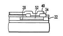
In accordance with the present invention, it may be
desirable to connect the gate po]ysilicon of a desired
device to the source or drain of the same device or that
of another. This can be accomplished during the
deposition and formation of the gate polysilicon. Prior
to the deposition of the gate po]ysilicon 40, a selective
RIE etch ~s carried out to operl a via at a desired
location or locations in iso]ation pad 34, as shown in
Fig. 2, to expose a desired conductor or interconnect 52.
Upon subsequent deposit,i,on and etching of the gate
polysilicon, the gate polysi]i CQn i. S connected to the
conductor or interconnect 52. An additional advantage of
the present invention is that during deposition of the
polysilicon to form the gate polysilicon, any desired
connections between a gate, sollrce, or drain can be made
all in one step, prior to source/drain implants.
In an alternate embodiment of the present invention,
a wafer structure and method of making the same are
substantially similar to t,he preferred embodiment with
the following differences. Prlor to the formation of
isolation pads 22, conductive int,erconnection pads 24 and
interconnection pad caps 2~ are formed on the top surface
of the primary substrate '~ according to the
predetermined int,erco]lnec~,if)rl pa~-terll. This can be
accomplished by the deposit:io~ a blanket layer of
conductive material followed by ~3epo3ition of a blanket
layer of polysilicon and t-hen RT~ etching the pattern of
the conductive interconnect,ion pads 24 and
interconnection pad caps 28 according to the
predetermined interconnection p~ttern. A blanket layer
of isolation material i3 thereaft,er deposited upon the
interconnection pads 24 and the in-terconnection pad caps
28 and subsequently planarized, by any suitable
technique, to form isolation pads 22. (See Fig. l(c))
In yet another alternate embodiment of the present
invention, a wafer strucl,ure ancl method o making the
same are substantially simi]aJ- to the preferred
embodiment with the following differences. Prior to the

FI9-92-041 210S039

formation of iso]atioll pa.ds 22, conductive
interconnection pads 24 are formed on the top surface of
the primary substrate 20 according to the predetermined
interconnection pattern. Thi.s can be accomplished by the
deposition of a blanket layer of conductive material and
then RIE etching the pattern of the conductive
interconnection pads 24 according to the predetermined
interconnection pattern. An isolation material is then
blanket deposited, filling the spaces between conductive
interconnection pads 24 and further covering the top
surfaces of pads 24. The isolation material is
thereafter planarized, for example, by
chemical-mechanical pol.ishing to produce isolation pads
22 and interconnection pad caps 2~. In this embodiment,
the isolation pads 22 and interconnection pad caps 28
comprise the same material and are made at the same time,
thus simplifying the manufactur:e thereof. (See Fig.
(C) )
Referring now to F.ig 3, a top view of a
differential amplifier layou.t with the buried
interconnect structl.lre according to the present invention
is shown. Fig. 4 shows the idelltical layout but with a
conventional l.ocal interconnect plus first metal
interconnect. It can he clearly seen that the
interconnect accordi.ng to the present invention reduces
the layout by approximate].y forty percent (40%) over that
produced by the conventional method. A "semi-global"
wiring pattern for provid~ g pOW~J supply 54 and ground
56 wirings can also be provided according to the
interconnect structure of the present invention. See
Fig. 3.
There is thus provided a planar local interconnect
structure and a method of making the same which are
improvements over conventiona] interconnect structures.
In addition to those advantages already stated, the
planar interconnect structule of the present invention
further simplif.ies the Back End of Line (BEOL)
manufacturing process. ~.s a res~1]t of fabricating the
interconnect structure prior to devi.ce fabrication, no

~ FIg-92-04l 2I O S ~ 39 ~

1 ~
damage occurs to device areas ~nd unwanted conductive
sidewalls are also eliminated.
While the invention has been particularly shown and
described with reference to the preferred embodiment
thereof, it will be unders100d by those skilled in the
art that various changes in form and detail may be made
therein without departin.g from the spirit and scope of
the invention.

Representative Drawing
A single figure which represents the drawing illustrating the invention.
Administrative Status

For a clearer understanding of the status of the application/patent presented on this page, the site Disclaimer , as well as the definitions for Patent , Administrative Status , Maintenance Fee  and Payment History  should be consulted.

Administrative Status

Title Date
Forecasted Issue Date 1996-10-29
(22) Filed 1993-08-27
Examination Requested 1993-08-27
(41) Open to Public Inspection 1994-05-07
(45) Issued 1996-10-29
Deemed Expired 2004-08-27

Abandonment History

There is no abandonment history.

Payment History

Fee Type Anniversary Year Due Date Amount Paid Paid Date
Application Fee $0.00 1993-08-27
Registration of a document - section 124 $0.00 1994-03-04
Maintenance Fee - Application - New Act 2 1995-08-28 $100.00 1995-05-09
Maintenance Fee - Application - New Act 3 1996-08-27 $100.00 1996-06-26
Maintenance Fee - Patent - New Act 4 1997-08-27 $100.00 1997-05-28
Maintenance Fee - Patent - New Act 5 1998-08-27 $150.00 1998-05-14
Maintenance Fee - Patent - New Act 6 1999-08-27 $150.00 1999-05-17
Maintenance Fee - Patent - New Act 7 2000-08-28 $150.00 2000-05-25
Maintenance Fee - Patent - New Act 8 2001-08-27 $150.00 2000-12-15
Maintenance Fee - Patent - New Act 9 2002-08-27 $150.00 2002-06-25
Owners on Record

Note: Records showing the ownership history in alphabetical order.

Current Owners on Record
INTERNATIONAL BUSINESS MACHINES CORPORATION
Past Owners on Record
BUTI, TAQI NASSER
HSU, LOUIS LU-CHEN
JOSHI, RAJIV VASANT
SHEPARD, JOSEPH FRANCIS
Past Owners that do not appear in the "Owners on Record" listing will appear in other documentation within the application.
Documents

To view selected files, please enter reCAPTCHA code :


To view images, click a link in the Document Description column. To download the documents, select one or more checkboxes in the first column and then click the "Download Selected in PDF format (Zip Archive)" or the "Download Selected as Single PDF" button.

List of published and non-published patent-specific documents on the CPD .

If you have any difficulty accessing content, you can call the Client Service Centre at 1-866-997-1936 or send them an e-mail at CIPO Client Service Centre.


Document
Description 
Date
(yyyy-mm-dd) 
Number of pages   Size of Image (KB) 
Representative Drawing 1998-09-15 1 2
Description 1995-06-10 10 538
Cover Page 1995-06-10 1 93
Abstract 1995-06-10 1 80
Claims 1995-06-10 10 488
Drawings 1995-06-10 2 81
Cover Page 1996-10-29 1 18
Abstract 1996-10-29 1 126
Description 1996-10-29 10 520
Claims 1996-10-29 9 763
Drawings 1996-10-29 2 36
Prosecution Correspondence 1996-01-29 2 49
Examiner Requisition 1995-11-21 2 58
Office Letter 1996-03-16 2 45
Office Letter 1996-03-15 1 17
PCT Correspondence 1996-08-16 1 38
Fees 1996-06-26 1 56
Fees 1995-05-09 1 62