Note: Descriptions are shown in the official language in which they were submitted.
WO94/03033 2 1 1 8 9 3 3 PCI/US93/06632
-- 1 --
POWER SUPPLY CIRCUIT
Field of the Invention
This invention relates to power supply
circuits,and particularly, though not exclusively, to
power supply circuits for use in driving gas discharge --
lamp loads.
Background of the Invention
In circuits for driving gas discharge lamp loads,
such as fluorescent lamps, it is known to reduce the
power from which the lamps are driven (so as to
produce dimming of the lamps) by using a resonant
inductor and capacitor in series with the lamps and by
varying the circuit's operating frequency. In such a
known circuit, when the operating frequency of the
circuit is changed, current through the lamps is
reduced and the lamps are correspondingly dimmed.
However, employing variation of the circuit's
operating frequency in order to produce dimming
renders the actual ~ ng level of the circuit
susceptible to changes in the circuit's temperature
which cause the circuit's operating frequency to
change.
Brief Description of the Drawings
FIG. 1 shows a schematic circuit diagram of a
driver circuit for driving three fluorescent lamps;
and
W094/03033 PCT/US93/~32
21189~,3 2 -
FIG. 2 shows a detailed schematic circuit diagram
of a control circuit used in the driver circuit of
FIG. 1.
Description of the Preferred Embodiment
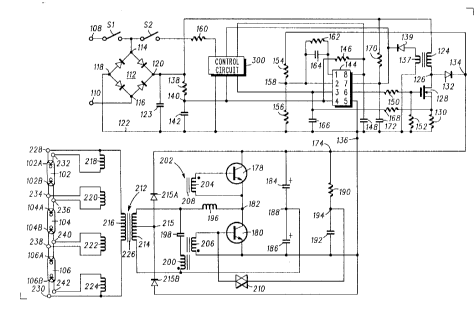
Referring now to FIG. 1, a circuit 100, for
driving three fluorescent lamps 102, 104, 106, has two
input terminals 108, 110 for receiving thereacross an
AC supply voltage of approximately 277V at a frequency
of 60Hz. A full-wave rectifying bridge circuit 112
has two input nodes 114, 116 and has two output nodes
118, 120. The input node 114 is connected to the
input terminal 108 via a conventional two-pole, single
throw "ON-OFF" switch S1 having an element (not shown)
which is mechanically movable between "open" and
"closed" positions. The input node 116 is connected
directly to the input terminal 110. The output node
118 of the bridge 112 is connected to a ground voltage
rail 122. A capacitor 123 (having a value of
approximately 0.18~F) is connected between the output
nodes 118 and 120 of the bridge circuit 112.
A cored inductor 124 (having an inductance of
approximately 4.5mH) has one end connected to the
output node 120 of the bridge 112, and has its other
end connected to a node 126. A field effect
transistor (FET) 128 (of the type BUZ90) has its drain
electrode connected to the node 126. The field effect
transistor (FET) 128 has its source electrode
connected, via a resistor 130 (having a value of
approximately 1.6n), to the ground voltage rail 122.
A diode 132 (of the type MUR160) has its anode
connected to the node 126 and has its cathode
connected to an output node 134. The ground voltage
rail 122 is connected to an output node 136.
W094/03033 2 I 1 8 9 3 3 PCT/US93/ ~ 32
A resistor 138 (having a resistance of
~ approximately 2Mn) is connected between the output
node 120 of the bridge 112 and a node 140. A
capacitor 142 (having a capacitance of approximately
0.0039~F) is connected between the node 140 and the
ground voltage rail 122. A current-mode control
integrated circuit (IC) 144 (of the type AS3845,
available from ASTEC Semiconductor) has its RT/CT
input (pin 4) connected to the node 140. The current
mode control IC 144 has its VREG output (pin 8)
connected, via a resistor 146 ~having a resistance of
approximately loRQ)~ to the node 140 and connected,
via a capacitor 148 (having a capacitance of
approximately 0.22~F) to the ground voltage rail 122.
The current mode control IC 144 has its control signal
output (pin 6) connected, via a resistor 150 (having a
resistance of approximately 20Q), to the gate
electrode of the FET 128. The gate electrode of the
FET 128 is also connected, via a resistor 152 (having
a resistance of approximately 22KQ)~ to the ground
voltage rail 122.
Two resistors 154, 156 (having respective
resistances of approximately 974Kn and 5.36KQ) are
connected in series, via an intermediate node 158,
between the output terminal 134 and the ground voltage
rail 122. The current mode control IC 144 has its VFB
input (pin 2) connected to the node 158. The current
mode control IC 144 has its COMP output (pin 1)
A connected to its VFB input (pin 2) via a parallel-
connected resistor 162 (having a resistance of
approximately 1.5MQ) and capacitor 164 (having a
capacitance of approximately 0.22~F). The current
mode control IC 144 has its current sense input (pin
3) connected to the ground voltage rail 122 via a
- - 21 1 8933
capacitor 166 (having a capacitance of approximately
470pF) and to the source electrode of the FET 128 via
a resistor 168 (having a resistance of approximately
lKQ) .
The current mode control IC 144 has its Vcc input
~pin 7) connected to the bridge rectifier output node
120 via a resistor 170 (having a resistance of
approximately 240~Q) and connected to the ground
voltage rail 122 via a capacitor 172 (having a
capacitance of approximately lOO~F). The current mode
control IC 144 has its GND input (pin 5) connected to
the ground voltage rail 122. A winding 137, wound on
the same core as the inductor 124, has one end
connected to the ground voltage rail 122 and has its
other end connected via a diode 139 to the Vcc input
(pin 7) of the IC 144.
The power supply output terminals 134 and 136 are
connected to input nodes 174 and 176 of a half-bridge
inverter formed by two npn bipolar transistor 178 and
180 (each of the type BUL45). The transistor 178 has
its collector electrode connected to the input node
174, and has its emitter electrode connected to an
output node 182 of the inverter. The transistor 180
has its collector electrode connected to the node 182,
and has its emitter electrode connected to the input
node 176. Two electrolytic capacitors 184 and 186
(each having a value of approximately 47~F) are
connected in series between the inverter input nodes
174 and 176 via an intermediate node 188. For reasons
which will be explained below, a resistor 190 (having
a value of approximately 2.2Mn) and a capacitor 192
(having a value of approximately O.l~F) are connected
in series between the inverter input nodes 174 and 176
via an intermediate node 194.
W094/0~33 PCT/US93/06632
211~33
-- 5 --
The inverter output node 182 is connected to a
series-resonant tank circuit formed by an inductor 196
~having a value of approximately 5.35mH) and a
capacitor 198 (having a value of approximately lOnF).
The inductor 196 and the capacitor 198 are connected
in series, via a primary winding 200 of a base-
coupling transformer 202 which will be described more
fully below, between the inverter output node 182 and
the node 188. The base-coupling transformer 202
includes the primary winding 200 (having approximately
8 turns) and two secondary windings 204 and 206 (each
having approximately 24 turns) wound on the same core
208. The secondary windings 204 and 206 are connected
with opposite polarities between the base and emitter
electrodes of the inverter transistors 178 and 180
respectively. The base electrode of the transistor
180 is connected via a diac 210 ~having a voltage
breakdown of approximately 32V) to the node 194.
An output-coupling transformer 212 has its
primary winding 214 connected in series with the
inductor 196 and in parallel with the capacitor 198
and the primary winding 200 of the base-coupling
transformer 202 to conduct output current from the
tank circuit formed by the series-resonant inductor
196 and capacitor 198. The primary winding 214 of the
transformer 212 is center-tapped at a node 215, which
is coupled to the inverter input nodes 174 and 176 via
diodes 215A and 215B respectively.
The ouL~u~-coupling transformer 212 includes the
primary winding 214 (having approximately 70 turns), a
principal secondary winding 216 (having approximately
210 turns) and four filament-heating secondary
windings 218, 220, 222 and 224 (each having
W094/03033 PCT/US93/06632
2118933
-- 6
approximately 3 turns) wound on the same core 226.
The principal secondary winding 216 is connected
across output terminals 228 and 230, between which the
three fluorescent lamps 102, 104 and 106 are connected
in series. The lamps 102, 104 and 106 each have a
pair of filaments 102A & 102B, 104A & 104B and 106A &
106B respectively located at opposite ends thereof.
The filament-heating secondary winding 218 is
connected across the output terminal 228 and an output
terminal 232, between which the filament 102A of the
lamp 102 is connected. The filament-heating secondary
winding 220 is connected across output terminals 234
and 236, between which both the filament 102B of the
lamp 102 and the filament 104A of the lamp 104 are
connected in parallel. The filament-heating secondary
winding 222 is connected across output terminals 238
and 240, between which both the filament 104B of the
lamp 104 and the filament 106A of the lamp 106 are
connected in parallel. The filament-heating secondary
winding 224 is connected across the output terrl n~ 1
230 and an output term;n~l 242, between which the
filament 106B of the lamp 106 is connected.
A second conventional two-pole, single throw
switch S2, like the switch S1, having an element (not
shown) which is mechanically movable between "open"
and "closed" positions, is connected between the node
114 and a resistor 160 (having a value of
approximately 1 ~ ). As will be explained below, the
switch S2 functions as a "HIGH-LOWn switch.
Referring now also to FIG. 2, the driver circuit
00 also includes a control circuit 300. The control
circuit 300 has a resistive divider formed by a
resistor 302 (having a value of approximately 22Kn)
and a resistor 304 (having a value of approximately
W094/03033 2 1 ~ 8 9 3 3 PCT/US93/06632
47Kn) connected in series between the resistor 160 and
the ground voltage rail 122 (which is connected to pin
5 of the current mode control IC 144) via an
intermediate node 306. A diode 308 has its cathode
electrode connected to the resistor 160 and has its
anode electrode connected to the ground voltage rail
122.
A resistive divider formed by a resistor 310
(having a value of approximately 22RQ) and a resistor
312 (having a value of approximately lOKn) connected
in series between pin 8 of the current mode control IC
144 and the ground voltage rail 122 via an
intermediate node 314. A capacitor 315 (having a
value of approximately 33mF) is connected between pin
8 of the current mode control IC 144 and the cathode
electrode of the diode 308.
An npn bipolar transistor 316 (of the type 2N3904) has
its base electrode connected to the node 306, has its
collector electrode connected to the node 314, and has
its emitter electrode connected to the ground voltage
rail 122.
A further npn bipolar transistor 318 (of the type
2N3904) has its base electrode connected to the node
314, and has its emitter electrode connected to the
ground voltage rail 122. A resistive divider formed
by a resistor 320 (having a value of approximately
4.7 ~ ) and a resistor 322 (having a value of
approximately 22Kn) connected in series between pin 7
of the current mode control IC 144 and the collector
electrode of the transistor 316 via an intermediate
node 324. A pnp bipolar transistor 326 (of the type
2N3906) has its base electrode connected to the node
324, and has its emitter electrode connected to pin 7
21 18933
of the current mode control IC 144. A tapped,
variable resistor 328 (having a nominal value of 20KQ)
is connected between the collector electrode of the
transistor 326 and the ground voltage rail 122.
The tapped terminal of variable resistor 328 is
connected to pin 3 of the current mode control IC 144
via a resistor 330 ~having a value of approximately
5~llKQ)~ a diode 332 (of the type lN4148) and a
resistor 334 (having a value of approximately 11.3K
connected in series. A resistor 336 (having a value
of approximately 14.3KQ)~ a diode 338 (of the type
lN4148) and a capacitor (having a value of
approximately l~F) are connected in series between pin
4 of the current mode control IC 144 and the ground
voltage rail 122. The anode electrodes of the diodes
332 and 338 are connected together.
The integrated circuit 144 and its associated
components form a voltage-boost circuit which operates
a. a frequency of nominally 23KHz and produces, when
activated, a boosted output voltage between the output
terminals 134 and 136.
The transistors 178 and 180, the inductor 196,
the capacitor 198 and their associated components form
a self-oscillating inverter circuit which produces,
when activated, a high-frequency (e.g. 40KHz) AC
voltage across the primary winding 214 of the output-
coupling transformer 212. The voltages induced in the
secondary windings 218, 220, 222 and 224 216 of the
A~. ''~ '
21 18933
output-coupllng transformer serve to heat the lamp
filaments 102A & 102B, 104A & 104B and 106A & 106B and
the voltage lnduced in the secondary winding 216 of
the output-coupling transformer serves to drlve
current through the lamps 102, 104 and 106.
. .
In operation of the circuit of FIG. 1, with the
switches S1 and S2 closed and with a voltage of 277V,
60Hz applied across the input terminals 108 and 110,
the bridge 112 produces between the node 120 and the
ground voltage rail 122 a unipolar, full-wave
rectified, DC voltage having a frequency of 120Hz.
When the circuit is first powered-up, the
activation of the voltage-boost IC 144 is controlled,
for reasons which will be explained below, by the
resistive-capacitive divider 170, 172 connected
between the output nodes 118 and 120 of the bridge
circuit 112. The component values in the preferred
embodiment of the circuit of FIG. 1 are chosen to
produce a delay of approximately 0.7 seconds between
initial power-up of the circuit and activation of the
voltage-boost IC 144. Similarly, when the circuit is
first powered-up, the activation of the self-
oscillating inverter is controlled by the resistive-
capacitive divider 190, 192 connected between the
output terminals 134 and 136 of the voltage-boost
circuit formed by the IC 144 and its associated
components. The component values in the preferred
embodiment of the circuit of FIG. 1 are chosen to
~ ~ .
W094/03033 PCT/US93/ ~ 32
2118933
-- 10 --
produce a delay of approximately 40 milliseconds
between initial power-up of the circuit and activation
of the self-oscillating inverter.
The circuit of FIG. 1 is so arranged that, with
the self-oscillating inverter activated but before
activation of the voltage-boost IC 144, an unboosted
voltage of approximately 390V appears across the
output terminals 134 and 136, and the voltage induced
in the secondary windings 118, 120, 122 and 124 iS
sufficient to produce significant heating of the
filaments 102A & 102B, 104A & 104B and 106A & 106B,
but the voltage induced in the secondary winding 216
is insufficient to cause the lamps to strike.
15 However, after activation of the voltage-boost IC 144,
a boosted voltage of approximately 458V appears across
the output terminals 134 and 136 and the voltage
induced in the secondary windings 118, 120, 122 and
124 continues to heat the filaments and the voltage
20 induced in the secondary winding 216 is sufficient to
cause the lamps to strike.
Thus, by arranging that ~i) the unboosted voltage
across the output ter~; nA 1 s 134 and 136 causes heating
of the filaments 102A & 102B, 104A & 104B and 106A &
106B but no striking of the lamps 102, 104 and 106,
(ii) there is a delay of approximately 2/3 seconds
(0.66 = 0.7 - 0.04) seconds between activation of the
self-oscillating inverter and activation of the
30 voltage-boost circuit; and (iii) the boosted voltage
across the output terminals 134 and 136 causes
striking of the lamps 102, 104 and 106 as well as
continued heating of the filaments 102A & 102B, 104A &
104B and 106A & 106B, the circuit of FIG. 1 simply and
35 effectively produces pre-heating of the lamp filaments
before the lamps are caused to strike.
~ I 1 8933
The control circuit 300 controls ~imming
operation of the drive circuit 100 in dependence on
the operation of the "HIGH-LOW" switch S2 as follows.
With the switch S2 in its CLOSED or HIGH position,
when the circuit is powered up by closing the switch
S1 pulsating D.C. voltage from the node 114 appears at
the cathode electrode of the diode 308. This
pulsating voltage is filtered by the capacitor 315 and
causes the diode 308 to be reverse biased and results
in the production of a steady voltage of approximately
5V across the resistors 302 and 304. In this
condition, the transistor 316 will be turned ON,
pulling low the node 314 and causing the transistor
318 to be turned OFF. With the transistor 318 turned
OFF, the transistor 326 is prevented from turning ON.
Thus, in this condition with the transistor 318 turned
OFF, no bias is applied through the tap terminal of
the variable resistor 328 to pins 3 or 4 of the
voltage boost IC 144. The lack of D.C. bias at pins 3
and 4 of the boost IC 144 allows the voltage boost IC
to operate in its normal manner at full power.
I~ the "HIGH-LOW" switch S2 is placed in its OPEN
or LOW position while the circuit is operating, the
voltage at the cathode electrode of the diode 308
falls from its value of approximately 5V as the
capacitor 315 discharges through the resistor 302.
When the voltage across the resistor 304 falls below
W094/03033 PCT/US93/ ~ 32
2118933
- 12 -
approximately 0.6V, the transistor 316 is turned OFF,
allowing the node 314 to rise high and causing the
transistor 318 to be turned ON. With the transistor
318 turned ON, the node 324 is pulled low and the
transistor 326 is turned ON. Thus, in this condition
with the transistor 318 turned ON, D.C. bias is
applied through the tap terminal of the variable
resistor 328 to pins 3 and 4 of the voltage boost IC
144. The D.C. bias at pin 3 (the "CURRENT SENSE"
input) of the boost IC 144 causes a reduction in the
power that the voltage boost IC produces, causing the
lamps 102, 104, 106 to dim to a predetermined LOW
light level. As will be explained in greater detail
below, at the same time, the D.C. bias at pin 4 (the
"FREQUENCY CONTROL" input) of the boost IC 144 causes
an increase in the frequency at which the voltage
boost IC operates.
When the D.C. bias is applied to pin 3 of the
voltage boost IC 144 to limit its power output and so
produce ~;~ming of the lamps 102, 104, 106, the power
factor of the circuit will otherwise be reduced from
its optimum value since the voltage boost IC 144 is
being forced to operate at less than its full power
level for which its design was optimized. In order to
correct for this fall in power factor, the D.C. bias
is applied to pin 4 of the voltage boost IC so as to
increase the voltage boost IC's frequency of operation
commensurate with the reduced power. The effect of
increasing the voltage boost IC's frequency of
operation commensurate with its reduced power output
is to compensate for the associated fall in power
factor, thereby retain retaining a substantially
constant, optimum power factor for the circuit in both
the HIGH power (or full light) and LOW power (or
dimmed light) states.
WOg4/03033 2 1 1 8 9 3 3 PCT/US93/~32
It will be appreciated that the circuit described
provides dimming of the lamps without varying the
frequency at which the lamps are driven, this
S frequency remaining substantially constant at
approximately 40KHz as described above. Thus, the
circuit provides dimming which is not susceptible to
variation of the circuit's operating temperature.
It will also be appreciated that the above
circuit allows dimming to be performed efficiently and
simply, the control circuit 300 requiring components
which are simple and few in number. It will also be
appreciated that in the above circuit, dimming can be
simply and effectively provided as an add-on or retro-
fit feature by adding the additional switch "HIGH-LOW"
switch S2 and the control circuit 300: without these
additional components the circuit operates as a
conventional fixed-light-level ballast circuit.
It will also be understood that although the
above circuit has been described as operating in only
a HIGH power (or full light) mode and a predetermined
LOW power ~or dimmed light), the power or light level
of the LOW power mode can be varied, e.g., by
adjusting the variable resistor 328, to produce any of
a desired range of dimmed lighting levels. It will be
understood that the power factor of the circuit
remains substantially constant throughout variation
of the LOW power level in this way, since the D.C.
bias applied at pin 4 of the voltage boost IC 144 to
increase its frequency of operation is commensurate
with the D.C. bias applied at pin 3 to reduce the IC's
power output.
W094/03033 PCT/US93/06632
2118933
- 14 -
It will be appreciated that the component values
used in the above described circuit, and the
particular voltage levels may be varied as desired to
suit different types of fluorescent or other gas
discharge lamps as desired.
It will also be appreciated that although the
invention has been described above in relation to a
power supply for a circuit used to drive lighting
units, the invention is not limited to use in
connection with lighting units and may be used equally
well as a power supply in other applications.
It will be appreciated that various other
modifications or alternatives to the above described
embodiment will be apparent to a person skilled in the
art without departing from the inventive concept.