Note: Descriptions are shown in the official language in which they were submitted.
CA 02151291 2004-06-21
LIQUID CRYSTAL DISPLAY HAVING
HIGH CONTRAST VIEWING ZONE
CENTERED IN POSITIVE OR NEGATIVE VERTICAL REGION
This invention relates to a liquid crystal display
having at least one retardation film. More particularly,
this invention relates to a normally white liquid crystal
display including a retardation film disposed on one side
of the liquid crystal layer, the optical axis of the
retardation film being oriented according to the
manufacturer's desired specification.
RELATED APPLICATIONS
This is a continuation-in-part of U.S. Serial No.
08/167,652 filed December 15, 1993, now issued as U.S.
Pat. No. 5,570,214, and U.S. Serial No. 08/235,691 filed
April 29, 1994, now issued as U.S. Pat. No. 5,594,568.
BACKGROUND OF THE INVENTION
Liquid crystal materials are useful for electronic
displays because light traveling through a layer of
liquid crystal (LC) material is affected by the
anisotropic or birefringent value (A n) of the LC material
which in turn can be controlled by the application of a
voltage across the LC. Liquid crystal displays (LCDs)
are commonly used in applications such as avionic cockpit
displays, portable computers, calculators, etc.
~~~1~~1
Informational data in typical liquid crystal
displays is presented in the form of a matrix array of
rows and columns of numerals or characters which are
generated by a number of segmented electrodes arranged in
a matrix pattern. The segments are connected by
individual leads to driving electronics which apply a
voltage to the appropriate combination of segments and
adjacent LC material in order to display the desired data
and/or information by controlling the light transmitted
through the liquid crystal material.
Contrast ratio is one of the most important
attributes considered in determining the quality of both
normally white (NW) and normally (NB) liquid crystal
displays. The contrast ratio in a normally white display
is determined in low ambient conditions by dividing the
"off-state" light transmission (high intensity white
light) by the "on-state" or darkened transmitted
intensity. For example, if the "off-state" transmission
is 200 fL at a particular viewing angle and the "on-
state" transmission is 5 fL at the same viewing angle,
then the display's contrast ratio at that particular
viewing angle is 40 or 40:1 for the particular "on-state"
driving voltage utilized.
Accordingly, in normally white LCDs the primary
factor adversely limiting the contrast ratio is the
amount of light which leaks through the display in the
darkened or "on-state". In a similar manner, in normally
2
~1~~29I
black displays, the primary factor limiting the contrast
ratio achievable is the amount of light which leaks
through the display in the darkened or "off-state". The
higher and more uniform the contrast ratio of a
particular display over a wide range of viewing angles,
the better the LCD.
Normally black (NB) twisted nematic displays
typically have better contrast ratio contour curves or
characteristics then do their counterpart NW displays in
that the NB image can be seen better at large viewing
angles. However, NB displays are much harder to
manufacture than NW displays due to their high dependence
on the cell gap or thickness "d" of the liquid crystal
layer as well as on the temperature of the liquid crystal
material itself. Accordingly, a long-felt need in the
art has been the ability to construct a normally white
display with high contrast ratios over a large range of
viewing angles, rather than having to resort to the more
difficult to manufacture NB display to achieve these
characteristics.
What is generally needed in NW displays is an
optical compensating or retarding element(s), i.e.
retardation film, which introduces a phase delay that
restores the original polarization state of the light,
thus allowing the light to be substantially blocked by
the output polarizes in the "on-state". Optical
compensating elements or retarders are known in the art
3
CA 02151291 2005-05-25
and are disclosed, for example, in U.S. Pat:. Nos.
5,184,236, 5,196,953, 5,138,474, and 5,071,997.
Figure 1 is a contrast ratio curve graph for a prior
art normally white twisted nematic light valve'including a
rear linear polarizer having a transmission axis oriented
in a first direction, a front or light exit. linear
polarizer having a transmission axis defining a second
direction wherein the first and second directions are
substantially perpendicular to one another, a liquid
crystal material having a cell gap "d" of about 5.86 um and
a birefringence (fin) of about 0.084 at room temperature, a
rear buffing or orientation film buffed in the second
direction, and a front orientation film buf=fed'-in the first
direction. The temperature at which Figure 1 was developed
was about 34.4°C. This light valve did not. include a
retarder.
The contrast ratio curves of Figure 1 were plotted
utilizing a 6.8 volt "on-state" driving vo7_tage, a 0.2 volt
'°off-state" or VoFF voltage, and by convent~_onally
backlighting the display with white light. As can be seen
in Figure 1, the viewing zone or envelope of the light
valve while being fairly broad horizontall~r in the lower
vertical region becomes narrowed or constructed in the
positive vertical viewing region. For example, at positive
20° vertical, the 10:1 and greater contrast.
4
ratio region extends horizontally over only a total of
about 70° while at -20° vertical, this same 10:1 contrast
ratio zone extends over a horizontal total of about 100°.
Therefore, because of the non-uniform or skewed shape of
the viewing zone or envelope shown in Figure 1, it is
evident that viewers in the positive vertical viewing
region will have difficulty viewing displayed images at
medium and large horizontal viewing angles such as about
t40°. This graph is illustrative of the common problems
associated with typical normally white liquid crystal
displays in that their contrast ratios are limited at
increased horizontal and vertical viewing angles.
Figure 2 is a driving voltage versus intensity (fL)
plot of the prior art light valve described above with
respect to Figure 1, this plot illustrating the gray
level behavior of this light valve. The various curves
represent horizontal viewing angles from about -60° to
+60° along the 0° vertical viewing axis.
Gray level performance and the corresponding amount
of inversion are important in determining the quality of
an LCD. Conventional liquid crystal displays typically
utilize anywhere from about 8 to 64 different driving
voltages. These different driving voltages are generally
referred to as "gray level" voltages. The intensity of
light transmitted through the pixels) or display depends
upon the driving voltage utilized. Accordingly,
conventional gray level voltages are used to generate
5
2~ ~~ ~JI
dissimilar shades of color so as to create different
colors when, for example, the shades are mixed with one
another. -
Preferably, the higher the driving voltage in a
normally white display, the lower the intensity (fL) of
light transmitted therethrough. Likewise then, the lower
the driving voltage, the higher the intensity of light
reaching the viewer. The opposite is true in normally
black displays. Thus, by utilizing multiple gray level
driving voltages, one can manipulate either a NW or NB
liquid crystal display to emit desired intensities and
shades of light/color. A gray level VoN is generally
known as any driving voltage greater than Vth (threshold
voltage) up to about 5 - 6.5 volts.
Gray level intensity in LCDs is dependent upon the
display's driving voltage. It is desireable in NW
displays to have an intensity versus driving voltage
curve wherein the intensity of light emitted from the
display or pixel continually and monotonically decreases
as the driving voltage increases. In other words, it is
desireable to have gray level performance in an NW pixel
such that the intensity (fL) at 6.0 volts is less than
that at 5.0 volts, which is in turn less than that at 4.0
volts, which is less than that at 3.0 volts, which is in
turn less than that at 2.0 volts, etc. Such desired gray
level curves across wide ranges of view allow the
intensity of light reaching viewers at different viewing
6
~~~j2~I
angles via the pixels) or display to be easily and
consistently controlled.
Turning again to Figure 2, the intensity versus
driving voltage curves illustrated therein of the Figure
1 light valve having no retardation film are undesireable
because of the inversion humps present in the areas of
the curves having driving voltages greater than about 3
or 3.2 volts. The intensity aspect of the curves
monotonically decreases as the driving voltage increases
in the range of from about 1.6 - 3.0 volts, but at a
driving voltage of about 3.2 volts, the intensities at a
plurality of viewing angles begin to rise as the voltage
increases from about 3.2 volts up to about 6.8 volts.
Such rises in intensity as the driving voltage increases
are known as "inversion humps". Inversion humps lead to
the display or light valve emitting different colors via
the same pixel at different viewing angles for the same
driving voltage. Clearly, this is undesirable. Whilte
the inversion humps of Figure 2 include only rise
portions, inversion humps often include both rise and
fall portions as will be appreciated by those of ordinary
skill in the art, thus enabling the "inversion humps" to
actually look like humps.
A theoretically perfect driving voltage versus
intensity (fL) curve for an NW display would have a
decreased intensity (fL) for each increase in gray level
driving voltage at all viewing angles. In contrast to
7
CA 02151291 2005-05-25
this, the inversion humps of Figure 2 represent large
increases in intensity of radiation emitted from the light
valve for each corresponding increase in gx-ay level driving
voltage above about 3.2 volts. Accordingly, it would
satisfy a long-felt need in the art if a normally white
liquid crystal display could be provided with no or little
inversion.
U.S. Pat. No. 5,184,236 discloses an r~nT display
including a pair of retardation films provided on one side
of the LC layer, these retardation films having retardation
values of about 300 nm or greater. The viewing
characteristics of the LCDs of this patent could be
improved upon with respect to contrast ratio, inversion,
and uniformity as well as the position of the viewing zone
by utilizing retarders of different values and
orientations. Furthermore, it is felt that such
improvements may be achieved with a reduced number of
retardation films thus reducing the cost and complexity of
the display.
The parents of this application, now issued as U.S.
Pat. Nos. 5,570,214 and 5,594,568 provide f_or NW displays
with a pair of retardation films having retardation values
of about 80-200 nm. t~h.ile the different embodiments of
U.S. Pat. Nos. 5,570,214 and 5,594,568 provide excellent
results with respect to viewing characteri:~tics, the
disclosure of this application allows improved viewing
characteristics in
8
2~~~29I
the vertical viewing regions while sacrificing certain
viewing characteristics at other viewing angles.
Figure 3 illustrates the angular relationships
between the horizontal and vertical viewing axes and
angles described herein relative to a liquid crystal
display and conventional LCD angles ~ and e. The +X, +Y,
and +Z axes shown in Figure 3 are also defined in other
figures herein. Furthermore, the "horizontal viewing
angles" (or XANG) and "vertical viewing angles" (or YpN~)
illustrated and described herein may be transformed to
conventional LCD angles: azimuthal angle ~: and polar
angle e, by the following equations:
Tan (xqNG) - Cosine (cp) ~ Tan (e)
sine (YANG) - sine (e) ~ sine (cp)
or
Cosine (6) - Cosine (YANG) ' Cosine (RANG)
Tan (~) - Tan (YANG) . Sine (XANC)
The term "rear" when used herein but only as it is
used to describe substrates, polarizers, electrodes,
buffing zones, and orientation films means that the
described element is on the backlight side of the liquid
crystal material, or in other words, on the side of the
LC material opposite the viewer.
The term "front" when used herein but only as it is
used to describe substrates, polarizers, electrodes,
buffing zones and orientation films means that the
9
2~~j2~I
described element is located on the viewer side of the
liquid crystal material.
The LCDs and light valves herein include a liquid
crystal material with a birefringence (ttn) of 0.084 at
room temperature, Model No. ZLI-4718 obtained from Merck.
The term "retardation value" as used herein means
"d - o n" of the retardation film or plate, wherein "d" is
the film thickness and "en" is the film birefringence.
The term "interior" when used herein to describe a
surface or side of elements (or an element itself), means
the side or surface closest to the liquid crystal
material.
The term "light valve" as used herein means a liquid
crystal display including a rear linear polarizer, a rear
transparent substrate, a rear continuous pixel electrode,
a rear orientation film, an LC layer, a front orientation
film, a front continuous pixel electrode, a front
substrate, and a front polarizer (without the presence of
color filters and driving active matrix circuitry such as
TFTs). Such a light valve may also include a retardation
films) disposed on either side of the LC layer as
described with respect to each example and embodiment
herein. In other words, a "light valve" may be referred
to as one giant pixel without segmented electrodes.
It is apparent from the above that there exists a
need in the art for a normally white liquid crystal
display wherein the viewing zone of the display has both
~~ ~~ 2~~
high contrast ratios and little or no inversion over a
wide range of viewing angles, the viewing zones position
being shiftable to different vertical regions so as to
allow viewers at such predetermined viewing angles (e. g.
positive vertical viewing angles) to be able to
satisfactorily view the displayed image.
This invention will now be described with respect to
certain embodiments thereof, accompanied by certain
illustrations wherein:
SUMMARY OF THE INVENTION
Generally speaking this invention fulfills the
above-described needs in the art by providing a method of
shifting the high contrast ratio viewing zone of a
twisted nematic normally white liquid crystal display
upward into the positive or upward vertical viewing zone,
the method comprising the steps of:
a) sandwiching a twisted nematic liquid crystal
layer between a pair of electrodes, the liquid crystal
layer having a thickness of from about 4.5 - 6.5 ~.m;
b) orienting the liquid crystal molecules on a
first side of the liquid crystal layer in a first
direction;
c) orienting the liquid crystal molecules on a
second side of the liquid crystal layer in a second
direction, the first and second directions being
different from one another in a manner such that the
11
CA 02151291 2004-06-21
liquid crystal layer when in the off-state twists at
least one visible wavelength of light less than about
100°;
d) providing a retardation film having a
retardation value "d ~ D n" in the range of about 100-250
nm on the first side of the liquid crystal layer, wherein
"d" is the thickness of the retardation film and " ~ n" is
its birefringence;
e) rotating the optical axis of the retardation
film from about 2° - 20° relative to the second
direction, the rotating of the optical axis shifting the
high contrast viewing zone vertically so that viewers at
such viewing angles may see a high contrast image with
reduced inversion.
This invention further fulfills the above-described
needs in the art by providing a twisted nematic liquid
crystal display capable of displaying an image to a
viewer, the display comprising:
a pair of electrodes sandwiching a twisted nematic
liquid crystal layer therebetween, the pair of electrodes
for applying a voltage across the liquid crystal layer;
first and second orientation means disposed adjacent
the liquid crystal layer on opposite sides thereof, the
first orientation means defining a first orientation or
buffing direction and the second orientation means
defining a second orientation or buffing direction, the
first and second orientation directions for aligning the
12
~~ ~~ 29I
liquid crystal molecules of the liquid crystal layer in a
predetermined manner:
a positively birefringent unaxial retardation film
having a retardation value "d ~ an" in the range of about
100 - 200 nm, where "d" is the thickness of the
retardation film and "an" is its birefringent value,
wherein the retardation film is disposed on the same side
of the liquid crystal layer as the first orientation
means, the retardation film being oriented such that its
optical axis is substantially parallel ~ about 20° to the
second orientation or buffing direction of the second
orientation means thereby enabling the liquid crystal
display to display to the viewer an image with improved
contrast ratios and reduced inversion.
This invention further fulfills the above-described
needs in the art by providing a method of making a
normally white twisted nematic liquid crystal display, a
method comprising the steps of:
a) sandwiching a liquid crystal layer between
first and second electrodes, the liquid crystal layer
having a thickness "d" of from about 4.5 to 6.5 wm:
b) providing a first orientation means between the
first electrode and the liquid crystal layer, the first
orientation means for orienting LC molecules of the LC
layer in a first direction adjacent the first orientation
means:
13
c) providing a second orientation means between
the LC layer and the second electrode, the second
oriEntation means for orienting LC molecules in a second
direction adjacent the second orientation means;
d) disposing a positively birefringent uniaxial
retardation film on the same side of the LC layer as the
first electrode and first orientation means, the
retardation film having a retardation value of from about
100 - 200 nm; and
e) orientating the optical axis of the uniaxial
retardation film substantially parallel ~ about 20° to
the second direction defined by the second orientation
means whereby the normally white display exhibits
improved contrast ratios and reduced inversion.
This invention will now be described with respect to
certain embodiments thereof, wherein:
IN THE DRAWINGS
Figure 1 is a contrast ratio plot of a prior art
light valve which utilized white light and an "on-state"
driving voltage of about 6.8 volts.
Figure 2 is an intensity versus driving voltage plot
of the prior art light valve of Figure 1, this plot
illustrating a fairly large amount of undesireable
inversion over a wide range of horizontal viewing angles
at driving voltages greater than about 3 volts.
14
Figure 3 is a graph illustrating the angular
relationship between the horizontal and vertical viewing
angles discussed herein, and their relationship with
conventional liquid crystal display viewing angles:
azimuthal angle ~; and polar angle e.
Figure 4 is an exploded perspective schematical
diagram of the optical components and their respective
orientations of an LCD according to a first embodiment of
this invention.
l0 Figure 5 is a top view illustrating the optical
component angular relationships of the liquid crystal
display of Figure 4.
Figure 6 is a side elevational cross-sectional view
of the LCD of the first or Figures 4 - 5 embodiment of
this invention.
Figure 7 is an exploded perspective schematical
diagram of the optical components and their respective
orientations of an LCD according to a second embodiment
of this invention, this embodiment being "P-buffed" as
opposed to the "X-buffed" first embodiment.
Figure 8 is an exploded perspective schematical
diagram of the optical components and their respective
orientations of an LCD according to a third embodiment of
this invention wherein the retardation film is disposed
on the rear or backlight side of the liquid crystal
layer.
2~~~2~I
Figure 9 is a white light contrast ratio contour
plot of the normally white Display "A" of Example 1 when
a driving voltage of about 6.8 volts was applied.
Figure 10 is a white light contrast ratio contour
plot of the normally white Display "A" of Example 1 when
utilizing a driving voltage of about 6.0 volts was
applied.
Figure 11 is a white light transmission (fL) versus
driving voltage plot of the normally white Display "A" of
Example 1, this plot illustrating the viewing
characteristics at a plurality of horizontal viewing
angles disposed along the 0° vertical viewing axis.
Figure 12(a) is a white light contrast ratio contour
plot of the comparative normally white Display "B" of
Example 1 when a driving voltage of about 6.8 volts was
applied.
Figure 12(b) is a white light contrast ratio contour
plot of the comparative NW Display "C" of Example 1 when
a driving voltage of about 6 volts was applied.
Figure 13 is a white light contrast ratio contour
plot of the NW light valve of Example 2 when a driving
voltage of about 5.0 volts was applied.
Figure 14 is a white light contrast ratio contour
plot of the NW light valve of Example 2 when a driving
voltage of about 4.0 volts was applied.
16
CA 02151291 2004-06-21
Figure 15 is a white light contrast ratio contour
plot of the normally white AMLCD of Example 3 when a
driving voltage of about 6.0 volts was applied.
DETAILED DESCRIPTION OF
CERTAIN EMBODIMENTS OF THIS INVENTION
Referring now more particularly to the accompanying
drawings in which like reference numerals indicate like
parts.
Figure 4 is an exploded schematic view of the
optical components and their respective orientations of
an LCD according to a first embodiment of this invention,
the LCD being an AMLCD having a matrix array of pixels
and colored subpixels in certain embodiments. As shown,
this display (or display assembly) includes from the rear
forward toward viewer 1, conventional backlight 3, rear
or light-entrance linear polarizer 5, rear buffing or
orientation film 7, liquid crystal layer 9, front buffing
or orientation film 11, retardation film 13, and finally
front or light-exit linear polarizer 15.
Backlight 3 is conventional in nature and emits
substantially collimated light toward the display panel
including rear polarizer 5 in certain embodiments of this
invention. Backlight 3 may be, for example, the
backlighting assembly disclosed in commonly owned U.S.
Pat. No. 5,161,041. Other conventional
17
2j~~2~I
high intensity substantially collimated backlight
assemblies may also be used.
Rear and front polarizers 5 and 15 are linear in
nature in certain embodiments of this invention and their
respective linear transmission axes PR and PF are
orientated such that the displays of the different
embodiments are of the normally white (NW) type.
Therefore, when a driving voltage below the threshold
voltage Vth is applied across liquid crystal layer 9,
transmission axes PR and PF of polarizers 5 and 15
respectively are orientated such that the light emitted
from backlight 3 proceeds through and is linearly
polarized in direction PR by polarizes 5, is then twisted
(e. g. about 80° - 100°) by LC material 9, and finally
exits polarizes 15 via transmission axis PF thus reaching
viewer 1. The light reaches viewer 1 because its
polarization directon upon reaching front polarizes 15 is
similar to that of axis PF. Thus, a NW display or pixel
to which a voltage less than Vth is applied is said to be
in the "off-state" and appears white (or colored if
colored filters are present) to the viewer.
However, when a substantial driving voltage (e. g.
about 6 volts) is applied across selected NW pixels of
the matrix array including liquid crystal layer 9, the
light transmitted through rear polarizes 5 is not
significantly twisted by LC layer 9 and thus is
substantially blocked by front polarizes 15 due to the
18
fact that the polarization direction of light reaching
the interior surface of front polarizes 15 is
substantially perpendicular to transmission axis PF
thereby resulting in substantially no light reaching
viewer 1 by way of the selected pixels to which the
substantial driving voltage is applied. Thus, the
selected pixels driven in the matrix array appear
darkened to viewer 1, these pixels said to be in the "on-
state". As will be appreciated by those of skill in the
art, the amount of light reaching viewer 1 is dictated by
the voltage applied to LC layer 9 - the higher the
driving voltage, the darker the selected driven pixels)
appear.
In certain embodiments of this invention,
transmission axis PR of rear polarizes 5 and transmission
axis PF of front polarizes 15 are oriented in a manner
substantially perpendicular to one another so as to
define a normally white twisted nematic cell. However,
polarizers 5 and 15 may be oriented in other conventional
manners which also allow the cell or display to be of the
normally white type.
Rear and front orientation or buffing films 7 and
11, respectively, are conventional and made of a
substantially transparent polyimide in certain
embodiments of this invention. Rear orientation film 7
is conventionally buffed or oriented in direction BR as
shown in Figure 4. Likewise, front film 11 is
19
2~~I2~1
conventionally buffed in direction BF. Buffing directions
BR and BF are oriented substantially perpendicular to one
another in certain embodiments of this invention so as to
allow the molecules of liquid crystal layer 9 when in the
off or non-driven state to be twisted from about 80° -
100°, most preferably about 90°. The term "off-state"
means that a voltage below the threshold voltage (Vth) is
applied across LC layer 9.
Due to the orientation of buffing directions BR and
BF of orientation films 7 and 11 respectively, the
polarization direction of normally incident light emitted
from backlight 3 reaching liquid crystal material 9 is
twisted in a conventional manner by the liquid crystal
molecules as it passes through layer 9, when, of course,
the display (or selected pixels thereof) is in the off-
state.
However, when a substantially full driving voltage,
e.g. about 6 volts or above, is applied to liquid crystal
layer 9 (or selected pixels thereof to form the intended
image), the normally incident light from backlight 3
reaching layer 9 is permitted to pass therethrough while
substantially maintaining its initial direction of
polarization. This is.due to the fact that when a
voltage is applied across LC material 9, the LC molecules
are caused to become substantially aligned with one
another in the vertical direction as shown in Figure 4.
Therefore, little or substantially no twisting occurs
2~~Z~~~
when such a driving voltage (e.g. about 6 volts) is
applied and thus the direction of polarization of light
passing through layer 9 is substantially maintained.
The voltage amount applied across LC layer 9
determines the degree of twisting of the liquid crystal
molecules and thus dictates the polarization direction of
light emitted from the front or viewer side of layer 9.
In turn, the polarization direction of light reaching
polarizer 15 dictates the amount of light permitted to
pass therethrough via axis PF and reach viewer 1 in that
the closer aligned transmission axis PF and the
polarization direction of light reaching polarizer 15,
the more light which is allowed to pass and reach viewer
1.
While the application of voltage > Vth to layer 9
causes the LC molecule to substantially align vertically,
the LC molecules never completely stand on end or become
perfectly aligned in the vertical direction as is known
in the art. This gives rise to the need for retardation
films) .
Retardation film 13 in this first embodiment is
disposed on the viewer side of liquid crystal layer 9
thereby being sandwiched between front polarizer 15 and
front orientation film 11. Surprisingly, it has been
found that the provision of retardation film 13 on a
single side of twisted nematic LC layer 9 reduces
inversion and improves viewing zone contrast ratios at
21
CA 02151291 2004-06-21
large viewing angles when the retardation value of the
film is reduced relative to the prior art to retardation
values of from about 100-200 nm.
Retardation film 13 in certain embodiments of this
invention is positively birefringent and uniaxial in
nature, this film being obtained from, for example, Nitto
Corporation, Japan, or Nitto Denko America, Incorporated,
New Brunswick, N.J. as Model No. NRF-140 (140 nm
retarder).
Alternatively, it is believed that biaxial
retardation films having similar retardation values may
also provide excellent results, such biaxial retardation
films and values being disclosed in aforementioned U.S.
Pat. No. 5,594,568.
With reference to FIGS. 4-5, axis PR and direction
BF are substantially parallel to one another in
certain embodiments of this invention while direction BR,
axis PF, and direction R (or Ro) are also substantially
parallel ~ about 5° to one another. Accordingly, in such
embodiments, axis PR and direction BR are substantially
perpendicular to one another as are axis PF and direction
BF. A display having such an optical arrangement is said
to be "X-buffed". The term "X-buffed" means that rear
polarizer axis PA is substantially perpendicular to rear
buffing direction BR while front polarizer axis PF is
substantially perpendicular to front buffing direction
BF. Thus, the first embodiment of this invention
22
~~ ~Z 2JI
illustrated in Figures 4 - 6 is an LCD of the "X-buffed"
type.
Alternatively, an LCD may be "P-buffed" instead of
"X-buffed" in certain embodiments, "P-buffed" meaning
that rear polarizer axis PR is substantially parallel to
rear buffing direction BR and front polarizer axis PF is
substantially parallel to front buffing direction BF.
Optical axis R of retardation film 13 in the first
embodiment of this invention (see Figures 4 - 6) may be
aligned in direction Ro so as to be substantially parallel
to axis PF and buffing direction BR. Alternatively,
optical axis R of retardation film 13 may be rotated.
either clockwise or counterclockwise relative to
directions Ro and BR.
The effect of rotating optical axis R of film 13
relative to direction Ro is to shift the viewing zone or
envelope of the display vertically into either the upper
or lower vertical region as will be further discussed in
the examples below. When film 13 is disposed forward of
LC layer 9 and optical axis R of retardation film 13 is
rotated clockwise relative to direction Ro (as shown in
Figures 4 - 5) so as to define angle ~ therebetween, the
high contrast viewing envelope of the display is shifted
into the upper or positive vertical region so as to
provide viewer 1 with a high contrast ratio image at
increased positive vertical viewing angles. To achieve
such a high quality shifted image in the positive
23
vertical region, optical axis R of retardation film 13 is
rotated clockwise (to define e) from about 2° - 20°
relative to Ro, more preferably about 4° - 15°, and most
preferably from about 6° -10° in certain embodiments of
this invention. The term "clockwise" is defined as being
viewed from the position of viewer 1 in Figure 4 (or as
shown in Figures 4 - 5).
Alternatively, optical axis R of film 13 may be
rotated counterclockwise relative to direction Ro so as to
shift the high contrast viewing envelope of the display
into the negative vertical viewing region when film 13 is
positioned forward of LC layer 9. The same degrees of
rotation discussed above relative to clockwise rotation
of axis R also apply to this alternative counterclockwise
rotation of optical axis R relative to directions Ro and
BR'
The ability to shift the viewing zone vertically via
rotation of film 13 is advantageous in that it allows for
excellent positive or negative vertical viewing
charactertistics in situations where they are needed.
Thus, if a customer desires good positive vertical
viewing, the manufacturer need simply rotate optical axis
R of retardation film 13 in the clockwise direction as
discussed above.
The retardation value "d ~ o n" of retardation film
13 is a critical parameter in achieving the surprising
results of the different embodiments of this invention,
24
CA 02151291 2004-06-21
where "d" is the thickness of the retardation film and
",d n" is its birefringent value. In certain embodiments,
retardation film 13 is of the uniaxial positively
birefringent type and has a retardation value of from
about 100 - 200 nm, more preferably from about 110 -
180 nm, and most preferably from about 120-160 nm. The
biaxial retardation values of the biaxial retarders
disclosed in U.S. Pat. No. 5,594,568 will also suffice in
certain embodiments.
Figure 6 is a side elevational cross-sectional view
of the NW liquid crystal display of the first embodiment
of this invention. As shown, the display includes the
optical elements illustrated in Figures 4 - 5 as well as
rear transparent substrate 17, front transparent
substrate 19, rear electrode 21, and front electrode 23.
Transparent substrates 17 and 19 are made of glass
or transparent plastic in certain embodiments of this
invention, rear substrate 17 being sandwiched between
rear polarizer 5 and rear electrode 21 and front
transparent substrate 19 being disposed between front
electrode 23 and retardation film 13. Alternatively,
retardation film 13 may be disposed interior substrate 19
as opposed to its exterior position shown in Figure 6.
Rear and front electrodes 21 and 23 are conventional
in nature and made of transparent ITO in certain
embodiments of this invention. While electrodes 21 and
23 are both shown in Figure 6 as being continuous in
nature, rear electrode 21 in AMLCD applications may be
conventionally segmented into a number of different pixel
or colored subpixel electrodes. In such AMLCDs, each
pixel or colored subpixel may be individually addressed
via a corresponding conventional a-Si TFT or diode.
For example, electrode 21 may be divided into thirty
separate and independent subpixel electrodes, ten of
which are associated with corresponding blue filters (not
shown) so as to define blue subpixels, another ten of
which are associated with corresponding red filters (not
shown) thereby defining red subpixels, and the remaining
ten being associated with green color filters (not shown)
so as to define green subpixels. The color filters (not
shown) are disposed on the opposing side of LC layer 9
with respect to the segmented electrodes. In such an
arrangement, the thirty subpixels may make up ten pixels,
each pixel having a red, green, and blue subpixel therein
arranged in a triangular fashion in certain embodiments.
With reference to Figures 4 - 6, in a typical
operation of this first embodiment, the display operates
as follows. White light is first emitted from
conventional collimating backlight 3 and directed toward
the rear side of the display panel. The light from
backlight 3 hits rear polarizer 5 and is linearly
polarized in accordance with polarization axes PR. After
being initially polarized, the linearly polarized light
proceeds through rear transparent substrate 17, rear
26
electrodes) 21, and rear buffing or orientation film 7
before reaching liquid crystal layer 9.
When liquid crystal layer 9 is in the off-state, the
light proceeding therethrough is twisted (preferably
about 90°) before exiting layer 9 and reaching front
buffing film 11. However, when LC layer 9 has a voltage
(e.g. about 6 volts) above Vth applied thereto and is
therefore in the on-state, the polarization direction of
the light reaching its rear surface remains substantially
unchanged as it proceeds through layer 9 and exits its
front surface adjacent front orientation film 11 because
the application of voltage across layer 9 causes the LC
molecules thereof to become substantially aligned
vertically or "stand up" as known in the art.
Accordingly, the polarization direction of the light
exiting LC layer 9 depends upon the voltage applied
across the liquid crystal material - the higher the
voltage, the more the LC molecules become aligned and the
less twisting which occurs.
After exiting the front or exit side of liquid
crystal layer 9, the light proceeds through front
orientation film 11, front transparent ITO electrode 23,
subpixel color filters (not shown) if present, and front
transparent substrate 19 before reaching uniaxial
retardation film 13. As the light proceeds through
retardation film 13, the film conventionally introduces a
phase delay that substantially restores the original
27
N
polarization state of the light to what it was before it
entered liquid crystal layer 9 (assuming the display is
in the "on-state").
The need for retardation film 13 arises because when
a driving voltage is applied across LC layer 9, the
liquid crystal molecules become aligned vertically, but
never completely. In other words, the liquid crystal
molecules, even when a high driving voltage is applied
thereto, are tilted slightly from the vertical. This
inevitable tilting of the LC molecules creates the need
for retardation film 13 which in effect produces a phase
delay which reverses the effect caused by the non-perfect
vertical alignment of the LC molecules.
After exiting retardation film 13, the light which
originated from backlight 3 reaches the interior side of
front linear polarizer 15. As discussed above, the
polarization direction of the light reaching front
polarizer 15 depends upon the driving voltage (or absence
thereof) applied across liquid crystal layer 9. Thus,
with respect to LC pixels of the matrix array in the off-
state, the polarization direction of light reaching front
polarizer 15 is substantially aligned with transmission
axis PF which results in these off-state pixels appearing
white or colored to the viewer.
However, with respect to on-state pixels in which a
driving voltage > Vth is applied across LC material 9, the
polarization direction of light reaching front polarizer
28
2~~~29I
15 is not substantially aligned with transmission axis PF
thus resulting in on-state pixels appearing darkened to
viewer 1 because polarizes 15 substantially blocks the
light from reaching viewer 1. In such a manner, the
application of predetermined driving voltages to
selective pixels or colored subpixels results in desired
images being displayed to viewer 1.
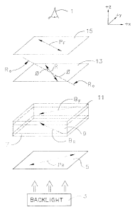
Figure 7 is an exploded schematic view of the
optical components and their respective orientations of
an LCD according to a second embodiment of this
invention. This second embodiment depicted in Figure 7
differs from the first embodiment (Figures 4 - 6) in that
the first embodiment is "X-buffed" and this second
embodiment is "P-buffed". In other words, transmission
axis PR of rear linear polarizes 5 in this embodiment is
substantially parallel to buffing direction BR of rear
orientation film 7, and transmission axis PF of front
polarizes 15 is substantially parallel to buffing
direction BF of front orientation film 11, thus defining a
"P-buffed" display.
As will be appreciated by those of skill in the art,
the display of the first embodiment may be adjusted so as
to be transformed into the LCD of the second embodiment
simply by rotating rear and front polarizers 5 and 15
respectively about 90° each, the rest of the cell such as
LC layer 9, orientation films 7 and 11, retardation film
13, substrates 17 and 19, and electrodes 21 and 23
29
CA 02151291 2004-06-21
remaining substantially the same in both the first and
second embodiments.
Figure 8 is an exploded schematic view of the
optical components and their respective orientations of
an "X-buffed" LCD according to a third embodiment of this
invention. While both the first and third embodiments
illustrated and described herein are "X-buffed", the
principal difference therebetween is the position of
retardation film 13. As shown in Figure 8, retardation
film 13 is disposed rearward or on the backlight side of
liquid crystal layer 9 as opposed to its disposition on
the front side thereof in the first embodiment of this
invention.
A significant advantage associated with the
positioning of retardation film 13 rearward of liquid
crystal layer 9 is the reduction of ambient light
reflection off of the front of the display panel, this
reduction being attributed to fewer mismatching indices
of refraction forward of liquid crystal layer 9 as
discussed in aforesaid Pat. No. 5,594,568.
With respect to the third embodiment shown in Figure
8, optical axis R of retardation film 13 may be rotated
clockwise or counterclockwise relative to direction Ro and
buffing direction BF, counterclockwise rotation causing
the viewing envelope to shift into the upper or positive
vertical region as in the first embodiment and clockwise
rotation causing the envelope to shift into the negative
~I~Z~~I
or lower vertical viewing region. Therefore, if film 13
is disposed on the viewer side of liquid crystal layer 9,
it must be rotated clockwise in order to shift the
viewing envelope into the upper or positive vertical
region, while if retardation film 13 is disposed rearward
of liquid crystal layer 9 as in Figure 8,
counterclockwise rotation of optical axis R relative to
directions Ro and BF as shown in Figure 8 will cause the
viewing envelope to shift into the upper vertical region.
' 10 With respect to the optical components of the third
embodiment, transmission axis PR of rear polarizer 5 is
substantially parallel to direction Ro and buffing
direction BF. Likewise, transmission axis PF of front
polarizer 15 is substantially parallel to buffing
direction BR of rear orientation film 7, buffing
directions BF and BR being substantially perpendicular to
one another. With respect to the retardation value of
retarder 13, each of the first, second, and third
embodiments utilize the aforediscussed retardation
values.
This invention will now be described with respect to
certain examples as follows:
EXAMPLE 1
In this first Example, three separate normally white
a-Si TFT driven twisted nematic AMLCDs were manufactured
and tested for purposes of comparison. The three AMLCDs
31
~~ ~12~I
are referred to in this Example as Display "A", Display
"B", and Display "C" respectively. Each of the three
AMLCDs of this Example utilized the same liquid crystal
layer, RGB color filters, orientation films, electrodes,
and transparent substrates. In other words, Displays "B"
and "C" were constructed simply by adjusting or replacing
the polarizers and/or retardation film 13.
The liquid crystal material of each display had a
birefringence (aN) of about 0.084 at room temperature and
was obtained from E. Merck Ltd. or its United States
representative E.M. Industries, Inc., Hawthorns, New York
as Model No. ZLI-4718. Each of the three displays was
tested at about 35° - 45° C. The electrodes were
conventional in nature and made of transparent ITO, the
substrates were made of glass, and the buffing or
orientation films were conventional in nature and made of
a polyimide material. All three NW AMLCDs of this
Example were of the RGB colored type and had red cell
gaps "d" of about 5.6 wm, and green and blue cell gaps of
about 5.3 wm, each pixel having a triad arrangement of
RGB subpixels. White light emitted from conventional
backlight 3 was utilized in all Examples herein.
The optical construction of Display "A" of this
first Example is shown in Figures 4 - 6. NW Display "A"
included from the rear forward toward viewer 1,
conventional backlight 3, conventional linear polarizer 5
with transmission axis PR, rear transparent glass
32
substrate 17, rear segmented pixel and RGB subpixel
electrodes 21, rear orientation film 7 having buffing
direction BR, liquid crystal layer 9, front orientation
film 11 having buffing direction BF, front electrode 23,
RGB color filters (not shown) corresponding to each
subpixel segment of electrode 21, front transparent glass
substrate 19, uniaxial positively birefringent
retardation film 13 having optical axis R, and finally
front linear polarizer 15 having transmission axis PF.
With respect to Display "A", transmission axis PR of
rear polarizer 5 was substantially parallel to buffing
direction BF of front orientation film 11. Also,
transmission axis PF of front polarizer 15 was
substantially parallel to rear buffing direction BR of
orientation film 7 thus defining an "X-buffed" AMLCD,
buffing directions BF and BR being substantially
perpendicular to one another.
Retardation film 13 was positively birefringent and
had a retardation value of 140 nm. Optical axis R of
retardation film 13 was rotated about 8.5° in the
clockwise direction relative to axis PF and direction BR
so as to define a as shown in Figures 4 - 5 as about
8.5°. Retardation film 13 of Display "A" was obtained
from Nitto Corporation, Japan, or Nitto Denko America,
New Brunswick, New Jersey, as Model No. NRF140.
33
Rear and front linear polarizers 5 and 15 of all
Examples herein were conventional in nature and obtained
from Nitto Denko America, Mc3e1 No. G 1220DUN.
Figure 9 is a contrast ratio contour plot of Display
"A" of this Example when a driving voltage of about 6.8
volts was applied thereto and white light was emitted
from backlight 3. As shown, the high contrast viewing
zone was shifted vertically into the positive vertical
region (above the 0° vertical viewing axis) by the
aforesaid clockwise rotation of optical axis R of
retardation film 13. This display had at least about a
10:1 contrast ratio at +10° vertical over a total range
of about 110° horizontal, this being an improvement of
about 40° with respect to the light valve of prior art
Figure 1 at the same 10° vertical viewing axis. In a
similar manner, Display "A" had at least about a 10:1
contrast ratio at +50° vertical that extended over a
total of about 95° horizontal, this 95° horizontal range
being a signficant improvement over the contrast ratio at
50° vertical with respect to the light valve of Figure 1.
As shown, the viewing zone or envelope of Display
"A" when about 6.8 volts was applied thereto was fairly
uniform (or unskewed) in nature. Additionally, high
contrast ratios (e. g. 50:1) of Display "A" extended over
significantly greater horizontal and vertical expanses
than did their corresponding ratios in the light valve of
prior art Figure 1. For Example, the 50:1 contrast ratio
34
2151291
of Display "A" at +10° vertical extended over a total of
about 80° horizontal as shown in Figure 9, while the
corresponding 50:1 contrast ra~io curve in prior art
Figure 1 at 10° vertical extended only over about 40°
horizontal. Thus, it is evident that the addition of
retardation film 13 with its corresponding retardation
value and optical orientation resulted in a significant
improvement with respect to contrast ratio.
Figure 10 is a contrast ratio contour plot of
Display "A" of this Example when about a 6.0 volt driving
voltage was applied thereto. As shown, the slight
reduction in driving voltage resulted in the contrast
ratio contours slightly shrinking horizontally in the
extreme upper vertical viewing region (e.g. 60°
vertical).
Figure 11 is an intensity (fL) vs driving voltage
plot of Display "A". As shown, Display "A" had
significantly reduced inversion with respect to that of
the prior art light valve shown in Figure 2. This is
evident by the substantial elimination of the prior art
inversion humps present at about 3.0 volts and greater.
No such inversion humps are shown in Figure 11 thus
illustrating the significant improvement over the prior
art with respect to inversion at the illustrated
horizontal viewing angles along the 0° vertical viewing
axis. The elimination of the inversion humps of the
prior art allows Display "A" to be easily and effectively
driven with a plurality of gray level driving voltages
while allowing viewers at different viewing angles to see
substantially the same image with respect to color and
other important viewing characteristics.
Figure 12(a) is a contrast ratio contour plot of NW
a-Si TFT driven "X-buffed" Display "B" of this Example,
Display "B" being manufactured and tested for purposes of
comparison with Display "A". As stated above, Display
"B" was manufactured utilizing the same liquid crystal
material, electrodes, RGB color filters, orientation
films, TFTs, and transparent substrates as Display "A".
The only difference between Display "A" and Display "B"
was that the retardation value of uniaxial positively
birefringent retardation film 13 of Display "B" was about
350 nm instead of the 140 nm value of Display "A" and
optical axis R of retardation film 13 was substantially
parallel to directions Ro and BR. Thus, by comparing the
results of displays "A" and "B", one may easily see the
improvement resulting from the use of a retardation value
in the range of about 100 - 200 nm (e.g. 140 nm) as
opposed to retardation values greater than about 300 nm.
As shown in Figure 12(a) the high contrast viewing
envelope of the 350 nm retardation film Display "B" was
significantly smaller with respect to contrast ratio than
was that of Display "A" shown in Figure 9. By comparing
Figures 9 and 12(a), it is clear that use of the higher
36
2.1~5Z~~1
value retardation film resulted in a smaller viewing
envelope both vertically and horizontally.
Further evident from comparing Figures 9 and 12(a)
is the fact that Display "A" had higher contrast ratios
(e. g. 50:1 and greater) over a larger range of viewing
angles than did Display "B" thus resulting in improved
viewing characteristics. Thus, this additional advantage
associated with the lower value retardation film is
clear.
Figure 12(b) is a contrast ratio contour plot of NW
a-Si TFT driven Display "C" of this Example. Display "C"
differed from Display "A" in that Display "C" was "P-
buffed" as shown in Figure 7 (instead of "X-buffed") and
utilized a uniaxial positively birefringent retardation
film 13 having a retardation value of about 350 nm.
Furthermore, optical axis R of retardation film 13 in
Display "C" was substantially parallel to axis PR and
direction BR (e = about 0°).
All three NW AMLCDs of this Example had their
respective retardation films disposed on the forward or
viewer side of liquid crystal material 9 and sandwiched
between front substrate 19 and front polarizer 15.
Display "C", which is similar to NW displays
described in U.S. Patent No. 5,184,236, had its contrast
ratio contour plot illustrated when about 6.0 volts was
applied thereto in Figure 12(b). As shown in Figure
12(b) as compared to Figure 9, Display "C" had
37
~I ~~ ~~.~
significantly lower contrast ratio expanses both
vertically and horizontally than did Display "A".
Additionally, the extent of higher co:~trast ratios (e. g.
50:1) in Display "A" was greater than that of Display "C"
as is evident by comparing Figure 9 with Figure 12(b).
The orientations of retardation film optical axis R
in Displays "A", "B", and "C", of course, resulted in the
viewing envelopes of Displays "B" and "C" not being
shifted vertically as was the envelope of Display "A".
EXAMPLE 2
A "P-buffed" normally white twisted nematic light
valve was manufactured and tested at about 35° - 40° C in
this Example. This light valve had optical orientations
similar to those shown in Figure 7 and included from the
rear forward toward viewer 1 conventional backlight 3,
rear linear polarizer 5 with transmission axis PR, rear
transparent glass substrate 17, rear continuous electrode
21, rear orientation film 7 with buffing direction BR,
liquid crystal layer 9 having a thickness or cell gap "d"
of about 5.86 ~,m, front orientation film 11 with buffing
direction BF, front continuous electrode 23, front
transparent glass substrate 19, uniaxial positively
birefringent retardation film 13 having a retardation
value of about 120 nm, and finally front linear polarizer
15 having transmission axis PF.
38
~~~1~~I
Retardation film 13 had its optical axis R rotated
clockwise about 20° relative to directions Ro and BR so as
to shift the viewing envelope into the positive vertical
viewing region. In other words, a equaled about 20° as
shown in Figure 7.
Retardation film 13 of this Example was positively
birefringent, uniaxial, and was obtained from Nitto Denko
America, New Brunswick, New Jersey, Model No. NRF120.
The liquid crystal material was identical to the type
utilized in the displays of Example 1, as were the
polyimide orientation films, glass substrates, and
polarizers. Because this Example utilized a light valve,
both electrodes 21 and 23 were continuous in nature as
opposed to the segmented design of the rear electrode of
each AMLCD in Example 1.
Figure 13 is a contrast ratio contour plot of the NW
light valve of Example 2 when about a 5.0 volt driving
voltage was applied thereto. As shown, the 20° clockwise
rotation of optical axis R of retardation film 13
resulted in the shifting of the viewing zone or envelope
into the positive vertical region as is evident by Figure
13. Furthermore, the use of the 120 nm retardation film
resulted in high contrast ratios over a wide range of
horizontal and vertical viewing angles as shown. Thus,
the advantages of such a retardation value and the 20°
rotation of optical axis R are self-evident in view of
the superior viewing characteristics exhibited.
39
Figure 14 is a contrast ratio contour plot of the NW
light valve of this Example when about a 4.0 volt driving
voltage was applied. As shown, the viewing zone remained
in the upper or positive vertical region and was
substantially uniform and unskewed in nature.
An advantage of particular interest associated with
the light valve of this Example is its good contrast at
driving voltages of about 4 - 5 volts. Certain driver
chips often do not allow displays to be driven above 6
volts. In other words, such chips provide for maximum
driving voltages of only about 6 volts, this meaning that
many of the gray level driving voltages are around 4 - 6
volts. Therefore, the superior contrast behavior of this
light valve at such driving voltages is a distinct
advantage. The better behavior of this light valve at
lower driving voltages is clearly an improvement over the
prior art.
EXAMPLE 3
A normally white a-Si TFT driven twisted nematic
AMLCD of the P-buffed type was manufactured and tested at
about 35° - 40° C in this Example. The liquid crystal
material was the same as discussed above in Examples 1
and 2, with this AMLCD having a cell gap "d" of about 5.3
~.m in each of the red, green, and blue subpixels. Each
pixel of this AMLCD included an RGB triad of subpixels.
Unlike the other Examples herein, this AMLCD was driven
2.~5~12~~
with a conventional Gross Tester in that all column and
row address lines were driven together.
As shown generally in Figure 7, the AMT.CD of Example
3 included from the rear forward conventional backlight
3, conventional polarizer 5 having transmission axis PR,
transparent rear glass substrate 17, transparent ITO
segmented subpixel or pixel electrodes 21, rear
orientation film 7 having buffing direction BR, liquid
crystal layer 9 having a RGB cell gap of about 5.3 ~,m,
front orientation film 11 with buffing direction BF, front
continuous electrode 23, red, green, and blue color
filters (not shown) corresponding to each subpixel
electrode segment, front transparent glass substrate 19,
uniaxial positively birefringent retardation film 13
having a retardation value of about 140 nm, and finally
front linear polarizer 15 having transmission axis PF.
Retardation film 13 was again obtained from Nitto
Denko America, New Brunswick, New Jersey, as Model No.
NRF140 and was oriented such that its optical axis R was
rotated clockwise about 5° relative to direction BR and
axis PR. In other words, 8 as shown in Figure 7 was about
5°.
As shown in Figure 15, the AMLCD of this Example had
its viewing zone or envelope shifted into the positive
vertical region by the 5° rotation of retardation film
axis R, the viewing envelope being substantially uniform
in nature as shown.
41
~I ~~ 2~1
This concludes the Examples herein.
As is. evident from the results of the aforesaid
Examples, the provision of a retardation film having a
retardation value of from about 100 - 200 nm (or 100 -
250 nm) on a single side of the liquid crystal layer
significantly improves the viewing characteristics of a
display with respect to both constrast ratio and
inversion. As will be appreciated by those of skill in
the art, the provision of a normally white twisted
l0 nematic LCD having an enlarged and vertically shiftable
viewing zone with reduced inversion is a significant
improvement over conventional normally white LCDs, this
improvement allowing the substantially cheaper to
manufacture NW displays to take the place of more
expensive normally black displays.
Furthermore, the ability to shift the viewing zone
vertically into either the positive or negative vertical
viewing region allows the manufacturer to custom make or
tailor each AMLCD according to the needs of specific
customers. For Example, one customer may require an
AMLCD to be mounted in the lower portion of an avionic
cockpit such that the pilot is forever looking downward
at the display thus requiring the AMLCD to have high
contrast ratios and reduced inversion in the upper or
positive vertical region. In such a case, the desired
viewing characteristics may be achieved simply by
rotation of retardation film 13 as discussed above.
42
~~~Z2~I
Thus, the designs of the different embodiments of this
invention allow different specifications to be realized.
The pre-tilt angle of the displays and light valves
herein may be about 3° in certain embodiments, and the
value of "d/p" (thickness/natural pitch of the liquid
crystal material) of the liquid crystal layers may be set
to about 0.25.
Once given the above disclosure, many other
features, modifications, and improvements will become
apparent to the skilled artisan. Such other features,
modifications, and improvements are, therefore,
considered to be a part of this invention, the scope of
which is to be determined by the following claims:
43