Note: Descriptions are shown in the official language in which they were submitted.
~190933
HIGH PERFORMANCE/LOW COST VIDEO GAME
SYSTEM WITH MULTI-FUNCrIONAL
PERIPHERAL PROCESSING SUBSYSTEM
FIELD OF THE INVENTION
The present invention relates to a high performance low cost video game system.
More particularly, the invention relates to a video game system having a
multifunctional player controller processing subsystem and a flexibly expandable video
game external memory with a low pin out.
BACKGROUND AND SUMMARY OF THE INVENTION
Microprocessor-based home video game systems such as the Nintendo
Entertainment System and the Super Nintendo Entertainment System have been highly
successful in part because they can interactively produce exciting video graphics
involving numerous ~nim~ted moving objects.
The video game system described herein permits game play involving three-
dimensional images having a depth and realism far exceeding these and other
heretofore known video game systems. In the past, computer systems required to
produce such images interactively costs tens of thousands of dollars.
In order to provide such a high performance video game system at a cost
affordable to the average consumer, many features in the video game system were
uniquely optimized. In so doing, many unique features were incorporated into thesystem described herein using novel, multifunctional components having a low pinout,
but which provide for highly flexible future expansion.
~1 9~933
The processor and/or picture processing unit of video game systems such as the
Nintendo Entertainment System and the Super Nintendo Entertainment System
exercise direct control over processing of signals from player input/game control
devices, i.e., player controllers. These prior art systems do not include a player
controller processing subsystem which coacts with the game microprocessor and
picture processing unit to process commands for handling player controller related
input/output.
The present invention is directed in part to a multifunctional peripheral
proces.~in~ subsystem external to the game microprocessor and disclosed coprocessor
which executes commands for handling player controller input/output to thereby lessen
the processing burden on the graphics processing subsystem. The peripheral
processing subsystem is used for both controlling player controller input/outputprocessing and for performing game authenticating security checks continuously
during game play. The peripheral processing subsystem is also used during the game
cartridge/video game system console initial colllmullication protocol using instructions
stored in its boot ROM to enable initial game play.
The peripheral interface is coupled to the coprocessor by a three bit wide serial
bus over which commands are received over one line, clock .sign~l~ over another line
and responses are transmitted to the coprocessor over a third serial line. The peripheral
interface includes a microprocessor for controlling various peripheral interfacefunctions, a read/write random access memory, a boot ROM, a coprocessor command
channel interface, a player controller channel interface, etc., which components interact
to efficiently process player controller commands while also performing other
important functions without requiring significant main processor processing time.
The coprocessor command channel interface responds to coprocessor clock and
command control si~n~ to permit access to the random access memory and to the
-2-
~t 9093~
boot ROM and generates control signals to interrupt the peripheral interface
microprocessor. A peripheral interface macro may be executed to start a read or write
transaction with each peripheral device and thereafter transfer the transaction results
stored in the random access memory to the game microprocessor main memory.
In accordance with another aspect of the present invention, a portable storage
device is used in the form of a game cartridge in the exemplary embodiment having
a low pinout due in part to the use of a multiplexed address/data bus. Memory access
related timing signals are transmitted to the cartridge which may be progr~mm~bly
varied depending upon detected address domain which is used to establish the type of
storage device being used by the video game system.
BRIEF DESCRIPIION OF THE DRAWINGS
These and other features and advantages of the present invention will be better
and more completely understood by referring to the following detailed description of
a presently preferred exemplary embodiment in connection with the dlawillgs, of
which:
Figure 1 is a perspective view of an exemplary embodiment of a video game
system in accordance with the present invention;
Figure 2 is a block diagram of a video game console and game cartridge shown
in Figure l;
Figure 3A is a block diagram of reset related circuitry embodied in the video
game console shown in Figure 2;
Figure 3B depicts timing sign~ generated by the circuitry of Figure 3A;
Figures 4A and 4B is an exemplary, more detailed, implementation of the vide
game console as shown in the Figure 2 block diagram;
Figure 5A shows exemplary ~ign~l~ appearing on the communication channel
between the coprocessor in the peripheral interface subsystem;
~ 9a933
Figure 5B depicts exemplary timing signals for illustrative commands
communicated on this communication channel;
Figures 6A-F show exemplary 3D screen effects achievable using the system
described herein.
Figure 7 is a block diagram of the peripheral interface shown in Figure 2;
Figure 8 depicts in further detail the PIF channel interface shown in Figure 7;
Figure 9A is a block diagram showing in further detail the joystick channel
controller in one of the ports depicted in the block diagram of Figure 7;
Figure 9B is an illustrative representation of data from a player controller
communicated to the peripheral interface 138;
Figures 10A through 10C are flowcharts depicting the sending and receiving
modes of operation for the player controller channel shown in Figure 7;
Figure 11 shows an exemplary player controller with a memory card;
Figure 12 is a block diagram of an exemplary cartridge memory device and
associated accessing circuitry and
Figures 13 and 14 are exemplary timing control and data ~ign~l~ associated with
the memory system depicted in Figure 12.
DETAILED DESCRIPTION OF EXFMPLARY EMBODIMENT
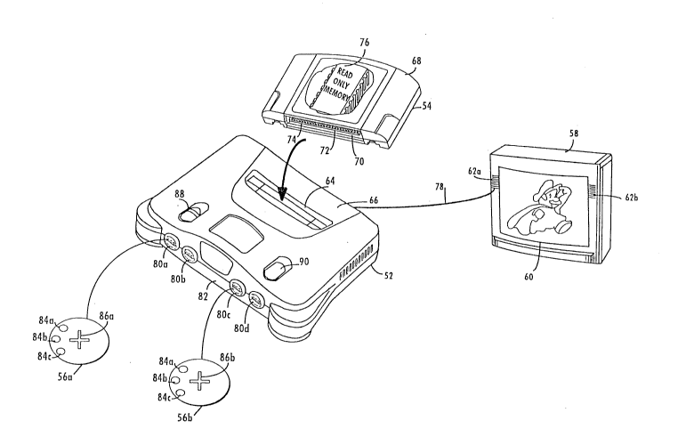
Figure 1 shows an exemplary embodiment of a video game system 50 in
accordance with the present invention. Illustrative video game system 50 includes a
main console 52, a video game storage device 54, and handheld controllers 56a,b (or
other user input devices). Main console 52 is connected to a conventional home color
television set 58. Television set 58 displays 3D video game images on its television
screen 60 and reproduces stereo sound through its speakers 62a,b.
In the illustrative embodiment, the video game storage device 54 is in the form
of a replaceable memory cartridge insertable into a slot 64 on a top surface 66 of
console 52. A wide variety of alternative program storage media are contemplated by
-4-
219~3
the present invention such as CD ROM, floppy disk, etc. In this exemplary
embodiment, video game storage device 54 comprises a plastic housing 68 encasinga printed circuit board 70. Printed circuit board 70 has an edge 72 defining a number
of electrical contacts 74. When the video game storage device 68 is inserted into main
console slot 64, the cartridge electrical contacts 74 mate with corresponding "edge
connector" electrical contacts within the main console. This action electricallyconnects the storage device printed circuit board 72 to the electronics within main
console 52. In this example, at least a "read only memory" chip 76 is disposed on
printed circuit board 70 within storage device housing 68. This "read only memory"
chip 76 stores instructions and other information pert~ining to a particular video game.
The read only memory chip 76 for one game cartridge storage device 54 may, for
example, contain instructions and other information for an adventure game while
another storage device 54 may contain instructions and information to play a car race
game, an educational game, etc. To play one game as opposed to another game, theuser of video game system 50 need only plug the appropriate storage device 54 into
main console slot 64 -- thereby connecting the storage device's read only memory chip
76 (and any other circuitry it may contain) to console 52. This enables a computer
system embodied within console 52 to access the information contained within read
only memory 76, which information controls the console computer system to play the
appropriate video game by displaying images and reproducing sound on color
television set 58 as specified under control of the read only memory game program
information.
To set up the video game system 50 for game play, the user first connects
console 52 to color television set 58 by hooking a cable 78 between the two. Console
52 produces both "video" sign~ls and "audio" signals for controlling color television
set 58. The "video" signals control the images displayed on the television screen 60
and the "audio" signals are played back as sound through television loudspeaker 62.
Depending on the type of color television set 58, it may be necessary to connect a
--s-
2~ 9~3
conventional "RF modulator" between console 52 and color television set 58. This"RF modulator" (not shown) converts the direct video and audio outputs of console 52
into a broadcast type television signal (e.g., for a television channel 2 or 3) that can be
received and processed using the television set's internal "tuner." Other conventional
color television sets 58 have direct video and audio input jacks and therefore don't need
this intermediary RF modulator.
The user then needs to connect console 52 to a power source. This power
source may comprise a conventional AC adapter (not shown) that plugs into a standard
home electrical wall socket and converts the house voltage into a lower voltage DC
signal suitable for powering console 52. The user may then connect up to 4 hand
controllers 56a, 56b to corresponding connectors 80a-80d on main unit front panel 82.
Controllers 56 may take a variety of forms. In this example, the controllers 56a,b
include various function controlling push buttons such as 84a-c and X-Y switches86a,b used, for example, to specify the direction (up, down, left or right) that a player
controllable character displayed on television screen 60 should move. Other controller
possibilities include joysticks, mice pointer controls and a wide range of otherconventional user input devices.
The present system has been designed to accommodate expansion to incorporate
various types of peripheral devices yet to be specified. This is accomplished byincorporating a prog~ ble peripheral device input/output system (to be describedin detail below) which permits device type and status to be specified by programcommands.
In use, a user selects a storage device 54 cont~ining a desired video game, and
inserts that storage device into console slot 64 (thereby electrically connecting read
only memory 76 and other cartridge electronics to the main console electronics). The
user then operates a power switch 88 to turn on the video game system 50 and operates
-6-
2~ ~Uq3s
controllers 86a,b (depending on the particular video game being played, up to four
controllers for four different players can be used with the illustrative console) to
provide inputs to console 52 and thus control video game play. For example,
depressing one of push buttons 84a-c may cause the game to start playing. Movingdirectional switch 86 may cause ~nim~ted characters to move on the television screen
60 in controllably different directions. Depending upon the particular video game
stored within the storage device 54, these various controls 84, 86 on the controller 56
can perform different functions at different times. If the user wants to restart game
play from the beginning, or alternatively with certain game programs reset the game
to a known continuation point, the user can press a reset button 90.
Figure 2 is a block diagram of an illustrative embodiment of console 52 coupled
to a game cartridge 54 and shows a main processor 100, a coprocessor 200, and main
memory 300 which may include an expansion module 302. Main processor 100 is a
computer that executes the video game program within storage device 54. In this
example, the main processor 100 accesses this video game program through the
coprocessor 200 over a communication path 102 between the main processor and thecoprocessor 200, and over another communication path 104a,b between the
coprocessor and the video game storage device 54. Alternatively, the main processor
100 can control the coprocessor 200 to copy the video game program from the video
game storage device 54 into main memory 300 over path 106, and the main processor
100 can then access the video game program in main memory 300 via coprocessor 200
and paths 102, 106. Main processor 100 accepts inputs from game controllers 56
during the execution of the video game program.
Main processor 100 generates, from time to time, lists of instructions for the
coprocessor 200 to perform. Coprocessor 200, in this example, comprises a special
purpose high performance, application specific integrated circuit having an internal
design that is optimized for rapidly processing 3D graphics and digital audio
--7-
~1 ~a~33
information. In the illustrative embodiment, the coprocessor described herein is the
product of a joint venture between Nintendo Company Limited and Silicon Graphics,
Inc. The present invention is not limited to use with the above-identified coprocessor.
Any compatible eoprocessor whieh supports rapid proeessing of 3D graphics and
digital audio may be used herein. In response to instruetion lists provided by main
proeessor 100 over path 102, eoproeessor 200 generates video and audio outputs for
applieation to eolor television set 58 based on data stored within main memory 300
and/or video game storage device 54.
Figure 2 also shows that the audio video outputs of coprocessor 200 are not
provided direetly to television set 58 in this example, but are instead further processed
by external electronics outside of the coprocessor. In particular, in this example,
coproeessor 200 outputs its audio and video information in digital form, but
eonventional home eolor television sets 58 require analog audio and video signals.
Therefore, the digital outputs of eoproeessor 200 must be eonverted into analog form --
a funetion performed for the audio information by DAC and mixer amp 140 and for
the video information by VDAC and eneoder 144. The analog audio signals generated
in DAC 140 are amplified and filtered by an audio amplifier therein that may also mix
audio ~igT~ generated externally of console 52 via the EXTSOUND L/R signal from
connector 154. The analog video signals generated in VDAC 144 are provided to a
video encoder therein which may, for example, convert "RGB" inputs to composite
video outputs compatible with commercial TV sets. The amplified stereo audio output
of the amplifier in ADAC and mixer amp 140 and the composite video output of video
DAC and encoder 144 are provided to directly control home color television set 58.
The composite synchronization signal generated by the video digital to analog
converter in component 144 is coupled to its video encoder and to external connector
154 for use, for example, by an optional light pen or photogun.
71 ~93;~
Figure 2 also shows a clock generator 136 (which, for example, may be
controlled by a crystal 148 shown in Figure 4A) that produces timing signals to time
and synchronize the other console 52 components. Different console components
require dirrerent clocking frequencies, and clock generator 136 provides suitable such
clock frequency outputs (or frequencies from which suitable clock frequencies can be
derived such as by dividing).
In this illustrative embodiment, game controllers 56 are not connected directly
to main processor 100, but instead are connected to console 52 through serial
peripheral interface 138. Serial peripheral interface 138 demultiplexes serial data
~ign~l~ incoming from up to four or five game controllers 56 (e.g., 4 controllers from
serial I/O bus 151 and 1 controller from connector 154) and provides this data in a
predetermined format to main processor 100 via coprocessor 200. Serial peripheral
interface 138 is bidirectional, i.e., it is capable of transmitting serial information
specified by main processor 100 out of front panel connectors 80a-d in addition to
receiving serial information from those front panel connectors. The serial interface
138 receives main memory RDRAM data, clock ~ign~l~, commands and sends
data/responses via a coprocessor serial interface (not shown). I/O commands are
transmitted to the serial interface 138 for execution by its internal processor as will be
described below. In this fashion, the peripheral interface's processor (250 in Figure
7) by handling I/O tasks, reduces the processing burden on main processor 100. As
is described in more detail below in conjunction with Figure 7, serial peripheral
interface 138 also includes a "boot ROM (read only memory)" that stores a small
amount of initial program load (IPL) code. This IPL code stored within the peripheral
interface boot ROM is executed by main processor 100 at time of s~al lu~ and/or reset
to allow the main processor to begin executing game program instructions 108 within
storage device 54. The initial game program instructions 108 may, in turn, control
main processor 100 to initialize the drivers and controllers it needs to access main
memory 300.
_g_
21 9~33
In this exemplary embodiment, serial peripheral interface 138 includes a
processor (see 250 in Figure 7) which, in addition to performing the I/O tasks referred
to above, also co~ -u~icates with an associated security processor 152 within storage
device 54. This pair of security processors (one in the storage device-54, the other in
the console 52) performs, in cooperation with main processor 100, an authentication
function to ensure that only authorized storage devices may be used with video game
console 52.
As shown in Figures 2 and 3A, peripheral interface 138 receives a power-on
reset signal from reset IC 139. Reset IC 139 detects an appropriate threshold voltage
level and thereafter generates a power-on reset signal which, in turn, results in a cold
reset signal being generated by circuit 162, which signal is coupled to the reset input
of main processor 100. In order to ensure that the cold reset signal is generated at the
proper time, a delaying signal CLDCAP is coupled to cold reset signal generatingcircuit 162. Cold reset signal generator 162 includes a Schmidt trigger circuit (which
receives the reset IC signal from reset IC 139) whose output is coupled to one input of
an AND gate. The output of the Schmidt trigger is also coupled to a buffer inverter
whose output and the CLDCAP signal are coupled to a second input of the AND gate.
The output of the AND gate serves as the cold reset signal which is coupled to
rnicroprocessor 250 and main processor 100 and microprocessor 152 shown in Figure
3A. The cold reset signal generated by the cold reset signal generator is fed back to
the input of generator 162 through a diode (not shown). The cold reset signal is also
coupled to the reset input of the processor 250 embodied within the peripheral interface
138 (see Figure 7) and to the reset pin of connector 154 which is coupled to the reset
input of security processor 152. Figure 3B shows the reset IC (RESIC), cold reset
(CLDRES) and CLDCAP signals. Although ~sign~l~ shown in Figures 3B,4A,4B, etc.
are referenced in the specification (and in Figures 2 and 3A) without regard to whether
they are inverted or not (for ease of reference), Figures 3B, 4A and 4B and each of the
-10-
Z19~33
timing diagrams in this disclosure indicate the a~ro~iate inverted nature of the signal
by a line over the signal (or pin) designation as is conventional.
Figure 2 also shows a connector 154 within video game console 52. In this
illustrative embodiment, connector 154 connects, in use, to the electrical contacts 74
at the edge 72 of storage device printed circuit board 70. Thus, connector 154
electrically connects coprocessor 200 to storage device ROM 76. Additionally,
connector 154 connects the storage device security processor 152 to main unit serial
peripheral interface 138. Although connector 154 in the particular example shown in
Figure 2 may be used primarily to read data and instructions from a non-writable read
only memory 76, system 52 is designed so that the connector is bidirectional, i.e., the
main unit can send information to the storage device 54 for storage in random access
memory 77 in addition to reading information from it.
Main memory 300 stores the video game program in the form of CPU
instructions 108. All accesses to main memory 300 are through coprocessor 200 over
path 106. These CPU instructions are typically copied from the game program/data108 stored in storage device 54 and downloaded to RDRAM 300. This architecture
is likewise readily adaptable for use with CD ROM or other bulk media devices.
Although CPU 100 is capable of executing instructions directly out of storage device
ROM 76, the amount of time required to access each instruction from the ROM is
much greater than the time required to access instructions from main memory 300.Therefore, main processor 100 typically copies the game prograrn/data 108 from ROM
76 into main memory 300 on an as-needed basis in blocks, and accesses the main
memory 300 in order to actually execute the instructions. Memory RD RAM 300is
preferably a fast access dynamic RAM capable of achieving 500 Mbytes/second access
times such as the DRAM sold by RAMBUS, Inc. The memory 300 is coupled to
coprocessor 200 via a unified nine bit wide bus 106, the control of which is arbitrated
by coprocessor 200. The memory 300is expandable by merely plll~ing, for example,
~I qas3~
an 8 Mbyte memory card into console 52 via a console memory expansion port (not
shown).
The main processor 100 preferably includes an internal cache memory (not
shown) used to further decrease instruction access time. Storage device 54 also stores
a database of graphics and sound data 112 needed to provide the graphics and sound
of the particular video game. Main processor 100, in general, reads the graphics and
sound data 112 from storage device 54 on an as-needed basis and stores it into main
memory 300 in the form of texture data, sound data and graphics data. In this
example, coprocessor 200 includes a display processor having an internal texturememory into which texture data is copied on an as-needed basis for use by the display
processor.
The storage device 54 also stores coprocessor microcode 156. In this example,
a signal processor within coprocessor 200 executes a computer program in order to
perform its various graphics and audio functions. This computer program, called the
"microcode," is provided by storage device 54. Typically, main processor 100 copies
the microcode 156 into main memory 300 at the time of system startup, and then
controls the signal processor to copy parts of the microcode on an as-needed basis into
an instruction memory within signal processor for execution. Because the microcode
156 is provided by storage device 54, different storage devices can provide different
microcodes -- thereby tailoring the particular functions provided by coprocessor 200
under software control. Because the microcode 156 is typically too large to fit into the
signal processor's internal instruction memory all at once, different microcode pages
or portions may need to be loaded from main memory 300 into the signal processor's
instruction memory as needed. For example, one part of the microcode 156 may be
loaded into signal processor for graphics processing, and another part of microcode
may be loaded for audio processing.
-12-
2~a933
Although not shown in Figure 2, coprocessor 200 also includes a CPU interface,
a serial interface, a parallel peripheral interface, an audio interface, a video interface,
a main memory DRAM controller/interface, a main internal bus and timing control
circuitry. The coprocessor main bus allows each of the various main components
within coprocessor 200 to communicate with one another. The CPU interface is thegateway between main processor 100 and coprocessor 200. Main processor 100 readsdata to and writes data from coprocessor CPU interface via a CPU-to-coprocessor bus.
A coprocessor serial interface provides an interface between the serial peripheral
interface 138 and coprocessor 200, while coprocessor parallel peripheral interface
interfaces with the storage device 54 or other parallel devices connected to connector
154.
A coprocessor audio interface reads information from an audio buffer within
main memory 300 and oul~uL~ it to audio DAC 140. Similarly, a coprocessor video
interface reads information from an RDRAM frame buffer and then oulp~ it to video
DAC 144. A coprocessor DRAM controller/interface is the gateway through which
coprocessor 200 accesses main memory 300. The coprocessor timing circuitry
receives clocking .sign~l~ from clock generator 136 and distributes them (after
appropriate dividing as necessary) to various other circuits within coprocessor 200.
Main processor 100 in this example is a MIPS R4300 RISC microprocessor
designed by MIPS Technologies, Inc., Mountain View, California. For more
information on main processor 100, see, for example, Heinrich, MIPS Microprocessor
R4000 User's Manual (MIPS Technologies, Inc., 1984, Second Ed.).
The conventional R4300 main processor 100 supports six hardware interrupts,
one internal (timer) interrupt, two software interrupts, and one non-m~k~ble interrupt
(NMI). In this example, three of the six hardware interrupt inputs (INTO, INT1 and
INT2) and the non-maskable interrupt (NMI) input allow other portions of system 50
-13-
~1 9~9~3
to interrupt the main processor. Specifically, main processor INTO is connected to
allow coprocessor 200 to interrupt the main processor, the main processor interrupt
INT1 is connected to allow storage device 54 or other external devices to interrupt the
main processor, and main processor interrupts INT2 and NMI are connected to allow
the serial peripheral interface 138 to interrupt the main processor. Any time the
processor is interrupted, it looks at an internal interrupt register to determine the cause
of the interrupt and then may respond in an appropriate manner (e.g., to read a status
register or perform other appropriate action). All but the NMI interrupt input from
serial peripheral interface 138 are ~sk~ble (i.e., the main processor 100 can
selectively enable and disable them under software control).
When the video game reset switch 90 is pressed, a non-m~sk~ble interrupt signal
is generated by peripheral interface circuit 138 and is coupled to main processor 100
as shown in Figure 2. The NMI signal, however, results in non-m~sk~ble, immediate
branching to a predefined initi~li7~tion state. In order to permit the possibility of
responding to reset switch 90 actuation by branching, for example, to the current
highest game level progressed to, the circuit shown in Figure 3A is used. When the
reset switch 90 is depressed, I/O port 164 receives a reset switch input signal which
sets a logic circuit therein and immediately couples an INT2 signal to processor 100.
INT2 is an NMI pre-warning signal and is used to, for example, trigger game processor
100 to save the state of the game in predetermined registers. The logic circuit within
I/O port 164 may be a time delay circuit that ensures that the NMI signal occurs 0.5
second after INT2, as can be seen from the timing sign~ls shown in Figure 3B. The
left hand portion of Figure 3B shows the signal generation when the reset switch is
pushed for less than one-half second. The right hand portion of Figure 3B shows the
timing when the reset switch is pushed for greater than one-half second. Thus, an
individual game program can design~te a desired response to depressing the resetswitch 90 by executing a predefined set of instructions in response to the INT2 signal
before the occurrence of NMI. The CPU 100 also responds to the pre- NMI warning
--14-
93 3
signal INT2 by initiating shut down processing for related audio and video systems and
preparing for its cache memory and other circuits to shut down so that a return is
possible to a desired known state other than merely the beginnin~ of the game. The
NMI signal is also coupled to the peripheral interface microprocessor 250.
In operation, main processor 100 receives inputs from the game controllers 56
and executes the video game program provided by storage device 54 to provide game
processing, ~nim~tion and to assemble graphics and sound commands. The graphics
and sound commands generated by main processor 100 are processed by coprocessor
200. In this example, the coprocessor performs 3D geometry transformation and
lighting processing to generate graphics display commands which the coprocessor then
uses to "draw" polygons for display purposes. As indicated above, coprocessor 200
includes a signal processor and a display processor. 3D geometry transformation and
lighting is performed in this example by the signal processor and polygon rasterization
and texturing is performed by display processor. Display processor writes its output
into a frame buffer in main memory 300. This frame buffer stores a digital
representation of the image to be displayed on the television screen 60. Further~;h~;uilly within coprocessor 200 reads the information contained in the frame buffer
and outputs it to television 58 for display. Meanwhile, the signal processor also
processes sound commands received from main processor 100 using digital audio
signal processing techniques. The signal processor writes its digital audio output into
main memory 300, with the main memory temporarily "buffering" (i.e., storing) the
sound output. Other ~ cuilly in coprocessor 200 reads this buffered sound data from
main memory 300 and converts it into electrical audio signals (stereo, left and right)
for application to and reproduction by television 58.
More specifically, main processor 100 reads a video game program 108 stored
in main memory 300. In response to executing this video game program 108, main
processor 100 creates a list of commands for coprocessor 200. This command list, in
-15-
~ 1 9a~33
general, includes two kinds of commands: graphics commands and audio commands.
Graphics commands control the images coprocessor 200 generates on TV set 58.
Audio commands specifying the sound coprocessor 200 causes to be reproduced on
TV loudspeakers 62. The list of graphics commands may be called- a "display list"
because it controls the images coprocessor 200 displays on the TV screen 60. A list
of audio commands may be called a l'play list" because it controls the sounds that are
played over loudspeaker 62. Generally, main processor 100 specifies both a display
list and a play list for each "frame" of color television set 58 video.
In this example, main processor 100 provides its display/play list to coprocessor
200 by copying it into main memory 300. Main processor also arranges for the main
memory 300 to contain a graphics and audio database that includes all that the data
coprocessor 200 needs to generate graphics and audio requested in the display/play list
110. For example, main processor 100 may copy the appropriate graphics and audiodata from storage device read only memory 76 into the graphics and audio database
within main memory 300. Main processor 100 tells coprocessor 200 where to find the
display/play list it has written into main memory 300, and that display/play list may
specify which portions of graphics and audio database the coprocessor 200 should use.
The coprocessor's signal processor reads the display/play list from main
memory 100 and processes this list (accessing additional data within the graphics and
audio database as needed). The signal processor generates two main outputs: graphics
display commands for further processing by display processor; and audio output data
for temporary storage within main memory 300. Once signal processor writes the
audio output data into main memory 300, another part of the coprocessor 200 called
an "audio interface" (not shown) reads this audio data and outputs it for reproduction
by television loudspeaker 62.
-16-
~ 1 9~9~3
The signal processor can provide the graphics display commands directly to
display processor over a path internal to coprocessor 200, or it may write thosegraphics display commands into main memory 300 for retrieval from the main memory
by the display processor. These graphics display commands command display
processor to draw ("render") specified geometric images on television screen 60. For
example, display processor can draw lines, triangles or rectangles based on these
graphics display commands, and may fill triangles and rectangles with particulartextures (e.g., images of leaves of a tree or bricks of a brick wall such as shown in the
exemplary screen displays in Figures 6A through ~i~ stored within main memory 300 --
all as specified by the graphics display command. It is also possible for main
processor 100 to write graphics display commands directly into main memory 300 so
as to directly command the display processor. The coprocessor display processor
generates, as output, a digitized representation of the image that is to appear on
television screen 60.
This digitized image, sometimes called a "bit map," is stored (along with "depthor Z" information) within a frame buffer residing in main memory 300 of each video
frame displayed by color television set 58. Another part of coprocessor 200 called the
"video interface" (not shown) reads the frame buffer and converts its contents into
video signals for application to color television set 58.
Each of Figures 6A-6F was generated using a three-dimensional model of a
"world" that represents a castle on a hilltop. This model is made up of geometric
shapes (i.e., lines, triangles, rectangles) and "textures" (digitally stored pictures) that
are "mapped" onto the surfaces defined by the geometric shapes.. System 50 sizes,
rotates and moves these geometric shapes appropriately, "projects" them, and puts
them all together to provide a realistic image of the three-dimensional world from any
arbitrary viewpoint. System S0 can do this interactively in real time response to a
person's operation of game controllers 86.
-17-
~1 9~933
Figures 6A-6C and 6F show aerial views of the castle from four different
viewpoints. Notice that each of the views is in perspective. System 50 can generate
these views (and views in between) interactively with little or no discernible delay so
it appears as if the video game player is actually flying over the castle.
Figures 6D and 6E show views from the ground looking up at or near the castle
main gate. System 50 can generate these views interactively in real time response to
game controller inputs commanding the viewpoint to "land" in front of the castle, and
command,ing the "virtual viewer" (i.e., the im~,~in~ry person moving through the 3-D
world through whose eyes the scenes are displayed) to face in different directions.
Figure 6D shows an example of "texture mapping" in which a texture (picture) of a
brick wall is mapped onto the castle walls to create a very realistic image.
Figure 4A and 4B comprise an exemplary more detailed implementation of the
Figure 2 block diagram. Components in Figures 4A and 4B, which are identical to
those represented in Figure 2, are associated with identical numerical labels. Many of
the components shown in Figures 4A and 4B have already been described in
conjunction with Figure 2 and further discussion of these components is not necessary.
Figures 4A and 4B show the interface between system components and the
specific ~ign~l~ received on device pins in greater detail than shown in Figure 2. To
the extent that voltage levels are indicated in Figures 4A and 4B, VDD represents +3.3
volts and VCC represents +5 volts.
Focusing first on peripheral interface 138 in Figure 4B, ~i~?n~l~ such as
CLDRES, NMI, RESIC, CLDCAP and RSWIN have been previously explained in
conjunction with Figures 2, 3A and 3B which explanation will not be repeated herein.
Three coprocessor 200/peripheral interface 138 communication signals are shown:
-18-
21~33
PCHCLK, PCHCMD, and PCHRSP. These signals are transmitted on 3 bit wideperipheral interface channel bus as shown in Figures 2, 4A and 4B. The clock signal
PCHCLK is used for timing purposes to trigger sampling of peripheral interface data
and commands. The clock signal is transmitted from the coprocessor 200 to the
peripheral interface 138.
Coprocessor 200 and CPU 100, based on the video game program store in
storage device 54, supply commands for the peripheral interface 138 to perform on the
PCHCMD control line. The command includes a start bit ~leld, a command code field
and data or other information.
The peripheral interface circuitry (as will be described further below) decodes
the command and, if the data is ready in response to the command, sends a PCHRSPresponse signal comprising an acknowledge signal "ACK" followed by the response
data. Approxim~tely two clock pulses after the peripheral interface 138 generates the
acknowledgment signal ACK, data tr~n~mi~sion begins. Data received from the
peripheral interface 138 may be information/instructions stored in the boot ROM or
controller status or controller data, etc.
Figure 5A shows representative signals transmitted across the PCHCLK,
PCHCMD and PCHRSP lines. The relationships between the clock signal and the
peripheral interface sampling of the PCHCMD line and the clock signal and the
peripheral interface ouLpu~ling of the response is shown in Figure 5A. Additionally,
the relationships between the clock signal and coprocessor 200 (RCP) outputting a
PCHCMD and the coprocessor sampling the PCHRSP is shown in Figure 5A. As
suggested by Figure 5A, the high and low levels of the clock signal may have different
pulse widths dependent upon whether the system is to be lltili~e-l with NTSC or PAL.
Figure 5B shows exemplary ~ign~l~ appearing on the peripheral interface channel for
four exemplary commands serving to read 4 bytes into memory, write 4 bytes into
-19--
21 9~9~
memory, execute a peripheral interface macro instruction or write 64 bytes into
peripheral interface buffer memory. Further explanation of the peripheral interface
device and these commands will be described in detail below.
Turning back to the Figure 4B peripheral interface 138, SECCLK, SECTRC and
SECTRD are three security related signals coupled between two security processors
embodied within the peripheral interface 138 and game cartridge, respectively.
SECCLK is a clock signal used to clock security processor operations in both theperipheral interface and the game cartridge. SECTRC is a signal sent from the
peripheral interface 138 to the game cartridge defining a data tr~ncmi~sion clock signal
window in which data is valid and SECTRD is a data tr~n~mi.~ion bus signal in which
data from the peripheral interface 138 and data from the game cartridge securityprocessor are exchanged at times identified by the SECTRD tr~n~mi.c.~ion clock pulses.
Finally, the peripheral interface 138 includes a pin RSWIN which is the reset switch
input pin.
Turning next to connector 154, as previously mentioned, the system 50 includes-
an expansion capability for ~lcling another controller 56. Data from such a controller
would be transmitted via the EXTJOY I/O pin of the connector 154. The three above-
mentioned security related signals are coupled between the game cartridge security
processor and peripheral interface processor at the pins labeled SECTRD, SECTRC
and SECCLK.
The cartridge connector additionally couples a cold reset signal CRESET to the
game cartridge security processor to enable a power on reset function. Additionally,
if during processor authentication checking, if, for example, the peripheral interface
processor does not receive data which matches what is expected, the cartridge
processor may be placed in a reset state via the CRESET control pin.
-20-
219~933
The NMI input is a control pin for coupling an NMI interrupt signal to the
cartridge. The control line CARTINT is provided to permit an interrupt signal to be
generated from the cartridge to CPU 100 to, for example, if devices are coupled to the
cartridge requiring service by CPU 100. By way of example only, a buL~ storage
device such as a CD ROM is one possible device requiring CPU interrupt service.
As shown in Figure 4B, the system bus is coupled to the cartridge connector 154
to permit accessing of program instructions and data from the game cartridge ROMand/or bulk storage devices such as CD ROM, etc. In contrast with prior video game
systems such as the Nintendo NES and SNES, address and data signals are not
separately coupled on dirrerellt buses to the game cartridge but rather are multiplexed
on an address/data 16 bit wide bus. Read and write control signals and address latch
enable high and low signals, ALEH and ALEL, respectively are also coupled to thegame cartridge. The state of the ALEH and ALEL ~ign~ defines the significance ofthe information transmitted on the 16 bit bus. The read signal RD is a read strobe
signal enabling data to be read from the mask ROM or RAM in the game cartridge.
The write signal WR is a strobe signal enabling the writing of data from the
coprocessor 200 to the cartridge static RAM or bulk media device. The multiplexed
use of the 16 bit address/data bus is described in further detail in conjunction with
Figures 12-14 in describing external memory accessing.
Sound may be output from the cartridge and/or through connector 154 to the
audio mixer 142 channel 1 and channel 2 inputs, CHlEXT and CH2EXT, respectively.The external sound inputs from SOUNDL and SOUNDR will be mixed with the sound
output from the coprocessor via the audio DAC 140 and the CHlIN, CH2IN inputs tothereafter output the combined sound signal via the audio mixer outputs CHlOUT,
CH20UT which are, in turn, coupled to the AUDIOL and AUDIOR inputs of the
audio video output connector 149 and thereafter coupled to the TV speakers 62a,b.
--21 -
~9~933
The connector 154 also receives a composite sync signal CSYNC which is the
output of video DAC 144 which is likewise coupled to the audio video output
connector 149. The composite sync signal CSYNC, as previously described, is utilized
as a synchronization signal for use in synchroni~ing, for example,- a light pen or
photogun.
The cartridge connector also includes pins for receiving power supply and
ground ~sign~l~ as shown in Figures 4B. The +3.3 volts drives, for example, the 16 bit
AD bus as well as other cartridge devices. The 12 volt power supply connection is
utilized for driving bulk media devices.
Turning to coprocessor 200 in Figure 4A, many of the ~ign~l~ received or
transmitted by coprocessor 200 have already been described, which will not be
repeated herein. The coprocessor 200 outputs an audio signal indicating whether audio
data is for the left or right channel, i.e., AUDLRCLK. Serial audio data is output on
a AUDDATA pin. Timing for the serially transmitted data is provided at the
AUDCLK pin. Coprocessor 200 outputs seven video ~ign~l~ SRGBO through SRGB7
which synchronized RGB digital signals are coupled to video DAC 144 for conversion
to analog. Coprocessor 200 generates a timing signal SYNC that controls the timing
for the SRGB data which is coupled to the TSYNC input of video DAC 144.
Coprocessor 200 receives a video clock input from clock generator 136 via the VCLK
input pin for controlling the SRGB signal timing. The coprocessor 200 and CPU 100
use a PVALID SIGNAL to indicate that the processor 100 is driving a valid command
or data identifier or valid address/data on the system bus and an EVALID signal to
indicate that the coprocessor 200 is driving a valid command or data identifier or valid
address/data on the system bus. Coprocessor 200 supplies CPU 100 with master clock
pulses for timing operations within the CPU 100. Coprocessor 200 and CPU 100
additionally use an EOK signal for indicating that the coprocessor 200is capable of
accepting a processor 100 command.
-22--
2 1 ~ 3
Turning to main memory RDRAM 300, 302, as depicted in Figure 4A, two
RDRAM chips 300a and 300b are shown with an expansion RDRAM module 302.
As previously described, the main memory RDRAM may be expanded by plu~ing in
a memory module into a memory expansion port in the video console housing. Each
RDRAM module 300a,b, 302 is coupled to coprocessor 200 in the same manner.
Upon power-up RDRAM 1 (300a) is first initialized, then RDRAM2 (300b) and
RDRAM3 (302) are initialized. RDRAM 1 is recognized by coprocessor 200 since itsSIN input is tied to VDD, as shown in Figure 4A. When RD1 is initialized under
software control SOUT will be at a high level. The SOUT high level signal is coupled
to SIN of RDRAM 2 (300b) which operates to initialize RDRAM2. SOUT will then
go to a high level which operates to initialize RDRAM3 (302) (if present in the
system).
Each of the RDRAM modules receives bus control and bus enable sign~l~ from
coprocessor 200. The coprocessor 200 outputs a TXCLK signal when data is to be
output to one of RDRAM1 through 3 and a clock signal RXCLK is output when data
is to be read out from one of the RDRAM banks. The serial in (SIN) and serial out
(SOUI~ pins are used during initi~li7~tion, as previously described. RDRAM receives
clock signals from the clock generator 136 output pin FSO.
Clock generator 136 is a three frequency clock signal generator. By way of
example, the oscillator within clock generator 136 may be a phase-locked locked loop
based oscillator which generates an FSO signal of approxim~tely 250MHz. The
oscillator also outputs a divided version of the FSO signal, e.g., FSO/5 which may be
at approxim~tely 50 MHz, which is used for timing operations involving the
coprocessor 200 and video DAC 144, as is indicated in Figures 4A and 4B. The FSCsignal is utilized for timing the video encoder carrier signal. Clock generator 136 also
includes a frequency select input in which frequencies may be selected depending upon
whether an NTSC or PAL version of the described exemplary embodiment is used.
-23-
~l9~33
Although the FSEL select signal is contemplated to be utilized for configuring the
oscillator for NTSC or PAL use, as shown in Figure 4A, the input resets the oscillator
under power-on reset conditions. When connected to the power on reset, the oscillator
reset is released when a predetermined threshold voltage is reached. -
Figure 7 is a block diagram of peripheral interface 138 shown in Figure 2. Theportion of peripheral interface 138 previously described in conjunction with Figures
3A and 3B is not shown in Figure 7. Peripheral interface 138 is utilized for I/Oprocessing, e.g., controlling the game controller 56 input/output processing, and for
performing game authenticating security checks continuously during game play.
Additionally, peripheral interface 138 is utilized during the game cartridge/coprocessor
200 communication protocol using instructions stored in boot ROM 262 to enable
initial game play. Peripheral interface 138 includes CPU 250, which may, for
example, be a 4 bit microprocessor of the type manufactured by Sharp Corporation.
CPU 250 executes its security program out of program ROM 252. As previously
described, the peripheral interface processor 250 communicates with the securityprocessor 152 embodied on the game cartridge lltili7ing the SECTRC, SECTRD and
SECCLK ~ign~l~. Peripheral interface port 254 includes two 1 bit registers for
temporarily storing the SECTRC and SECTRD signals.
Overall system security for authenticating game software is controlled by the
interaction of main processor 100, peripheral interface processor 250, boot ROM 262
and cartridge security processor 152. Boot ROM 262 stores a set of instructions
executed by processor 100 shortly after power is turned on (and, if desired, upon the
depression of reset switch 90). The boot ROM program includes instructions for
initi~ ing the CPU 100 and coprocessor 200 via a set of initial program loading
instructions (IPL). Authentication calculations are thereafter performed by the main
processor 100 and the result is returned to the CPU 250 in peripheral interface 138 for
verification. If there is verification, the game program is transferred to the RDRAM,
--24--
2~ 9~933
after it has been initialized, and a further authentication check is made. Upon
verification of an authentic game program, control jumps to the game program in
RDRAM for execution. Continuous authentication calculations continue during gameplay by the authenticating processor in the peripheral interface 138 and by security
processor 152 such as is described, for example, in U.S. Patent 4,799,635 and related
U.S. Patent 5,426,762 which patents are incorporated by reference herein.
Turning back to Figure 7, a PCHCLK clock signal having a frequency of, for
example, approxim~tely 15MHz is input to clock generator 256 which, in turn,
supplies an approximately lMHz clocking signal to CPU 250 and an approxim~tely
lMHz clock signal along the line SECCLK for tr~n.~mi.ssion to the game cartridgesecurity processor 152. PIF channel interface 260 responds to PCHCLK and
PCHCMD control signals to permit access of the boot ROM 262 and RAM 264 and
to generate signals for controlling the interruption of CPU 250, when appropriate.
Figure 8 is a block diagram of the PIF channel interface 260 shown in Figure 7.
As shown in Figure 8, commands are serially loaded into shift register 282 on line
PCHCMD under the control of clock pulses PCHCLK. Shift register 282 operates as
a serial to parallel converter and a parallel to serial converter as explained below.
Controller 284 decodes comm~ncl~ which are output in parallel from shift register 282
to, for example, generate read or write control signals for accessing information from
RAM 264, reading instructions out of boot ROM 262 or to generate interrupt control
~ign~l~ to be communicated to CPU 250 and/or generates other conventional control
signals (CTL) as needed. Information accessed from RAM 264 and instructions
accessed from boot ROM 262 are loaded via internal bus 285 in parallel to shift
register 282 and then are clocked out of shift register 282 serially on the response line
PCHRSP. If the command loaded into shift register 282 is a write to RAM 264
command, controller 284 will decode the command, generate a write control signal and
output data associated with the command in parallel from the shift register to RAM
-25 -
2 1 9~93~
264. Thus, controller 284 exercises DMA control in controlling accessing of RAM
264 and boot ROM 262 data, and loading such data in shift register 282 and in
controlling data transfer from shift register 282 to RAM 264. PIF channel interface
260 also includes a buffer control/status register 283 for storing channel status and/or
control bits which may be accessed by controller 284 or CPU 250. This register stores
information indicative of current buffer 264 access size and buffer 264 read/write
status.
As shown in Figure SA, the PCHCLK signal is the basic clock signal which
may, for example, be a 15.2 MHz signal utilized for clocking communication
operations between the coprocessor 200 and the peripheral interface 138. Figure SA
also shows the timing for the PCHCMD command issued by the coprocessor 200 to
the peripheral interface 138. The command is utilized for reading and writing from
and to RAM 264 and for reading from boot ROM 262. The peripheral interface 138
in turn provides a PCHRSP response which includes both accessed data and an
acknowledgment signal. The lower three timing signals shown in Figure SA are
sign~ls from the perspective of the peripheral interface (PIF) whereas the upper three
timing signals are from the perspective of the coprocessor.
In the present exemplary embodiment, four commands are contemplated
including a read 4 byte from memory command for reading from RAM 264 and boot
ROM 262, a write 4 byte memory command for writing to RAM 264, a PIF macro
command for reading 64 bytes from buffer 264 and accessing controVdata from the
player controller (hereinafter JoyChannel). The CPU 250 is triggered to send or
receive JoyChannel data by the PIF macro instruction. The main processor 100 maythus generate a PIF macro command which will initiate UO processing operations by
CPU 250 to lessen the processing burden on main processor 100. The main processor
100 may also issue a write 64 byte buffer command which writes 64 bytes into RAM264.
--26-
~ 90~33
Turning back to Figure 7, peripheral interface 138 also includes a bus arbitrator
258 which allocates access to RAM 264 between CPU 250 and PIF channel interface
260. RAM 264 operates as a working RAM for CPU 250 and stores cartridge
authenticating related calculations. RAM 264 additionally stores status data such as,
for example, indicating whether the reset switch has been depressed. RAM 264 also
stores controller related information in, for example, a 64 byte buffer within RAM 264.
Figure 5B shows exemplary command formats for reading and writing from and to the
64 byte buffer.
Both the buffer RAM 264 and the boot ROM 262 are in the address space of
main processor 100. The CPU 250 of the peripheral interface 138 also can access
buffer RAM 264 in its address space. Memory protection techniques are utilized in
order to prevent inappropriate access to portions of RAM 264 which are used for
authenticating calculations.
As can be seen in Figure 7, the reset and interrupt related signals shown in
Figures 3A and 3B, such as CLDRES, CLDCAP and RESIC are generated and/or
processed as explained above. The signal RSWIN is coupled to port 268 upon the
depression of reset switch 90 and, as explained above, the NMI and the pre-NMI
warning signal, INT2, are generated as previously described in conjunction with Figure
3B.
Port 268 includes a reset control register storing bits indicating whether an NMI
or INT2 signal is to be generated. A third bit in the reset control register indicates
whether the reset switch 90 has been depressed.
As mentioned previously, peripheral interface 138, in addition to its other
functions, serves to provide input/output processing for two or more player controllers.
As shown in Figure 1, an exemplary embodiment of the present invention includes four
--27-
2 1 90933
sockets 80a-d to accept up to four peripheral devices. Additionally, the presentinvention provides for including one or more additional peripheral devices. See
connector 154 and pin EXTJOY I/O. The 64 byte main processor 100 does not
directly control peripheral devices such as joystick or cross-switch based controllers.
Instead, main processor 100 controls the player controllers indirectly by sending
commands via coprocessor 200 to peripheral interface 138 which handles I/O
processing for the main processor 100. As shown in Figure 7, peripheral interface 138
also receives inputs from, for example, five player controller channels via channel
selector 280, demodulator 278, joystick channel controller 272 and port 266. Joystick
channel data may be transmitted to peripheral devices via port 266 to joystick channel
controller 272, modulator 274 and channel select 276.
With respect to JoyChannel communication protocol, there is a command
protocol and a response protocol. After a command frame, there is a completion signal
generated. A response frame always comes after a command frame. In a response
frame, there is a completion signal generated after the response is complete. Data is
also sent from the peripheral interface 138 to the JoyChannel controllers. The CPU
250 of the peripheral interface controls such communications.
Each channel coupled to a player controller is a serial bilateral bus which may
be selected via the channel selector 276 to couple information to one of the peripheral
devices under the control of the four bit CPU 250. If the main processor 100 wants to
read or write data from or to player controllers or other peripheral devices, it has to
access RAM 264. There are several modes for accessing RAM 264 as shown in Figure5B. The 64 bit CPU 100 may execute a 32 bit word read or write instruction from or
to the peripheral interface RAM 264. Alternatively, the CPU may execute a write 64
byte DMA instruction. This instruction is performed by first writing a DMA starting
address into the main R~M address register. Thereafter, a buffer RAM 264 addresscode is written into a predetermined register to trigger a 64 byte DMA write operation
--28--
21 ~33
to transfer data from a main RAM address register to a fixed destination address in
RAM 264.
A PIF macro also may be executed. A PIF macro involves an exchange of data
between the peripheral interface RAM 264 and the peripheral devices and the re~-ling
of 64 bytes by DMA. By using the PIF macro, any peripheral device's status may be
determined. The macro is initiated by first setting the peripheral interface 138 to
assign each peripheral device by using a write 64 byte DMA operation or a write 4
byte operation (which could be skipped if done before and no change in assignment
is needed). Thereafter, the DMA destination address is written onto a main RAM
address register and a predetermined RAM 264 address code is written in a PIF macro
register located in the coprocessor which triggers the PIF macro. The PIF macro
involves two phases where first, the peripheral interface 138 starts a reading or writing
transaction with each peripheral device at each assigned mode which results in updated
information being stored in the peripheral interface RAM 264. Thereafter, a read 64
byte DMA operation is performed for transferring 64 bytes from the fixed DMA
starting address of the RAM 264 to the main RAM address register progr~mm~ble
DMA destination address within main RAM 300. See Figure 5B for PIF macro timing
Si~l~l.S.
The table below exemplifies the manner in which the 64 bit main processor 100
comlllullicates using its memory address space by addressing RAM 264 to exchangeinformation with the JoyChannels.
--29--
21 ~3~
OxlFC007FC l l ¦ Format
OXlfc007F8
_
~ Ch. 6 Nth R~ Data~
~ Ch. 5 Nth Rx Data Ch. 6 Tx Size Area Ch. 6 Rx Size Area Ch. 61st Tx
~_ ~_ ~
Ch. 3, Ch. 4, Ch. 5
~ Ch. 1 Nth Rx Data ¦ Ch. 2 Rx Size Area ¦ Ch. 2 Rx SizeArea ¦ Ch. 21st Tx
I M l~vtes I N Bvtes l Dat~a
~ Ch. 1 Mth Tx Data I Ch. 1st Rx Data
OxlFC007C4
OxlFC007COCh.l Tx Size Area Ch. 1 Rx Size Area Ch. 1 1st Tx Data <~
~_ ~i_
Addr. +0 Addr. +1 Addr. +2 Addr. +3
-30-
2i9~933
There are six JoyChannels available in the present exemplary embodiment.
Each Channel's transmit data and receive data byte sizes are all independently
~ign~hle by setting size parameters. In the exemplary embodiment, all six channels
size parameter setups are required, whether they are used or not. As shown above,
RAM 264 is to be used for each channel's TxData/RxData assignment.
TxData/RxData ~.signment becomes effective when main processor 100 sets a formatflag (Ox1FC007FC bO) by using Wr64B or Wr4B.
In the exemplary embodiment, if processor 100 writes "OxOO", "OxFD", "OxFE"
or "OxFF" as TxData Size, the data is not recognized as TxData size but has a special
function as indicated below. They become effective when processor 100 sets format
bit (Ox1FC007FC bO) by using Wr64B or Wr4B.
"OxOO" = Channel Skip
If OxOO is written as TxData Size, respective JoyChannel transaction is not
executed.
"OxFD" = Channel Reset
If OxFD is written as TxData Size, PIF outputs reset signal to respective
JoyChannel.
"OxFE" = Format End
If OxFE is written as TxData Size, TxData/RxData ~ignment is end at this
")xFE". In other words, the TxData Size or RxData Size after "OxFE" is
ignored.
"OxFF" = Dummy Data
TxData Size's OxFF is used as the dummy data for word ~lignin~
the data area.
-31 -
2 1 ~33
Each Channel has four flags. Two of them have information from processor 100
to JoyChannel and others from JoyChannel to processor 100.
Skip = Channel Skip
If processor 100 sets this flag to "1", respective JoyChannel
transaction is not executed. This flag becomes effective without
formal flag.
Res = Channel Reset
If 64 bit CPU set this flag to "1", PIF outputs reset signal to
respective JoyChannel. This flag becomes effective without
format flag.
NR = No Response to JoyChannel
When each JoyChannel's peripheral device does not respond, the
respective NR bit is set to "1". This is the way to detect the number of currently
connected peripheral devices.
Err = JoyChannel Error
When communication error has occurred between PIF and
peripheral device, Err flag is set to "1".
If the 64 bit CPU 100 wants to change JoyChannel's Tx/RxData assignment, a
32 bit format flag is used, where a certain bit(s) specify the desired format. For
example, when Wr64B or Wr4B is issued when this flag is "1", PIF executes each
JoyChannel's Tx/RxData assignment based on each channel's Tx/Rx Size. In other
words, unless this flag is set to "1" with Wr64B or Wr4B, Tx/RxData area ~.~SigT ment
does not change. After Tx/RxData assignment, this flag is reset to "O" automatically.
-32-
219~933
Figure 9A is a block diagram of the joystick channel controller 272 and port 266shown in Figure 7. As indicated in Figure 9A, bus 287 which is coupled to CPU 250
couples data to be transmitted to JoyChannel through port register 290 to FIFO buffer
312. Under the control of controller 310, four bit data is then loaded into shift register
314 in parallel and serially clocked out to modulator 274 into an identified JoyChannel
selected by channel select 276 based on an address resident in address register RA299.
Data received from a JoyChannel is input via channel selector 280 to demodulator 278
and then is serially loaded into shift register 314. The serial data is converted to
parallel by shift register 314, loaded into FIFO 312 and then coupled to CPU 250 via
register 292. Controller 310 generates conventional control signals (CTL) used to
control the data exchange described herein.
The function of the various port 266 registers are sllmm~rized below. Register
RO(290) is a JoyChannel output register for receiving data to be output via modulator
274 and channel select 276. Joystick Channel controller 272 uses a JoyChannel
address register RA to control the channel select to identify particular JoyChannels for
input and output of data. Register R1 292 is a four bit JoyChannel input data register.
Register CR 294 is a JoyChannel control register which, for example, identifies
whether data is being received or transmitted. Register SR 296 is a JoyChannel status
register which, for example, includes a bit indicating that a Joy Bus data register is
ready and that a bit indicating that a Joy Bus error has been detected. Register ER 298
is a Joy Bus error register that indicates whether there has been a collision error, frame
error, overrun error or no response error. With respect to the no response signal, even
if a controller is not connected and therefore could not give a response, the lack of
response is treated as an error signal in the exemplary embodiment of the present
invenhon.
As can be seen in Figure 9A, controller 310 supplies the status register and theerror register with the status and error information identified above in parallel and
-33--
21~933
receives control signals from control register 294 for controlling buffer 312 and shift
register 314 to respond according to the current mode of operation.
The video game system is proglanlllled to allow one to four players to play at
the same time by, for example, setting up RDRAM 300 as shown below:
-34-
21~933
PIfRAM Format Flag On
Addr. +60 ~ I I I n x n
Ch.S Ch.6
0\00 _'
Channel Skip _ = ~
~ Ch. 4
O~F~ ~:GZ~
0 x FF = Ch. 3
Addr. +8 n ,~ FF _ ~ Ch. 2
Addr. +4 T ~
DMA Start Addr. n x FF ~ Ch. 1
Addr. +0 Addr. +1Addr/ +2 Addr. +3
Ch.1-4 Ch.1~4 Ch.1~4
TxData Size RxData Size Read Controller
1 Byte 4 Byte Data Command
OxOl
-35-
21~9~3
Thereafter, the DMA start address is written in a RDRAM coprocessor 200
address register. A RAM 264 address code is then written into the write 64 byte
register in the coprocessor 200 and a write DMA destination address is written in the
RDRAM address register in the coprocessor. Thereafter, the address in the 64 byte
RAM 264 is written in the PIF macro register in the coprocessor.
The controllers response is returned to RDRAM. If only two controllers are
connected to channel 1 and channel 2, DMA destination RAM area resulting thelerlo
after the PIF macro is executed is preferably as shown below. However, if a controller
is connected to channel 3 or channel 4, the channel's RAM area changes to the same
as channel 1 or channel 2.
--36-
~1 9~33
PIfRAM Format Flag is Reset to "0"
Addr. +60 ~ I I rn x (~û
Ch.5 Ch.6
0~00 ~
~5ii~ Channel Skin ~ ,
No Response from JoyChannel T
0 x FF0 x û1 1 0 x ~4 1Ox 01 I Ch. 4
No Resnonse fron~ JovChannel I ¦
O x FF O x 01 O x 84 O x 01 Ch. 3
No Resnonse
BAG ST t l -0 n T . R F. n c FJovstick X Pole Jovstick Y Pole
Addr. +8 0 x FF 0 x 01 0 x 04 0 x 01 Ch. 2
Addr. +4 BAG ST t 1 ~0 (1 T R F n c FJovstick X PoleJovstick Y Pnle
DMA Destination O x FF o x 01 O x 04 O x 01 Ch. 1
Addr. +0 Addr. +1 Addr. +2 Addr. +3
211 9C9~3
The peripheral device channel is designed to accept various types of future
peripheral devices. The present exemplary embodiment uses an extensible command
which is to be interpreted by peripherals including future devices. The commandsoccupy the first byte of a TxData area in RAM 264. Many bits and commands are
reserved for future extension. Exemplary commands relating to peripheral devices are
shown below. Commands are also provided for read and writing data to a memory
card. Backup data for a game may be stored on a memory card. In this fashion, nobackup battery need be used for this memory during game play since it plugs into the
controller. Certain of these commands contemplate an expansion memory card module
313 that plugs into a player controller 56 as is shown in Figure 11. For further details
relating to exemplary controllers that may be used in system 50 and the
communications protocol between such controller and the peripheral interface 138 (and
processing associated thelewilll) reference is made to Japanese patent application no.
00534 filed on October 9, 1995 n~ming Nishiumi et al as inventors, which application
is incorporated herein by reference. Exemplary controller commands are shown
below.
Command 0: Ask each peripheral device's type and status flag
TxSize: 1 byte RxSize: 3byte
This comm~nd is used to ask the peripheral device's type and status flags, and
its answer is supposed to be returned into RX data area.
--38-
21 90933
b7 ¦ b6 ¦ bS ¦ b4 ¦ b3 ¦ b2 ¦ b I ¦ bO
TxData 1 BYTE ~ Command O -
1 BYTE ~ Type L
RxData 2 BYTE ~ Type H
3 BYTE ~ Status Flag
Peripheral Device's Type
This type is provided from the connected peripheral device about its functions
and features as shown for example below.
b7 b6 b5 b4 b3 b2 bl bO
H Reserved Reserved Reserved Reserved Reserved Reserved Reserved Reserved
L Reserved Reserved Reserved Reserved Reserved With Reserved Joystick ABS Count, JoyPort Standard
L bO: In the case of the standard controllers, they would send a "1" response
which indicates that controllers contain counters and send the joystick data as
the absolute value.
L b2: In the case of the standard controllers, they would send a "1" response
which indicates that controllers have the JoyPort which connects to the
exchangeable memory card shown in Figure 11.
--39--
2 1 9~933
Status Flags
These status flags are the response from the connected peripheral device about
its status. In the case of standard controllers, these flags are used for memorycard.
b7 b6 bS b4 b3 b2 bl bO
Reserved Reserved Reserved Reserved Reserved ADDR. CRCreport CardXchg CardON
bO: If memory card is connected to controller, this flag is set to "1". If not, this
flag is set to "O".
bl: After a controller is plugged in, if memory card is pulled out, this flag is set
to "1". This flag is reset to "O" when controller plugged and power supplied, orcommand O or 255 (controller software reset command) issued with memory
card connected. If controller is plugged and power supplied without memory
card, this flag is indefinite.
b2: AddrCRC (cyclic redundancy code) report is sent from the controller in
communicating with JoyPort. This flag status "1" means that Address H/L are
not transferred to the controller correctly. This flag is reset to "O", when
peripheral device plugged and power supplied or command O or 255 issued.
Command 1: Read Controller Data
TxSize: 1 byte RxSize: 4 byte
Command 1 is used for getting controller's button condition and Joystick
condition. Joystick's counter is reset to "OxOO" when controller is plugged in and
power is supplied, command O or 255 issued, JoyChannel reset issued or L, R, START
--40-
~', 90933
buttons pushed at the same time. JRRes bit shows that L, R, START buttons are
pushed at the same time.
-41--
2' 93933
b7 b6 b5b4 b3 b2 b I bO
TxData I BYTE ~ CommandO
I BYTE B A GSTART t
2 BYTE JSRes O L R E D C F
RxData 3 ByTE ~ Joystick X axis counter readings >
4 BYTE ~ Joystick Y axis colmter readings
Turning back to Figure 7, the JoyChannels do not require two separate lines for
clock and data signals, respectively. Instead, JoyChannel data is transmitted torepresent 1's and O's as shown in Figure 9B. In this fashion, only power line, ground
and data transmitted as shown in Fig~re 9B are required. Thus, as shown in Figure 9B,
pulse duty modulation is utilized to represent 1's and O's. By sampling the data at the
middle of the clocking signal whether the data represents a 1 or O is determined.
The flow charts in Figures 10A through 10C depict the sequence of operations
involved in sending and receiving data between port 266 shown in Figure 9A and the
JoyChannels shown in Figure 7. A routine for sending and receiving data is shown in
which the channel mode is set (315). A send counter is set to the desired value (317).
A check is then made, as indicated at block 319, to determine if the send counter is
equal to zero.
If the send counter is equal to zero, then the port is set to receive mode (321).
Thereafter, the receive counter is set (323). A check is then made to determine if the
receive counter is zero (325). If the receive counter is zero, then the port is set to send
--42--
2 1 90933
mode (327), after which return is made to the c~lling routine being executed by CPU
250.
If, at block 319, a determination was made that the send counter is not equal tozero, then the routine branches to a send-a-byte of data sub-routine (331). As indicated
in Figure 10B, in accordance with the send-a-byte of data routine, a check is made to
determine whether the port ready flag is on (338). If the port ready flag is not on, the
routine cycles until the port ready flag is on. When the port ready flag is on, then a
byte of data is sent from memory to the port (339) and the routine branches to the
c~lling routine in block 331 in Figure 10A. After a byte of data has been sent, the send
counter is decremented (333) and the routine branches back to block 319. Once the
send counter is equal to zero, the receive mode is entered as previously described.
If the check at block 325 indicates that the receive counter is not equal to zero,
then the routine branches to a receive-a-byte of data sul~rouline (335) shown in Figure
10C. In accordance with the receive-a-byte of data routine (335), a check is made to
determine whether the port ready flag is on (341). If the port ready flag is not on, then
the routine cycles until the port ready flag is turned on. Thereafter, a byte of data from
the port is sent to the memory (342) and the routine branches to the c~lling routine
(343) at block 335. After a byte of data has been received, the receive counter is
decremented (337) and the routine branches back to block 325.
Figure 12 is a block diagram which demonstrates in detail how the address/data
16 bit bus is utilized to read information from a game cartridge ROM and read and
write information from a game cartridge RAM. Coprocessor 200 generates an address
latch enable high signal which is input to the ALEH pin in Figure 12. Exemplary
timing ~ign~l~ for the reading and writing of information are shown in Figures 13 and
14 respectively. The coprocessor 200 similarly generates an address latch enable flow
signal (shown in Figure 13) which is coupled to the ALEL pin which, in turn, enables
--43-
2~ 9~)'333
information on address pin 0 to 15 to be loaded into the input buffer 352. Bits 7 and
8 and 11 and 12 from input buffer 352 are, in turn, coupled to address decoder 356.
In the exemplary embodiment of the present invention, bits 7, 8 and 11, 12 are decoded
by the address decoder to ensure that they correspond to 4 bits indicative of the proper
location in the address space for the mask ROM 368. Thus, the mask ROM 368 has
a de~ign~ted location in the AD16 bus memory map and decoder 356 ensures that the
mask ROM addressing signals correspond to the proper mask ROM location in this
memory map. Upon detecting such correspondence, decoder 356 outputs a signal to
one-bit chip select register 360. Turning to Figure 13, when ALEH transitions from
high to low, as shown in Figure 12, bits 0 to 6 output from input buffer 352 are latched
into 7 bit address register 362. Simultaneously, data from address decoder 356 is
latched into chip select register 360 and register 358 is also enabled, as indicated in
Figure 12.
When the coprocessor 200 outputs low order address bits on the AD16 bus, the
address signals are input to input buffer 352. The bits are coupled in multiple
directions. As indicated in Figure 12, bits 1 to 8 are set in an 8 bit address presettable
counter 366 and bits 9 to 15 are coupled to 7 bit address register 364. At a time
controlled by ALEL (shown in Figure 13), when registers 358 and 360 are set and
registers 362, 364 and 366 are loaded, the read out of data is ready to be initiated. As
indicated in Figure 13, the time TL is required for data to be output after the ALEL
signal transitions from high to low. After the ALEL signal has been generated, a read
pulse RD is applied on the pin shown in the top lefthand portion of Figure 12. The
read signal is input to gate 374 whose other input is coupled to gate 372. When the
output of registers 358, 360 and ~ign~l~ ALEL and ALEH are low, then the output of
372 will be low. When RD and the output of 372 are low, the clock signal is generated
at the output of 374 thereby c~llcing the counter 366 to be clocked and begin counting
and the output buffer 354 to be enabled. The 8 bit address presettable counter
determines the memory cell array column selected and the combination of the output
--44--
2 , 9 0 9 ~ :~
of address register 362 and address register 364 defines the memory cell row selected.
The output data is temporarily stored in latch 370 and then coupled to output buffer
354. Thereafter, the data is transmitted back to coprocessor 200 via the same 16AD
0 to 15 lines.
By virtue of using the multiplexed AD 0 to 15 bus, the game cartridge pin out
is advantageously reduced.
The circuitry of Figure 12, although designed for accessing a mask ROM, is
readily adaptable for writing information into, for example, static RAM using the
timing signals shown in Figure 14. In a static RAM embodiment, the processing of the
ALEH and ALEL .si~n~l.s are the same as previously described as is the loading of
information in the registers 358,360,362,364 and 366. A write signal, such as shown
in Figure 14 is generated and coupled to gate 374 instead of the read signal shown in
Figure 12. Data is output from coprocessor 200 for writing into a static RAM memory
368. The data is loaded into buffer 352. A clock pulse is generated at the output of
gate 374 to cause the address presettable counter to begin counting to cause data to be
written into memory 368 rather than read out as previously described. Tables 1
through 3 below show the signals used in Figure 12 and explain the timing symbols
utilized in the read and write timing charts shown in Figures 13 and 14. The times
indicated in Tables 2 and 3 are for purposes of illustration only.
-45-
2t 90~3~
SIGNAL DESCRIPTION
PIN NAME U0 DESCRIPTION
ALEH O Latch Tirning Clock for High Address
ALEL O Latch Timing Clock for Low Address
RD O Read Strobe
WR O Write Strobe
AD [0:15] UO Address or Data Input/Output
TABLE 1
--46-
~ 1 9093~
WRITE Address Domain 1
SYMBOL PARAMETER MIN. TYP. MAX. UNIT
tALEs ALELSetup Time 70 ns
tAlED ALEL Delay Time 70 ns
tAs Address Setup Time 30 ns
tAH Address Hold Time 0 ns
tWCYC Write Cycle TimeVariable depend on tPI and tRI ns
tDs Data Setup TimeVariable depend on tPI ns
tWD Write Data Delay Time15 ns
tDH Data Hold Time 0 ns
tWRC Write RecoveryTime 20 ns
twsD Start DelayTime 0 ns
TABLE 2
-47--
-
READ Address Domain 1
SYMBOL PARAMETER MIN. TYP. MAX. UNIT
tALEs ALEL Setup Time 70 ns
tA~D ALEL Delay Time 70 ns
tAs Address Setup Time 30 ns
tAH Address Hold Time 0 ns
tRCYC Read Cycle TimeVariable depend on t~ and tRI ns
tRD Read Access TimeVariable depend on tP~ - ns
tRs Read Setup Time 15 ns
toH Output Hold Time 0 ns
tDF Output Disable Time 40 ns
tRRC Read Recovery Time 0 ns
tRsD Start Delay Time 0 ns
--48-
2 1 9)~33
PROGRAMMABLE PARAMETER (ADDRESS DOMAIN 1)
Symbol P~.~.. cle~ Extent UNlT
tLI Latency Time16ns x 1 - 16ns x 256 ns
tPI Pulse Width16ns x 1 - 16ns x 256 ns
tRI Release Time16ns x 1 - 16ns x 4 ns
TABLE 3
-49-
~i9~933
As shown in Figure 2, the AD16 bus may be used to address devices other than
ROM. For example, Figure 2 shows a read/write RAM which may be accessed by the
video game system 50 through connector 154. By way of example only, ROM may
occupy address domain 1 in the processor 100 memory space. In accordance with the
present invention, a memory device having a different address domain may have
different timing parameters. Depending upon the detected address domain, e.g., 1 or
2, the AD 16 bus couples ~i~?n~l~ having different timing characteristics to connector
154. By detecting, for example, whether address domain 1 or 2 is being accessed, the
coprocessor 200 may select one of two sets of timing signals to couple to connected
154 and the AG 16 bus system. In this fashion, a game program can configure the
video game system 50 to generate timing ~i n~l~ tailored to the memory media forwhich the game has been designed. Table 3 also shows an exemplary set of
progl~""~ble parameters within a given address space, e.g., address domain 1. The
concurrently filed copending application incorporated herein by reference shows
further details concerning the coprocessor registers involved in progr~mmin~ the AD
16 bus in accordance with address domain as described above.
While the invention has been described in connection with what is presently
considered to be the most practical and preferred embodiment, it is to be understood
that the invention is not to be limited to the disclosed embodiment, but on the contrary,
is intended to cover various modifications and equivalent arrangements included
within the spirit and scope of the appended claims.
-50-