Note: Descriptions are shown in the official language in which they were submitted.
- 2 1 q7 1 ~2
WO 96/OSS26 PCT/CA95/00474
FUSION SPLIC NG BLOCK
FiPI~ of thP TnvPnti~,n
This invention relates generally to a fusion element and more p~; ' ~.~ to a
I' ' block for use in spCcing optical fibers.
Crt~c~ RPfP PnrP~ t~ R~
This appCcation is a, ~ , l of appCcation serial number
08/266,205, filed June 27, 1994 entitled METHOD AND APPARATUS FOR
CONTROLLING THE CONTACT OF OPTICAL FlBERS, the teachings of which
are wholly ~Ul~tC i herein by reference. This application is also related to co-pending appCcation entitled TOOL FOR FUS~G OPTICAL FIBERS, filed
1~ herewith in the name ofthe instant appCcants, the teachings of which are
also wholly ~ . ' herein by reference.
F ~ f thP I '
Fusion spCcing devices have been well known for some time and many of
these devices are ~ available. One such device is described by the
applicant in U. S patent 5,002,351 issued March 26, 1991 entitled SpCcer for Optical
Fibers. This and other similar devices are equipped with costly, permanerlt, tungsten
dectrodes capable of w ' ' ~ many repeated uses. The teachings of this patent
and the following related art are ~ r ' I herein by reference where appCcable.
Another such device is described in U.S. patent 5,146,527 in the name of
MalCnson issued September 8, 1992. MaOinson's fiusion spCcer is designed to receive
a ' ' ferrule, having a bore through a central I ~ " ' axis, for
e ' ~ ~ two fiber ends for fusion within. A slot is formed in the ferrule into
which perrnanent electrodes are ~ . ~'~ inserted for fusing optical fibers
positioned within the bore . Although the devices described in both of these patents
appear to adequately perform their intended function, it is an object of this invention
3 o to provide a fusion block, having electrodes that are integral with the block and that
are ~ , ~~ and are designed to be used one or more times. Such a block should
provide a clean fusion cavity in which fusion may take place. After fusion takesplace, the block preferably remains with the spCced fused fibers.
SU~S I . U, E SHE'~ !P;;J.-- ~
2 1 ~7 1 82
Wo 96105526 PCT/CA95/00474 !~
U.S. patent 4,598,974 issued July 8, 1986 in the name of Munn et al. describes
an optical fiber connector having integrsl dectrodes. Although Munn's device
relates specifically to a connector having a pre-inserted optical fiber stub, it i8
possible to adapt this design to a fusion sleeve for fusing two I '~ ~ optical
fibers. However, it is believed that a htnitation of Munn's connector is the cost
related to assembling such sleeves that must be kept free of dust, debris snd grease.
In addition to these restrictions, it is difflcult to mass produce such sleeves becwse
each electrode must be ~ inserted into its respective opening in the sleeve,
adding to the cost of assembly.
Another more recently issued U.S. patent, number 5,222,171 issued June 22,
1993 in the name of Straus, describes a sleeve similar to Munn's having integraldectrodes and a~al alignment means. In one: ' " shown in Fig. 10 of tbe
Strws patent two pieces of metal are attached by an adhesive and ac~ as electrodes on
either side of tubular member. Each piece of metal has a hole and a trsnsverse hole is
formed in the tubular member. Application of electric current produces an arc from
the edges of the holes, which fiuse fiber ends ~ ' . Although the Strws
sleeve may work as described, placement of the electrodes in tbis manner, so that
they are essentially parallel to one another on either side of the member, is not a
preferred design and is costly to " c.
Therefore, it is also an object of the invention, to provide a ' ' fusion
block including electrodes that may be mass produced at a very lost cost.
It is also an object of the invention to provide a la ninated fiusion block having
integral electrodes.
It is a further object of the invention to provide a fiusion block having an
dectrode layer over or embedded in a non-conducting substrate.
ST~TF.MF.~T OF ~ INVF.~ON
In accordance with the invention there is provided a ~ ' ' ~ fusion block
for fusing optical fibers resting along a passline thereon ~ a non-conducting
3 0 substrate having a ' '1~ flat surface; and, a pair of electrodes each electrode
having a first electrode tip end and having a second other end for contacting a voltage
SllES ! ~ r~ s ~ fr~
2 ~ ~ t ~
~ wo 96105526 PCr/cAss~00474
source, a portion in of the electrodes overlving the ~ flat surface of the
non-conducting substrate and spaced apart on either side of the passline such that
each electrode tip end is adjacent the passline, a space between the electrode tips
defining an arc region.
In accordance witn the invention, therc is further provided, a ~ ' '
fusion block comprising of a non-conducting substrate, tne substrate having a hvo
outer coated portions of conducting material for making contact with a voltage source
and having two planar conducting electrodes overlaying a layer of the substrate, said
conducting electrodes being electricaUy isolated from each other and each dectrode
being electrically connected to one of the outer coated portions. The use of planar
technology, reduces the cost of producing each fusion block.
Ad~ , providing a fusion block that has a flat non-conducting
surf~ce and overlaying an electrode layer, or ' ~ a length of conducting
electrode material, either by plating, printing, bonding, or casting, allows an array of
fusion blocks to be ~ cd ' l~, at a low cost, later to be cut into
individual fusion blocks.
RR~F.F DES~R~PTION OF I H I~. DRAWINGS
Exemplary e ' " of this invention will be described in
with the following drawings in which:
Fig. l is a cross sectional view of a prior art connector sleeve;
Fig. 2a is an obGque view of the preferred fusion block ' " having
electrodes overlying and being bonded to an alumina substrate;
Fig. 2b is an oblique view of a fusion block including electrodes shown in
2 5 dotted outline and having a layer of alumina over top of the electrodes;
Fig. 3a is an elevational view of a sheet of patterned copper for use in mass
production of an array of fusion blocks;
Fig. 3b is an oblique view of a fusion block including electrodes made from
the pattemed copper sheet of Fig. 3a overlaying a layer of non conducting ceramic
3 0 material;
Fig. 4 is an oblique view shown partly in cross section and partly in dotted
outline of a fusion block assembly;
slJes ~ IT lT~ ~r~ 5
WO 96/05526 PCI/CA95100474
Flg. 5a is an oblique view of an alternative preferred . ' " of a fusion
block assembly formed of two blocks of non-conducting substrate and having an
electrode layer and plated barrels Gning through holes that contact conducting contact
pads;
Fig. Sb is a top view of the copper electrodes, plated barrel through holes, andcopper pads shown in dotted outGne of the fusion block assembly of Fig. Sa;
Fig. Sc is a top view of an array of fusion blocks prior to cutting them into
individual blocks;
Fig. Sd is an oblique view of an alternative preferred ' - ' of a fusion
block assembly formed of a single block of non-conducting substrate having an
electrode layer and plated barrels lining through holes that contact conducting contact
pads;
Fig. 6 is an oblique view of an alternative ' ~ ' of a fusion block
having electrodes formed over a non-conducting substrate;
Fig. 7a is a cross sectional view of a copper electrode tip shown wrrounded by
epoxy ' .:_}..,d between an upper and a lower ceramic layer;
Flg. 7b is a cross sectional view of a copper electrode tip shown '.~.:_hcd
between an upper and a lower ceramic layer and bonded to the lower ceramic layer;
and,
2 o Flgs. 8a and 8b are top views of alternate electrode ~ positioned
adjacent an optical fiber passline.
T~ ~' ' ~pcr~tion of thP Drawir~
Referring to Fig. 1, a prior art connector as described in U.S. pat. No.
4,598,974 is shown including an annular fenule 10 that has an interior splice chamber
12, a first bore 14 leading from the splice chamber 12 to an exterior point or face lC
of the fenule and a second exterior point 20 of the fenule. The connector includes a
pair of d ~ 'l~ opposed metal electrodes 22 and 24 that are ~
mounted in lhe ferrule during factory fabrication. They include inwardly extending
3 0 tips 26 and 28, ~ Li~ , which form an arc gap 30 within the spGce chamber 12.
It has been found that inserting dGscrete - r ' such as metal electrodes
S ~ 2~
2 1 97 1 82
wo 96105526 Pcr/c~ss/00474
22 and 24 is a costly effort and therefore not a prefe}red method of fabrication and
assembly. These small . must be handled ~ " . ' ',~ and further, must be
kept clean during the entire process. As well, the cylindrical shape of the ferrule does
no~ lend itself to mass production of the arc fiusion blocks having electrodes inserted
therein.
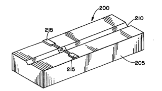
Referring now to Fig. 2a, a fusion block 200 is shown comprising a
~ substrate of a material such as alumina. A pair of conducting
electrodes 215 overlies and is preferably bonded to a flat surface of the substrate on
either side of a pass line defined by a V-groove 210. The V-groove 210 serves as a
guide for guiding and aligning two fibers to be fused into position. Fig. 2b is sirnilar
to that of 2a and includes a top layer of alumina 220 covering and - '.s. ' _ the
electrodes. r . ~ results have shown that a more controlled arc is obtained
during fusion with a top layer covering the alumina 220.
By using a substrate 205 having a flat or nearly flat upper surface, strips or
sheets of copper can be overlaid and bonded to one or more larger sheets of substrate
material to provide an array of blocks, that can be separated into individual fusion
blocks. By way of example, Flg. 3a is illustrative of a copper pattern formed from a
sheet of copper 300. Similar copper patterns can be fomled by chemical etching, or
by die stamping. This pattern sheet 300 is bonded to a non-conducting substrate
2 o layer, and is later cut into individual fusion bloclcs. A dotted line 305 in Fig. 3a
shows the outline of a pattem used for one fashion block shown in Fig. 3b. A trench
or V-groove 310 defining a passline and a guide for the optical fibers to be fused,
indicated by a dotted line in Fig. 3b, can be cut into the block to expose electrode tips
360.
2s Referring now to Fig. 4, an alternative fusion block is shown in two sections
that during assembly are bonded together. A bottom section comprises a ceramic
V-block 400 with a wide channel 410 cut through a central region for - ' _
a multi layer top section 440 to be glued therein. The multi layer top section 440 is
comprised of a bottom layer 442 of BeO or alumina that serves as a heat dissipation
3 o layer. A pair of electrodes 445 lie over the bottom layer and are initially deposited as
a single copper strip. The copper strip is severed into the pair of electrodes 445 when
the notch 460 is cut into the multi layer top section 440. A~er the top and bottom
S~J~ E ' ~ L- 'v,
2 ~ ~7 1 82
WO 96105516 PCI/CA95/00474
~ctions 400 and 440 are joined together, the notch 460 serves as an arc region across
which a fusion arc is formed when a suitable voltage is applied across the electrodes
445. A top layer of Borosilicate glass 447 is bonded to the electrodes and to the
bottom alumina layer. A transparent window may be provided for viewing the fibers
to be fused together. The top layer 447 may also be a layer of alumina adjacent to the
electrodes, for enhanced heat dissipation and a top layer of glass provided to retain
. By cutting a larger block of substrate material into an array of top
sections 400 or bottom sections 440, they can be fabricated in large quantities at the
sllme time.
lo Referring now to Pigs. 5a and 5b, an alternate preferred; bc " is
shown. For the purposes of illustration and of as~mbly, the fusion block is shown as
an upper block S00 and a lower block SS0 that are to be bonded together.
Ad. ~ '~, this ' ' provides electrode contact pads S63 (one of which
is shown) on an underside of the lower block 550 that have a large surface area for
rnaking electrical contact with a voltage source.
The lower base block SSS, is comprised of a tbick lower slab SS1 of suitable
non-. ' ~ heat dissipating material such as alumina. A planar copper layer SS2
is bonded by way of being deposited or glued to the top of tbe lower base block S50.
An upper layer of alumina 554 covers the copper layer 552 forrning a copper
2 0 sandwich between layers of alumina 551 and 554. An a~al groove 555 is cut into the
ba~ block 550 through the copper layer 552 thereby forming two dectrode tips SS6(one of which is shown). A portion ofthe electrode body S58 fans out and rnakes
contact with a copper connecting track 560, however, an dongate electrode body
could be used in place of the more triangular one shown. A copper plated barrel
lining a through hole 561 forms an electrical path between the copper cormectmg
track 560 and a copper contact layer that forrns the contact pad 563 disposed at an
end on the bottom of the base block 550. The structure is L, ~ ' and the other
electrode (not shown) makes electrical contact via a copper plated barrel lining a
through hole with a contact pad disposed at the other end of the block.
3 o The upper block 500 is comprised of a slab or block of alumina or like
material and is shown with a section cut out of a side of its mid-region. Duringfabrication of the fusion block, the upper block 500 is in~rted and bonded into the
2 1 q7 ~ 8~
~ WO 96105526 PCT/CA95/00474
axial groove of the lower block S50, the top portion S02 is ground offand a V-groove
504 is ground along the l ' axis of the upper block 500. The two portions
515 and 517 shown in dotted outline are all that remains after the top is ground off.
The gap 520 between the two portions 51S and 517 forms an arc cavity.
Referring to Fig. 5b, a top view of the fusion block of Fig. 5a is shown. The
copper on the back surfiue forrning the contact pad 563 provides a large area for
contacting with a suitable voltage supply or sound. The plated through hole 561
adjacent each end provides a conducting path from the lower contact pad 563 layer
through the substrate to the electrode layer.
By using slabs of material that have ' ' ",~ planar sorfaces, arrays of
blocks can be fabricated out of laminates of non-conducting substrate and conducting
copper track material. Such an array is shown in Fig. 5c. From the four (4) inch by
four (4) inch substrate shown, 12 x 31 fusion blocks can be fabricated by cutting the
substrate av!vulP '~, into rows and columns.
Fig 5d is a diagram of a block similar to the one shown in Fig. 5a, however,
the block of Fig. 5d is absent a covering surface. The block 570 also resernbles the
one depicted in Fig. 2a but includes plated barrels lining through holes that make
contact with large conducting contact pads on the bottom of the block (not shown).
Referring now, to Fig. 6, an alternate; ' " is illustrated, comprised of
a slab or block of alumina 600, similar to the block 200 shown in Fig. 2a. Electrodes
645 are cut out of a sheet of copper and formed over the block. The electrodes each
include a tip 656, a side portion and a contact surface 663 for contacting a voltage
source. A cerarnic top 665 is provided having a cavity slot and a viewing port 668.
The opening defined between the electrode tips 656 can be covered by a glass cover
670 that fits over the ceramic top 665. In all of the ' " heretofore described
in r ' with this invention, it is preferable, but not essential, that the copperelectrode layer be directly physically bonded to at least one layer of ceramic substrate
material to enhance heat transfer. Referring now to Fig. 7a, a copper electrode tip 756
is shown surrounded by epoxy 758 ~s.:vh-vd between an upper and a lower ceramic
3 o layer 760 snd 762. Although this u o~ is functional, a large amount of epoxy
is burned up or otherwise destroyed when the copper electrode tip reaches a highL~ v aLul v lirniting the heat transfer. In the preferred b~ " of Fig. 7b, the
; ~J~ T~JTE Sh~LI ~F:J~
2 1 ~7 ~ ~2
WO 96105526 PCTICA95100474 '
dectrode tip 756 is shown physically bonded to a lower heat dissipating layer 762 of
ceramic by way of being c~ , ' ' and fired for optimum adhesion.
Turning now to Figs. 8a and 8b, two alten~ate electrode 85G 6,, are
shown. In each of these figures, the corner of the electrode serves as the electrode tip.
S When a suitable voltage is applied, the air across the gap iol~izes and an arc
8S8 occurs across the tips. The voltage necessary to initiate and rnaintain the arc,
depends on the gap width among other physical factors.
Of course, numerous other: ' ' may be envisaged without departing
from the spirit and scope of the invention. For example, any of the ' "
shown in Figs. 4, 5, 6, and 8, could also be '' tli without a top sheet above
the electrodes. As well, the blocks, shown could also be ~ tli with one or
more aligmnent grooves to ' a plurality of optical fibers, for example to
r ' ' ribbon fiber fusion ,, ' Although in most of the . ' ~ "
shown, the electrode cross section is l~ _ ' square or circular cross sections or
others can also be used. The fusion blocks shown in typical block shaped elements,
however, within the scope of this invention the definition of a block e r all
forms or elements having one or more ' 'l~ planar sides.
By overlaying elongate electrode material over a ' _ substrate, a
convement, , 1:.,, ' ' fusion block is provided.
The invention has been described with reference to the preferred
Obviously ' " and alterations will occur to others upon the
reading and I ' ' _ of this ~ ;. - It is our intention to include all such
' ~ and alterations insofar as they fall within the scope of the appended
clauns or the equivalents thereof.