Note: Descriptions are shown in the official language in which they were submitted.
WO 96/16456 2 2 0 1 6 2 2 . ~ rCT/CA95/00569
OPTICAL Q~ ~ TO ~R~R~'I'R
ULTRA SEORT PULSES IN DIODE LASERS
5 Field of the Invention
This invention relates to S~m;,-nn~llctor lasers and
more particularly to a system wherein a s~m;~nn~ tor laser
is Q-switched optically by a second semiconductor laser to
generate an ultra short pulse.
Back~rolln~ of the Tnvention
In the tel.-c, ln;cations industry, there is an
on-going requirement to increase the tr~n~m; cc; on bandwidth
so as to allow the delivery of greater communication
15 services such as video, and high density computer data.
Single moae optical fibers are known to be an iaéal meaium
for the transmission of wide bandwidth data and,
consequently, transmission systems speci-fically desIgned to ~_
take advantage of this property are-continually being
20 developea. Such systems include wavelength division
multiplexing (WDM) and time division multIpIexing (TDM~
photonic networks . In return to zero =I:RZ ) coding and pulse
position coding (PPC) the shorter the pulse width of the
data train the shorter the time slot and hence the greater
25 the overall capacity of the TDM systems. ~ ~
Further, in optical information processing and
optical computing systems shortening the bit length in the
time axis can speed up the processing or computing. It may
30 also provide processing accuracy through precise signal
triggering by the short pulses. ~-
The present invention rela~es to a-system wherein
ultra short pulses are generated optïcally by utilizing the
35 output of one semiconductor laser to effect Q-switching of
another semiconductor laser. In aadition, the system is
capable of wavelength conversion between the wavelengths of
the two lasers.
Wo 96/16456 PCT/CA95/00569 ~
2201 622: 2 - ~ -
Prior Art
It is known to Q=switch solid state lasers with
the output of semiconductor laser diodes in~ order = to
increase peak power output and/Qr decrease pulse wïdth.
In reissue US Patent 34, i92 dated March 9, 1993
(T.M. saer) a laser dioQe is used tQ. end pump a rod of
Nd:YAG or Nd:YLF to produce an output pulse~having~a pulse
width in the order o 50 ns.
In US Patent 5,265,115 which issued November 23,
1993 tQ Amano, a- semiconductor laser is~used to pump a solid
state laser medium in a laser resonator. The combination is
used to ~eep the intensity Qf an out~put laser beam
substantially invariable regardless of the oscillation
condition.~
US Patent 5,283,8~1 which issued February 1, 1994
to Mecherle, discloses a system wherein a laser diode is
used in ~n external resonant ring cavity in order to produce
cavity dumpïng or Q-switching.
US Patent 5,317,447 which issued May 31, 1994 to
Baird et al discloses a diode-pumped tunable~solid sta.e
laser which in one embodiment provides a frequency
conversion from an infrared output of the laser diodes to a
visible or near ultraviolet output.
None of the pr~or~a-rt of which Appli~ants are
aware utilizes a speciaLly designed multi-segment dlode
laser which is optically Q-switched by a diode probe laser
in order to generate ultra short output pulses.
Summarv of the Invention
~ - It is an object of the present invention to
provide a system in: which a diode laser is optically~ Q-
switched by another diode iaser.
~ Wo 96/16456 2 2 0 1 6 2 2 ~ PCT/CA95/00569
It is a further obj ect of the invention to provide
a width compressed short optic21 pulse in the order of 65 ps
(FWE~M) by pumping light from a prQbe laser into: a specially
designed signal Iaser.
It is a still further Qbject of the invention to
provide a wavelength conversion by pumping a signal laser
having an output of a first wavelength with light of a
second wavelength from a probe laser. In p~actice the
10 conversion is in the range 5-50 r,m whiIe in principle it is
only limited by the gain spectrum.
Therefore in accordance~with a first aspect of the
present invention there i~ provided a system ~for optically
15 generating a shQrt width optical pulse. The system has a
first distributed feedback (DFB) semiconductQr iaser (signal
laser) having a multi-quantum-well (MQW) active region to
produce a ' laser output of a first wavelength in response to
an injected current, the first laser having a common contact
20 of one polarity and a pair of isol~ated contacts ~of the
opposite polarity. Means are provlded to separately supply
injection current to each one of the p:alr of lsolated
contacts . The system alsQ= has a second DFs laser (probe
laser) which has an active region to::produce a Iaser output
25 of a second wavelength in response to an injection current
supplied to a contact therecn: In~ a pref erred embodimënt
the second wavelength is longer than the first. A
modulating input current is providèd-~to the second laser by
appropriate supply means. Optical transfer means which in a
30 preferred embodiment cQmprises a single mode fiber,
isolator, tunable: attenuator, pQlarization controller and
fiber coupler, is used to couple light from the active
reg~on of the second laser to the: active region of the first
laser.
In accordance with a second aspect of the
invention there is provided a method of generating a short
WO 96/16456 PCT/CA9S/00569 ~
220 ~ 62~ - -
width optical pulse ~e.g.,=65 ps) by Q-switching a signal
laser with the light from a probe laser. Accordil~-g to the
method a DFB semiconductor-signal laser havlng a MQW active
area is operated by supplying separatel~y controlIable bias
5 current to a pair of i q~ =P-l contacts= of ol:le polarity on
the device in order to generate an output of a first
wavelength. A second DFB diode laser is operated with a
modulating current in order to produce an oùtput of a second
wavelength. Preferably the second wavelength is longer than
10 the first. The output of the second laser is optically
coupled to a cavity of the f irst in order to proviae a Q-
switching function. =
Desc~i~tion of the Drawinqs ' ~ ~
15 ~ : The invention wlll now be described in greater=
detail with reference to th~ appended drawings wherein:
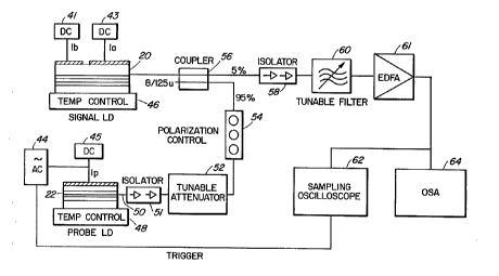
FIGIJRE 1 is a:block diagram of the laser-system
according to the invention;-
FIGURE 2 is a perspectlve view of the signal
20 laser; ~
FIGURE 3 illustrates the wavelength~haracteristics of the signal laser operating with and
without optical input from the probe laser; ~~ --
FIG~iRE 4 is the output waveform of the prsbe
25 laser;
FIGURE 5 is the output waveform of the signal ~
laser as pumpea with the waveform of FIGURE 4; and
FIGURE: 6 shows graphically the output power
dependence of the signal laser upon the - input power .
Detailed Descri~tion of the~Invention
FIG~RE l illustrates in b~ock form the various
elements in the preferred embodiment of the invention.
These~eIements incIude signaq laser 20 and probe laser 22.
35 For a~ better understanding of the signal laser, reference
may be made to FIGURE 2. The signal laser 20 in a preferred:
embodiment is based on the~ InGaAsP/InP system and the MOCVD
~ Wo96116~56 PCr/CA95/00569
-- 22(~1622 - 5 - ~
growth procedure_: It is to be understood, however, that
other semiconductor materials and growth techniQues may be
used in the preparation of both signal and probe lasers.
For example, the Quantum well structure may incorporate
5 = InGaAs in which case the III-V alloy system may be defined
as InGaAs / InGaAs P / InP .
As illustrated in FIGURE 2=, signal laser 20 has
multi-Quantum-well active region 24 consisting of four 5.5
nm thick l . 5% compressively strained InGaAsP QUantum wells
26 and three unstrained InGaAsP (~g = 1.25 llm) barriers 28 .
Again, this is exemplary only and the invention is not
limited to such a structure. A first order grating 30 for
the index coupling with a depth of approximately 65 nm was
formed in p-type InGaAsP iayer 32. The grating was formed
by photolithography and wet chemical etching. A p-type InP
layer is grown on top of the grating followed by a p-type
nGaAs contact layer. =A ridge waveguide2structure 34 is
formed in the structure for lateral optical confin~ - t.
~ ~~
sio2 and Au/Cr are employed to~-form p-type
contacts as is well known in the prior~art. An n-type
contact is fQrmed on the InP substrate ~side.
: The ridge waveguide 34 was partitioned by ion
reactivP e~ in~J channel 36 thereby creating a pair of
segments~ 38 and 39 having isolated conta=cts 40, 42
respectively. In the exemplary embodiment discussed herein
segments 38 and 39-are 240 ~Lm and:l20 llm long respectively.
Ridge waYeguide 34 has a ~nominal width o:f 2 ~lm. The facet
43 of segment 38 was coated with 5~6 anti reflec~tivity and
used as the front facet . q he isolation ~esistance between
se~ments 38 and 39 was approximately 800 Q~ The resistance
stated is by way of example only and the invention is not
limIted to this value, a resistance greater than 200 Q is
considered adequate. The wavelength of iaser 20 was
approximately 1563 nm as shown in FIGI~RE 3. In this figure,
Wo 96116456 PCT/CA95100569
2201622 ~ 6 ~ ~~
wave~orm A illustrates the wavelength peaks with optical
injection from probe laser~22 while waveform s shows the
relative peaks without any optical input from the probe
laser .
Probe laser 22 preferably has a distributed
feedback (DFB) structure ~ith grating 30 but without
segmented waveguide. The ~avelength of laser 22 was
approximately 1580 nm.
As shown in FIGURE 1 the signal laser 2(~ is
provided with separately controlled d. c . current via
supplies 41, 43 to both con~acts 4D, 42 . Probe laser 22 is
supplied with a d.c. bias curre`nt from supply 45 and a
15 modulating component provlded by an a.c. controller 44.
Both laser 20 and 22 are temperature :controiled with Peltier
devices 46 and 48 respectively.
The output of probe laser- 22 is cQupled:to signal
20 laser--2~ through single mode =optical fiber 5~= via an
isolator 51, a tunable attenuator 52, polarization control
54, and fiber coupler 56.- The coupler 56 has SgO and 9s%;
output ends as indicated in FIGURE 1. The output Qf signal
laser 20 through coupler 55 is transferred tQ optical
2s isolator 58, and through tunable wavelength filter 60 and
magnified by an erbium doped fiber amplifier (EDFA) 61. The
waveform o the signal is measured with a sampling
osc~lloscope 62 equipped ~ith a 22 GHz canverter~sampling
head. ~ wavelengths of optical signa:,s are monitored with an
30 optical spectrum analyzer 64. ~
In the set-up discussed herein, probe laser 22 is
modulated at a 500 Mbit/s rate: wlth a 50% duty cycle giving
an optical output signal shown~ by the waveform of FIGURE 4 .
35 The signal laser 20 is operated under CW conditions with
different injection current levels supplied to the isolated
p-type contacts.
Wo 96/16456 PCT/CA95/00569
220 1 62=2
The drive conditions for the slgnal laser in order
to accomplish the results reported hereIn were 42 mA for
segment 38 and~ 28 mA for segment 39 . ~he operating
- temperature was 25 . i50C . As discussed previousiy these
5 values are exemplary only and not intended to be limiting.
Under these conditions the output of the signal laser
switches from the 50% duty cycIe of the probe lasér to the
narrow pulse shown in the waveform of F:~GURE 5. The output
pulse wldth is measured at 65 ps (FW~) while the ~a~ling
10 time o~ the input pulse was about 200 ps . The system ~ s
mi nAnt wavelength switched from the 1563 nm signal laser
output to 1580 nm, which is the wavelength of the probe
laser .
The foregoing results are explained as follows.
When the signal laser is pumped at certain fevels above
threshold both the optical gain and the phase for a signal
wave making a round trip in the ~avity can be controlled by
an external optical signal. If the signal laser is designed
20 to have a large wavelength detuning from the~gain peak, one
has to pump more carXiers to satisfy the=lasing condition.
This, on the other hand, can amplify the probe laser light
injected ~ro=m outside. Because the probe light shares the
carriers (optical gàin~ with the original si~gnal light, the
25 presence of the probe light can quickly decrease the Q value
of the overail laser cavity and lead to ~n optical Q-
switching. It is believed that the narrow pulse: width is
due both to the ~QW laser structure and the multiple Bragg
modes in the two-segment DFB signal laser 20. In a MQW
30 structure carrier life time is normally smaLler and the
carriers are pre~lr,minAn~ly locaIized in the wélls as
compared to `its :bulk counterpart. ~hus, eve~ though the
laser bias level approached thresho1d during the Q-switching
process it was still poss1ble to observe a short width pulse
35 with high sensitivity. The multiple sragg modes contribute
to the ef f ect in as much as, when the probe laser signal
turns off, the existence of other longitudinal modes enhance
Wo 96/164S6 PCT/CA9S/00569 --
220 1 ~22 -- ~
f g
the operation speed by gain rnh~nr --t because the device
is always operating- in an ~ on ~ state . These modes ~can
become either stronger or weaker depending ol~ the new phase
conditions in the cavity.
5 ~
The system of the present invention has several
advantages over the prior art techniques for generating
short pulses. Firstl~ the system is completely optical,
thus avoiding limitations inherent in traditional electronic
10 switGhing networks. secondly the wavelength is convertible,
i.e., ~the output waveIength is aifferent than the input
wavelength. Further, because of optical triggering the.
restrictions in modulation speed imposed by parasitics is
relaxed. Since no electrica:L to optical conversion
15 components are required the: system is more cost ef f=icient .
Finally, the system provides a s`lmple technique of
generating pulse compression.
Although a particular embodiment of the invention
20 has been illustrated and described it will be apparent to
one skilled in the art ~that-changes to the system can be
made. It is ahticipated~ however, =that such changes will
fall within the scope of the invention as defined by the
fQllowing claim~s. -