Note: Descriptions are shown in the official language in which they were submitted.
CA 02206693 2003-10-16
SPECIFICATION
Point of Origin Conualler
FIELD OF ARTS
This invention relates to a game machine system having an operating device.
More particularly, this invention is concerned with a game machine system
including a
game machine, such as a personal computer or a video game apparatus, and an
operating
device (controller) for traasmittin~g and receiving every data to and from the
game
machine.
la
PRIOR ARTS
fiigure 1 is a connection diagram of a conventional game machine (for example,
an
electronic. game apparatus) and a controller. In the figure a CPU 81 (Central
Processor
' Unit) writes data into a W~RAM 83, reads data out of the W-RAM 83 and
transmie data co
a PPU-84 (Picnue Processing Unit), is synchronism with a clock acid according
to
program data stored in a ROM 82 (Read Only Memory), to thereby generate a
picture
image signal to the PPU 84 based on an image data in a V-RAM 8S. The CPU 81
also
transmits a cloak signal to a controller 90A or 90B to directly receive data
such as on
switches pperated by an operator in synchronism with the clock The CPU 81.
outputs
data to PPU 84 so as to cause change in au image signal in accordance with the
data
inputted from the controller 90A or 908.
As clear fram the above configuration, the game machine and the eontmllers 90A
and 90B are connected therebetween by a data line for receiving operating
device data
from the controllers 90A and 90B and a caock signal line for transmitting to
the
2S controllers 90A and 908 a clock signal for syncluonizing timing of
transmission of data
I
,s CA 02206693 1997-06-03
from the controller and timing of operation of the CPU 81. The data line is
connected
directly to the CPU 81 via an interface (not shown). In other words, in the
conventional
game machine system, the data of the controllers 90A and 90B are read directly
by the
CPU 81 itself performing image processing at timing based on the clock.
Consequently,
the CPU 81 has to directly read the signal from the controllers 90A and 90B,
thus
increasing the amount of processing by the CPU 81. Furthermore, the CPU 81 has
to read
the signal from the controller in synchronism with the clock, so that there is
a necessity of
a clock line, in addition to the data line for transmission and reception of
data. To this
end, there is increase in the number of pins of a connector for connecting
between a cable
and the game machine, raising manufacturing cost. Furthermore, the
conventional
controllers 90A and 90B are each provided with a plurality of switches and
transmission
is only on data, as to whether an individual switch is depressed or not, to
the main-body
game machine.
Conventionally, there has required time for which the CPU reads controller
data,
as the data amount for the controller increases. Thus, the CPU has imposed by
increased
processing amount.
Moreover, conventionally, the clock signal line is required in addition to the
data
line for connection between the controller and the game machine. To this end,
the
number of pins of the connector connecting between the controller and the game
machine
is increased, and manufacturing cost is expensive.
In addition, among the conventional controllers there has not existed such
controller that is excellent in such extendibility that makes possible
transmission and
reception of various data without limitation to transmission of data on
whether or not an
individual switch is depressed. Under such circumstances, it has been
impossible to
realize a variety of methods of use by extending in various ways after
purchasing the
2
r ,~ CA 02206693 1997-06-03
r
controller.
SUMMARY OF TI-IE INVENTION
It is therefore an object of a first invention to provide a game machine which
is
capable of reducing the amount of processing in the CPU to secure sufficient
time for
spending inherent image processing in the CPU.
It is an object of a second invention to provide a game machine system which
is
capable of reducing the amount of processing in the CPU to secure sufficient
time for
spending inherent image processing in the CPU, and reducing manufacture cost
by
reducing the number of pins in a connector for connecting between a controller
and the
game machine. Also, to provide a game machine system in which a variety of
using
methods can be realized by extending the controller in various ways.
A first invention, in a game machine which is connected to a plurality of
operating
devices adapted to be operated by an operator and output, by modulation,
output device
data representative of an operating state of the operating device (40) 'by
receiving
command data, to perform image processing based on the operating device data,
comprises: a central processing means (11), an operation storing means (14), a
receiving
means (173), a temporary storing means (174), a data processing means (171),
and
transmitting means (172).
The central processing means is arranged to operate for image processing based
on
a predetermined program. T he operation storing means is arranged accessed by
the
central processing means and storable with data required for advancing a game
by the
central processing means and data from the operating device. The receiving
means
receives, by demodulation, i:he operating device data from the operating
device. The
temporary storing means temporarily stores the operating device data. The data
3
CA 02206693 1997-06-03
processing means carries out predetermined data processing according to a
command by
the central processing means. The transmitting means transmits, by modulation,
data
outputted from the data processing means to the operating device. The central
processing
means outputs command data for reading out the operating device data. The data
processing means outputs the command data outputted from the central
processing means
to the transmitting means, so that the operating device data received by the
receiving
means is stored in the temporary storing means to be transferred to the
operation storing
means at predetermined timing.
The central processing means is adapted to operate for image processing based
on
a predetermined program. The operation storing means is arranged to be
accessed by the
central processing means and storable with data required for advancing a game
by the
central processing means and data from the operating device. The receiving
means
receives, by modulation, the operating device data from the operating device.
The
temporary storing means temporarily stores command data and the operating
device data.
The data processing means carries out predetermined data processing according
to a
command by the central processing means. The transmitting means transmits, by
demodulation, data outputted from the data processing means to the operating
device.
Furthermore, the' central processing means outputs command data for reading
out the
operating device data, and the first data processing means outputs the command
data
outputted from the central processing means to the transmitting means so that
the
operating device data received by the receiving means is stored in the
temporary storing
means to be transferred to the operation storing means at predetermined
timing.
A second invention, in a game machine system structured by a plurality of
operating devices to be operated by an operator and a game machine (10) for
carrying out
image processing based on operating device data from the operating device
(40),
4
CA 02206693 1997-06-03
' comprised by the game machine, includes: a central processing means (11), an
operation
storing means (14), a first receiving means (173), a temporary storing means
(174), a first
data processing means (171), a first transmitting means (172), and a
connecting means
(181- 184); and the operating device includes: a second receiving means
(44.1), a switch
means (45, 403 - 407), a second data processing means (442), and transmitting
means
(445).
The central processing means is adapted to operate for image processing based
on
a predetermined program. The operation storing means is arranged to be
accessed by the
central processing means and storable with data required for advancing a game
by the
central processing means and data from the operating device. The first
receiving means
receives, by modulation, the operating device data from the operating device.
The
temporary storing means temporarily stores command data and the operating
device data.
The first data processing means carries out predetermined data processing
according to a
command by the central processing means. The first transmitting means
transmits, by
demodulation, data outputted from the first data processing means to the
operating
device. The connecting means connects between the game machine and the
operating
device. The second receiving means receives, by demodulation, the data from
the first
transmitting means. The switch means is to be operated by an operator. The
second data
processing means outputs operating device data as to an operating state of the
switch
means. The transmitting means transmits, by demodulation, the operating device
data
outputted from the second data processing means to the game machine.
Furthermore, the
operating device and the first data processing means are brought into
electrical
connection by connecting the operating device to the connecting means. The
central
processing means outputs command data for reading out the operating device
data. The
first data processing means outputs the command data outputted from the
central
5
CA 02206693 1997-06-03
processing means to the first transmitting means so that the operating device
data
received by the first receiving means is stored in the temporary storing means
to be
transferred to the operation storing means at predetermined timing.
According to the game machine of the present invention, the central processing
means does not perform reading-in of operating device data each time it uses
operating
device data, but the operating device data is processed by a means other than
the central
processing means. It is accordingly possible to realize a game machine in
which the
amount of processing by the central processing means is reduced to secure
sufficient time
for spending inherent game processing in the central processing means.
Also, operating device data is stored in a memory means that is stored with
data
required for advancing a game so that the central processing means is allowed
to process
operating device data similarly to other game data. Therefore-the central
processing
means can perform game processing at high speed and with high freedom.
Furthermore, according to one aspect of the present invention, operating
device
data can be partially read and accordingly there is no necessity of reading
operating
device data at its entirety at one time. Therefore unwanted portions of
operating device
data can be left unread, shortening speed of reading-in.
According to the game machine system of the present invention, since the
operating device data is processed by a means other than the central
processing means, it
is accordingly possible to realize a game machine in which the amount of
processing by
the central processing means is reduced to secure sufficient time for spending
inherent
game processing in the central processing means. Also, the operating device
data is
stored in a memory means that is stored with data required for advancing a
game so that
the central processing means is allowed to process operating device data
similarly to other
game data. Therefore the central processing means can perform game processing
at high
6
,' CA 02206693 1997-06-03
J
speed aild with high freedom. Furthermore, the number of pins in a connector
for
connecting between the operating device and the game machine is reduced to
lower
manufacture cost.
According to one aspect of the game machine system, it is possible to realize
a
variety of using methods by extending the extension device in various ways.
According to another aspect, it is possible to store data to be processed by
the
central processing means into a extension nnemory connected to the operating
device.
This therefore is effective when storing data that is different by an
operator.
According to another aspect, it is possible to memorize the data stored in an
extension memory connected to one of a plurality of operating devices into an
extension
memory connected to another operating device. This enables copying of data
between
operators.
Furthermore, according to another aspect, the data in an external memory means
is
temporarily stored in the operation storing means so that data conversion and
copy is
possible by the central processing means. This enables data to be copied in
different
format to respective external memory means.
The above described objects and other objects, features, aspects and
advantages of
the present invention will become more apparent from the following detailed
description
of the present invention when taken in conjunction with the accompanying
drawings.
BRIEF 1DESCRIPTION OF THE DRAWINGS
Figure 1 is a block diagram showing briefly an conventional art;
Figure 2 is a schematic illustrative view showing one embodiment of the
present
invention;
Figure 3 is a block diagram showing in detail an game machine in Figure 2
7
r ,' CA 02206693 1997-06-03
embodiment;
Figure 4 is an illustrative view showing a memory map in CPU of Figure 3
embodiment, demonstrating an external memory and a W-RAM incorporated in a
cartridge;
Figure 5 is a block diagram showing in detail a controller control circuit in
Figure
3 embodiment;
Figure 6 is an illustrative view showing a modulating/demodulating method for
data;
Figure 7 is an illustrative view showing a memory map of a RAM in Figure 5;
Figure 8 is 'a perspective view of a controller of Figure 3 embodiment as
viewed
from the above;
Figure 9 is a perspective view of the controller of Figure 3 embodiment as
viewed
from the bottom;
Figure 10 is a perspective view of showing an analog joystick unit capable of
being utilized in the embodiment;
Figure 11 is a perspective view showing major portions of Figure 10 unit;
Figure 12 is an exploded perspective view showing major portions of Figure 10
unit
Figure 13 is a sectional illustrative view showing major portions of Figure 10
unit;
Figure 14 is a block diagram showing in detail one example of the controller
and
an expansion device;
Figure 15 is an illustrative view showing data of the analog joystick and
respective
buttons of the controller;
Figure 16 is a block diagram showing in detail another example of the
controller
and an expansion device;
8
CA 02206693 1997-06-03
Figure 17 is a flowchart showing operation of the CPU of Figure 3 embodiment;
Figure 18 is a flowchart showing operation of the bus control circuit of the
Figure
3 embodiment;
Figure 19 is a flowchart showing operation of the controller control circuit
of
Figure 3 embodiment;
Figure 20 is a flowchart showing operation of the controller circuit of Figure
3
embodiment;
Figure 21 is an illustrative view of transmission and reception data by the
control
circuit when a command "0" is transmitted from the controller control circuit;
Figure 22 is an illustrative view of transmission and reception data by the
control
circuit when a command "1" is transmitted from the controller control circuit;
Figure 23 is an illustrative view of transmission and reception data by the
control
circuit when a command "2" is transmitted from the controller control circuit;
Figure 24 is an illustrative view of transmission and reception data by the
control
circuit when a command "3" is transmitted from the controller control circuit;
Figure 25 is an illustrative view of transmission and reception data by the
control
circuit when a command "255" is transmitted from the controller control
circuit;
Figure 26 is a flowchart showing operation of data copy;
Figure 27 is a flowchart showing a first method of origin point resetting;
Figure 28 is a flowchart showing a second method of origin point resetting;
Figure 29 is an illustrative view showing the correspondence of a physical
coordinate of the joystick to a display screen;
Figure 30 is an illustrative view showing the correspondence of the physical
coordinate of the joystick to the display screen when resetting an origin
point;
9
CA 02206693 1997-06-03
EMBOIDIMENTS
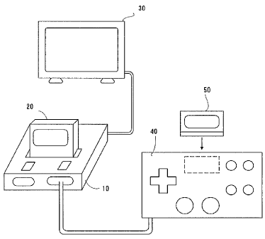
Figure 2 is is an external appearance showing a system arrangement of a game
machine system according to one embodiment of the present invention. The game
machine system is for example a video game system, which inclusively comprises
a game
machine 10, a ROM cartridge 20 as one example of an external memory device, a
monitor
30 as one example of a display means connected to the game machinel0, a
controller 40
as one example of an operating device, and a RAM cartridge 50 as one example
of an
extension device detachably attached to the controller 40. Incidentally, the
external
memory device stores image data and program data for image processing for
games, and
audio data for music, effect sound, etc. A CD-ROM or a magnetic disc may
alternatively
be employed in place of the ROM cartridge. Where the game machine system of
this
example is applied to a personal computer, an input device such as a keyboard
or a mouse
is used as the operating means.
Figure 3 is a block diagram of the game machine system of this example. The
game rrlachine 10 incorporates therein a central processor unit (hereinafter
"CPU") 11
and a bus control circuit 12. The bus control circuit 12 is connected with a
cartridge
connector 13 for detachably attaching the ROM cartridge 20, as well as a
working RAM
14. The bus control circuit 12 is connected with an audio signal generating
circuit 15 for
outputting an audio signal processed by the CPU 11 and a video signal
generating circuit
16 for outputting a video signal, and further with a controller control
circuit 17 for serially
transferring operating data of one or a plurality of controllers) 40 and/or
data of RAM
cartridges) 50. The controller control circuit 17 is connected with controller
connectors
(hereinafter abbreviated as "connectors") 181 - 184 which are to be provided
at a front
face of the game machine 10. To the connector 18 is detachably connected a
connection
jack 41 and the controller 40 through a cable 42. Thus, the connection of the
controller to
,' CA 02206693 1997-06-03
a
the connector 181 - 184 places the controller 40 into electric connection to
the game
machine 10, enabling transmission and reception of data therebetween.
More specifically, the bus control circuit 12 inputs therein a command
outputted
by a parallel signal from the CPU llvia a bus to parallel-serial convert it
for outputting a
command by a serial signal to the controller control circuit 17, and converts
serial signal
data inputted from the controller control circuit 17 into a parallel signal
for outputting it to
a bus. The data outputted through the bus is subjected to processing by the
CPU 11,
stored in W-RA1VI 14, and so on. In other words, the W-RAM 14 is a memory
temporary
storing the data to be processed by the CPU 11, wherein read-out and write-in
of data is
possible through the bus control circuit 12.
Figure 4 is a diagrammatic illustration showing memory regions assigned to
respective memory spaces. The memory spaces accessible by the CPU via the bus
control circuit 12 involves an external memory region of the ROM cartridge 20
and a
memory region of the W-RAM 14. Although the ROM cartridge 20 is structured by
mounting on a board a ROM stored with data for game processing and
accommodating
the same board in a housing, the ROM storage data is shown by the external
memory
region shown in Figure 4. That is, the ROM includes an image data region 201
stored
with image data required to cause the game machine 10 to generate image
signals for the
game, and a program data region 202 stored with program data required for
predetermined operation of the CPU 11. In the program data region 202, there
fixedly
stored are an image display program for performing image display based on
image data
201, a time-measuring program for carrying out measurement of time, and a
determination program for determining that the cartridge 20 and an extension
device 50,
hereinafter referred to, are in a predetermined relationship. Incidentally,
the details of the
time-measuring program and the determination programs will be stated later. On
the
11
~' CA 02206693 1997-06-03
A
other hand, the memory region of W-RAM 14 includes a region 141 for
temporarily
storing data representative of an operating state from a control panel.
Figure 5 is a detailed circuit diagram of a controller control circuit 17. The
controller control .circuit 1'7 is provided for transmission and reception of
data in serial
between the bus control circuit 12 and the controller connector 181 - 184, and
includes a
data transfer control circuit 171, a signal transmitting circuit 172, a signal
receiving
circuit 173 and a RAM 174 for temporarily storing transmission and reception
data. The
data transfer control circuit 171 includes a parallel-serial conversion
circuit and a serial-
parallel conversion circuit for conversion of data format during data
transfer, which also
performs control of write-in and read-out of the RAM 174. The serial-parallel
conversion
circuit converts serial data supplied from the bus control circuit 12 into
parallel data to
provide it to the RAM 174 or the signal transmitting circuit 172. The parallel-
serial
conversion circuit converts parallel data supplied from the RAM 174 or the
signal
receiving circuit 173 into serial data to provide it to the bus control
circuit 12. The signal
transmission circuit 172 converts data for signal read-in control of the
controller 40
supplied from the data transfer control circuit 171 and write-in data
(parallel data) to the
RAM cartridge 50 into serial data, which data is transmitted through a
corresponding
channel CH1- CH4 to each. of the plurality of controllers 40. The signal
receiving circuit
173 receives in serial read-out data, representative of an operating state of
each of the
controller 40, inputted through a corresponding channel CH1 - CH4 to each of
the
controller 40 as well as read-out data from the RAM cartridge 50, to convert
them into
parallel data to provide it to the data transfer control circuit 171.
The signal transmitting circuit 172 and the signal receiving circuit 173 adopt
a
duty-cycle modulation and demodulation (hereinafter referred to as
"modulation/demodulation") method as one example of the
modulation/demodulation
12
'~ CA 02206693 1997-06-03
- method. The duty-cycle modulation/demodulation method, as shown in Figure G,
is a
modulation/demodulation method wherein "1" and "0" are represented by varying
a Hi
time period and a Lo time period for a signal at a certain interval.
Explaining the
modulation/demodulation method with more detail, when data to be transmitted
in serial
is a logical "1" a signal having, within one cycle period T, a high-level
period tH rendered
longer than a low-level period tL (tH > tL) is transmitted, while when data to
be
transmitted is a logical "0" a signal having, within one cycle period T, tH
rendered shorter
than tL (tH < tL) is transmitted.
In the meanwhile, the demodulation method makes sampling on a serial signal
received (bit transmission signal) so as to monitor at all times whether the
received signal
is at a high level or a low level, wherein one cycle is expressed as T = tL +
tH provided
that time period of low till change to high is tL and time period of high till
change to Iow
is tH. In this case, the relation of tL and tH being tL < tH is recognized as
logical "1",
while tL > tH is recognized as logical "0", thereby achieving demodulation. If
the duty-
cycle modulation/demodulation method like this is employed, there is no
necessity of
transmitting data in synchronism with clock, offering an advantage that
transmission and
reception of data are available with only one signal line. Incidentally, it is
natural that if
two signal lines are available another modulation/demodulation method may be
utilized.
The RAM 174 includes memory regions or memory areas 174a - 174h as shown in
a memory map of Figure 7. Specifically, the area 174a is stored with a command
for
channel 1, while the area 1'74b is stored with transmission data and reception
data for
channel 1. The area 174c is stored with a command for channel 2, while the
area 174d is
stored with transmission data and reception data for channel 2. The area 174e
is stored
with a command for channel 3, while the area 174f is stored with transmission
data and
reception data for channel 3. The area 1748 is stored with a command for
channel 4,
13
,' CA 02206693 1997-06-03
Gf b
while the area 174h is stored with transmission data and reception data for
channel 4.
Accordingly, the data transfer control circuit 171 operates to write-in
control to the
RAM 174 data transferred from the bus control circuit 12 or data of operating
state of the
controller 40 received by the signal receiving circuit 173 or read-out data
from the RAM
cartridge 50, and read data out of the RAM 174 based on a command from the bus
control
circuit 12 to transfer it to the bus control circuit 12.
With referring to Figure 8 and Figure 9, the controller 40 of this embodiment
shown includes a housing 401 consist of an upper half and a lower half. At
both left and
right ends of the housing 401, a left grip 402L and a right grip 4028 are
respectively
formed in a manner that the same are protruded toward a front side. An
intermediate
position between the left grip 402L and the right grip 4028, a center grip
402C is formed
in a manner that the same is protruded toward the front side. A cross-
direction
designation switch 403 which is a digital joystick is formed on a surface of
the housing
401 in the vicinity,of a base end of the left grip 402L. Action designation
switches 404A,
404B, 404C, 404D, 404E and 404F which designate six (6) kinds of actions are
respectively formed on the surface of the housing 401 in the vicinity of a
base end of the
right grip 4028.
An analog joystick 45 which is capable of designating all directions within
360
degrees is formed on the housing 401 in the vicinity of a base end of the
center grip 402C.
At an approximately central position of the housing 401, a start switch 405
which
designates a start of a game is formed. Furthermore, the start switch 405 is
positioned at
an approximately center of an area surrounded by the switches 403 and 404A to
404F,
and the analog joystick 45.
Furthermore, a pair of side surface switches 406L and 4068 are formed on a
rear
surface of the housing 401, and a bottom surface switch 407 is formed at an
14
CA 02206693 1997-06-03
K a
approximately center of the lower half in the vicinity of the base end of the
center grip
402C.
A rear surface of the lower half is extended toward direction of a bottom
surface,
and an opening portion 408 is formed at a tip end thereof. In an interior of
the opening
portion 408, a connector (not shown) to which an expansion cartridge 50 shown
in Figure
4 is connected is provided. Furthermore, a lever 409 for discharging the
cartridge 50
inserted into the opening portion 408 is formed at a position of the opening
portion 408.
In addition, at a side opposite to the lever of the opening portion 408 to
which the above
described expansion cartridge 50 is inserted, a notch 410 is formed, and the
notch 410
secures a space for withdrawing the expansion cartridge 50 in discharging the
expansion
cartridge 50 with utilizing the lever 409.
Now, with referring to Figure 10 to Figure 13, the analog joystick 45 will be
described in detail. The analog joystick 45 is constructed as a joystick unit
shown in
Figure 19. The joystick unit is sandwiched by the upper half and the lower
half of the
housing 401. The joystick unit includes a housing formed by a case 451 and a
cover 452,
and an inner case 453 are accommodated within the housing.
As shown in Figure 11 and Figure 12, the inner case 453 includes a bowl-shaped
recess portion 454 formed at a center of the inner case 453, and there are
provided with
tvo pairs of support plates 455a and 455b, and 456a and 456b around the recess
portion
454 with angle-interval of 90 degrees, and semicircular bearings 457a and
457b, and 458a
and 458b are formed on the support plates 455a and 455b, and 456a and 456b,
respectively. The bearings 457a and 457b or 458a and 458b are arranged on the
same
axis line, and axes of the bearings 457a and 457b, and 458a and 458b are at
the same
height level, and orthogonally intersected to each other. Wheels 459 and 62
having
rotation shafts which are orthogonally intersected to each other are rotatably
supported at
xY CA 02206693 1997-06-03
4,
~ a side surface of the inner case 453, and gears 461 are uniformly formed on
the respective
wheels 459 and 460.
The analog joystick unit further includes swingable members 462 and 463. One
swingable member 462 is formed by an arc-like member which is provided with a
long
hole 464 being made long in a longitudinal direction of the arc-like member,
and
supporting shafts 465a and 465b are formed at both ends of the swingable
member 462,
and shaft end portions 467a and 467b respectively having flat surfaces 466a
and 466b are
extended from the supporting shafts 465a and 465b, and a sector gear 468 is
provided on
one shaft end portion 467b. The other swingable member 463 is different from
the one
swingable member 462 in a point that the swingable member 463 is constructed
by an
arc-like member having a radius of curvature smaller than that of the
swingable member
462; however, in other points, the swingable member 463 is constructed in a
manner
similar to or the same the swingable member 462. That is, a reference numeral
469
denotes a long hole, reference numerals 470a and 470b denote supporting
shafts,
reference numerals 471a and 471b denote flat surfaces, reference numerals 472a
and 472b
denote shaft end portions, and a reference numeral 473 denotes a sector gear.
The supporting shafts 465a and 465b, and 470a and 470b are individually
inserted
into the two sets of bearings 457a and 457b, and 458a and 458b of the inner
case 453, and
therefore, the part of the swingable members 462 and 463 can be supported in a
swing-
free fashion, and the swingable members 462 and 463 are arranged in a state
where
longitudinal directions of the long holes 464 and 469 are orthogonally
intersected to each
other and overlaid with an interval or gap. In the pair of swingable members
462 and 463
thus attached to the inner case 453, the sector gears 468 and 469 bite the
above described
gears 461. Furthermore, respective ones of the above described flat surfaces
466a and
466b, and 471a and 471b are included in the same horizontal plain in a neutral
state of a
16
.' CA 02206693 1997-06-03
lever 474 (described later).
As shown in Figure 12, the lever 474 includes protrusions 475 which are
protruded
toward outer radius directions at one end of the lever 474, and a ball portion
476 at a
middle portion of the lever 474, and a connection portion 477 at the other end
of the lever
474. Grooves 478 which a.re extended in a latitude direction at positions
apart from each
other by 180 degrees are formed on the above described ball portion. 476. A
diameter of
the lever 474 is selected at a size which is not larger than sizes of short
directions of the
long holes 464 and 469 formed on the swingable members 462 and 463.
Preferably, the
diameter of the lever 474 is selected at a size by which the lever 474 can be
slidably
inserted into the long holes 464 and 469 with no shake. Then, the one end
portion of the
lever 474 is penetrated through the long holes 464 and 469, and the
protrusions 475 are fit
into the long hole 464 of a lower side swingable member 462: Therefore, the
protrusions
475 of the lever 474 become to be protruded in a direction orthogonally
intersected to the
longitudinal direction of the long hole 469 of an upper swingable member 463
being
attached to the inner case 453, and therefore, if the lever 474 is pulled-up,
the protrusions
475 are prevented from being slipped-off by the upper swingable member 463.
A mechanical structural portion assembled as shown in Figure 11 is
accommodated within the outer case 451 shown in Figure 10. At this time, the
inner case
453 'is fixed to the outer case 451 by a suitable means such as screws (not
shown).
Then, as well seen from Figure 12 there are provided on the inner case 453
photo-interrupters 479 and 480 which are opposite to the two wheels 459 and
460. The
photo-interrupters 479 and 480 respectively include light-emitting elements
and light-
receiving elements (both not shown), and lights emitted by the light-emitting
elements are
received by the light-receiving elements through slits 481 and 482
respectively formed on
the wheels 459 and 460. Therefore, the photo-interrupters 479 and 480
respectively
17
u> CA 02206693 1997-06-03
X
detect the slits 481 and 482, and in response to the slits 481 and 482,
outputs pulse signals
according to rotations of the wheels 459 and 460.
In addition, the height level of swing-shafts (supporting shafts 465 and 470)
of the
swingable members 462 and 463 are coincident with a height level of a center
of the ball
portion 476 of the lever 474. Furthermore, a printed-circuit board (not shown)
to which a
flexible wiring plate 483 is connected is assembled in the outer case 451, and
the light-
emitting elements and the light-receiving elements included in the photo-
interrupters 479
and 480 are electrically connected to printed patterns of the board.
As shown in Figure 13, a ring with groove 484 is supported above the flat
surfaces
466 and 471 provided on the pair of swingable members 462 and 463, and a coil
spring
485 is arranged above the ring with groove 484. The ring with groove 484 is
one example
of a pushing-down member, and in the neutral state of the lever 474, a lower
surface of
the ring 484 becomes in horizon, and the lower surface of the ring 484 and the
above
described flat surfaces 466 and 471 are brought into surface-contact with each
other.
-As shown in Figure 13, a guide ring 486 is attached to the cover 452, and a
circular
hole 487 is formed at a center portion of the guide ring 486. The guide ring
486 further
includes a guide wall 488 vvhich is a rising slope raised from an inner
periphery defining
the hole 487 toward an outer periphery of the guide ring 486. That is, the
guide wall 488
'is formed as a whole in "an earthenware mortar" or "cone"-shape. Then, in
viewing the
guide wall 488 from above, the guide wall 488 has an outer edge 491 which
becomes
octagonal as seen from the above.
In addition, a diameter of the hole 487 is selected to a size that is the same
or
approximately same as a diameter of an outer peripheral surface of the ball
portion 476 of
the above described lever 474. Therefore, as shown in Figure 13, the inner
edge defining
the hole 487 is brought into contact with the ball portion 476 of the lever
474, and
18
CA 02206693 1997-06-03
therefore, the lever 474 is supported by the ball portion 476 and the hole 487
in a manner
that the lever 474 can be swung or inclined in any directions. Furthermore,
circular
bosses 489 are formed at two positions apart from each other by 180 degrees on
the inner
edge defining the hole 487 of the guide ring 486 in a manner that the bosses
489 are
protruded toward an inner radius direction of the hole 487, and the bosses 489
individually fit into the grooves 478 formed in the latitude direction of the
above
described ball portion 476. Therefore, the lever 474 can be swung around an
axis of the
bosses 489, but the lever 474 can not be rotated around the axis of the lever
474 itself.
Therefore, the lever 474 is prevented from being rotated around its axis by
the grooves
478 of the ball portion 476 and the bosses 489.
Furthermore, if the cover 452 is attached to the case 451, a spring 490 is
sandwiched and compressed between the ring with groove 484 and the cover 452.
Therefore, the flat surfaces 466 and 471 of the pair of swingable members 462
and 463
are always depressed by a force of the spring 490 via the ring with groove
484, and by
such a. depressing operation, the pair of swingable members 462 and 463 are
always
elastically biased so as to become an attitude that both members 462 and 463
are not
included in any directions, and therefore, the lever 474 becomes in a vertical
attitude, that
is, the lever 474 becomes in a state where the lever 474 is always elastically
biased into
the neutral state thereof.
The lever 474 is provided with an operating knob 492 which is attached to the
lever 474 via the connection portion 477. On an upper surface of the operating
knob 492,
a recess portion 493 is formed such that a finger of the hand can be easily
put on the knob
492.
In the above described analog joystick unit, according to an inclined
direction and
an inclined angle of the lever 474, the swingable members 462 and/or 463 are
swung, and
19
s> CA 02206693 1997-06-03
c
then, the wheels 459 and/or 460 are rotated in accordance with the inclined
angle of the
swingable members 462 and/or 463, and therefore, pulses according to rotation
amounts
of the wheels 459 and/or 460 are outputted, and the pulses are utilized as
coordinate
signals in an X axis and/or Y axis directions.
Figure 14 is a detailed circuit diagram of a controller 40 and a RAM cartridge
50
as one example of an extension device. The controller 40 incorporates within
the housing
electronic circuits such as operation signal processing circuit 44, etc. in
order to detect
operating states of the switches 403 - 407 or the joystick 45 or the like and
transfer
detected data to the controller control circuit 17. The operation signal
processing circuit
44 includes a signal receiving circuit 441, a control circuit 442, a switch
signal detecting
circuit 443, a counter circuit 444, a signal transmitting circuit 445, a
joyport control
circuit 446, a reset circuit 447 and a NOR gate 448.
The signal receiving circuit 441 converts a serial signal, such as a control
signal
transmitted from the controller control circuit 17, write-in data to the RAM
cartridge 50,
etc., into a parallel signal to supply it to the control circuit 442. The
control circuit 442
generates a reset signal to cause resetting (0) on measured values of an X-
axis counter
444X and a Y-axis counter 444Y included in the counter 444, when the control
signal
transmitted from the controller control circuit 17 is a reset signal for an X,
Y coordinate of
the joystick 45. The joystick 45 includes photo-interrupters for X-axis and Y-
axis so as to
generate the number of pulses proportional to the amount of inclination of a
lever in
directions of X-axis and Y-axis, providing respective pulse signals to the
counters 44X
and 444Y. The counter 444X, when the joystick 45 is inclined in the X-axis
direction,
measures the number of pulses generated in proportion to the amount of
inclination. The
counter 444Y measures the number of pulses generated in proportion to the
amount of
inclination, when the joystick 45 is inclined in the Y-axis direction.
Accordingly, the
,~ CA 02206693 1997-06-03
resultant vector, determined by the measured values in X-axis and Y-axis of
the counter
444X and the 444Y, determines the direction of movement and the coordinate
position
for the heroic character or the cursor. Incidentally, the counter 444X and the
counter
444Y are also reset of their measured values by a reset signal supplied from
the reset
signal generating circuit 447 upon turning on the power supply, or a reset
signal supplied
from the switch signal detecting circuit 443 when the player depresses
simultaneously
two switches previously determined.
The switch signal detecting circuit 443 responds to an output command signal
representing a switch state supplied at a constant period (e.g., at a 1/30-
second interval as
a frame period of a television) , and reads a signal that is varied by the
state of depression
of the cross switch 403 and the switches 404A - 404F, 405, 406L, 4068 and 407
to supply
it to the control circuit 442.
The control circuit 442 responds to a read-out command signal of operating
sate
data from the controller control circuit 17, and supplies the operating state
data on the
switches 403 - 407 and the measuring values of the counters 444X, 444Y to the
signal
transmitting circuit 445 in a predetermined data-format order. The signal
transmitting
circuit 445 converts these parallel signals outputted from the control circuit
442 into serial
data to transfer them to the controller control circuit 17 via a conversion
circuit 43 and a
signal line 42.
To the control circuit 442 are connected an address bus, a data bus, and a
port
control circuit 446 through a port connector. The port control circuit 446
performs
input-output control (or signal transmission or reception control) on data
according to
commands by the CPU 11, when the RAM cartridge 50 as one example of an
extension
device is connected to a port connector 46. The RAM cartridge 50 includes a
RAM 51
connected to the address bus and the data bus and a battery 52 connected
thereto for
21
,' CA 02206693 1997-06-03
' s
supplying power source to the RAM 51. The RAM 51 is a RAM that has a capacity
lower
than a half of a maximum memory capacity accessible by using an address bus,
and
comprised for example of a 256 k-bit RAM. The RAM 51 stores backup data
associated
with a game, so that, if the RAM cartridge 50 is removed out of the port
connector 46, the
stored data is kept by receiving power supply from the battery 52.
Figure 15 is a graphical illustration of a data format by which the game
machine or
image processing apparatus reads out data representative of an operating state
of switches
403 - 407 and joystick 45 from the controller 40. The data generated by the
controller 40
is configured by 4-byte data. The first-byte data represents B, A, G, START,
upper,
lower, left and right, i.e., the depression of pressing points for upper,
lower, left and right
of the switch 404B, 404A, 407, 405 and the cross switch 403. For example, when
the
button B, i.e., the switch 404B, is depressed, the highest order bit of the
first byte becomes
"1". Similarly, the second-byte represents JSRST, 0 (not employed in the
embodiment),
L, R, E, D, C and F, i.e., the depression of the switch 409, 406L, 4068, 404E,
404D, 404C
and 404F. The third byte represents by binary digit the X coordinate value
(measured
value by the X counter 444X) which value is in dependence upon inclination
angle of the
joystick 45 in the X direction. The fourth byte represents by binary digit the
Y coordinate
value (measured value by the Y counter 444Y) which value is in dependence upon
inclination angle of the joystick 45 in the Y direction. Because the X and Y
coordinate
values are expressed by 8 bits of binary digit, the conversion of them into
decimal digit
makes possible representation of the inclination of the joystick 45 by a
numeral of from 0
- 255. If the highest order bit is expressed by a signature denoting a
negative value, the
inclination angle of the joystick 45 can be expressed by a numeral between -
128 and 127.
Figure 16 shows an embodiment wherein an extension device 60 including an
LCD (Liquid Crystal Display) 62 and an LCD controller 61 is connected to a
controller
22
x' CA 02206693 1997-06-03
' 40. In this embodiment, when the extension device 60 is connected to the
connector 46,
the LCD controller 61 is electrically connected to the joy port control
circuit 446 to be
enabled to transmit and receive data. The LCD controller 61 outputs an image
signal to
the LCD 62 based on data outputted from the joy port control circuit 46. The
LCD 62
displays an image picture in accordance with the image signal from the LCD
controller
61.
Incidentally, although the extension device 50 including the RAM and the
extension device 60 including the LCD 62 were employed, it is possible to
utilize an
arbitrary extension device that is adapted to transmit and/or receive data to
operate.
Explanation will then be made as to transmission and reception of data between
the game machine 10 and the controller 40.
Referring first to a flowchart for the CPU of the game machine 10 in Figure
17,
explanations will be made on image processing. At a step 511, initial setting
is made by
the CPU 11 based on an initial value (not shown) stored in the program data
area in Figure
5. Then, at a step S12, the CPU 11 outputs a control pad data request command
stored in
the program data area 202 to the bus control circuit 12. At a step 513, the
CPU 11 carries
out a predetermined image processing based on the program stored in the
program data
area 202 and the' image data area 201. While the CPU 11 is executing step S
13, the bus
control circuit 12 is under execution of steps S21 - S24. Then, at a step S14,
the CPU 11
outputs image data based on the control pad data stored in the control pad
data area 141 in
Figure 4. After completing step S 14, the CPU repeats to execute steps S 12 -
S 14.
The operation of the bus control circuit 12 will be explained by using Figure
18.
At a step S21, the bus control circuit 12 determines whether or not the CPU 11
has
outputted a controller data request command (a request command for data on
switches of
the controller 40 or data on the extension device 50). If no controller data
request
23
' CA 02206693 1997-06-03
w
'
command has been outputted, it is waited for outputting. If a controller data
request
command has been outputted, the process proceeds to a step 522. At the step
S22, the bus
control circuit 12 outputs a command for reading in data of the controller 40
(command 1
or command 2 referred to later) to the controller control circuit 17. Then, at
a step 523,
the bus control circuit 12 determines whether or not the controller control
circuit 17 has
received data from the controller 40 to store it in the RAM 174. If the
controller control
circuit 17 has notreceived data from the controller 40 to store in the RAM
174, the bus
control circuit 12 waits at the step S23, while if the controller control
circuit 17 has
received data from the controller 40 to store it in the RAM 174, the process
proceeds to a
step S24. At the step S24, the bus control circuit 12 transfers the data of
the controller 40
stored in the RAM 174 to the W-RAM 14. The bus control circuit 12, when
completing
the data transfer to the W-RAM 14, returns the process back to the step S21.
to repeat
execution of the step S21 - the step 524.
Incidentally, the abovestated flowcharts exemplified the example wherein,
after
the bus control circuit 12 has transferred data from the RAM 174 to the W-RAM
14, the
CPU 11 processes the data stored in the W-RAM 14. However, the CPU 11 may
directly
process the data in the RAM 174 through the bus control circuit 12.
Figure 19 is a flowchart for explaining the operation of the controller
control
circuit 17. At a step S31, the presence or absence of waiting for write-in by
the bus
control circuit 12 is determined. If not waited for write-in, the data
transfer control circuit
171 waits until there comes to waiting for write-in from the bus control
circuit 12. If
waiting for write-in, at a next step S32 the data transfer control circuit 171
causes the
RAM 174 to store commands for the first to the fourth channels and/or data
(hereinafter
abbreviated as "command/data"). At a step S33, the command/data for the first
channel is
transmitted to the controller 40 being connected to the connector 181. The
control circuit
24
x ,' CA 02206693 1997-06-03
r c
442 performs a predetermined operation based on the command/data to output
data to be
transmitted to the game machine 10. The content of the data will be stated
later in
explaining the operation of the control circuit 442. At a step 534, the data
transfer control
circuit 17I receives data outputted from the control circuit 442, to cause the
RAM to store
the data.
From now on, at a step S35 the command/data for the second channel is
transmitted to the controller 40, in a manner similar to the operation for the
first channel
at the steps S33 and 534. The control circuit 442 performs a predetermined
operation
based on this command/data to output the data to be transmitted to the game
machine 10.
At a step S36 are carried out the processes of data transfer and write-in for
the second
channel. Meanwhile, at a step S37, the command/data for the fourth channel is
transmitted to the controller 40. The control circuit 442 performs a
predetermined
operation based on this command/data to output the data to be transmitted to
the game
machine 10. At a step S38 are carried out the processes of data transfer and
write-in for
the third channel. Furthermore, at a step S39, the command/data for the fourth
channel is
transmitted to the controller 40. The control circuit 442 of the controller 40
performs a
predetermined operation based on this comrnand/data to output the data to be
transmitted
to the game machine 10. At a step S40 are carried out the processes of data
transfer and
write-in for the fourth channel. At a subsequent step S41, the data transfer
circuit 171
transfer in batch the data which have received at the steps S34, S36, S38 and
S40 to the
bus control circuit 12.
In the manner as stated above, the data for the first channel to the fourth
channel,
that is, the commands for the controllers 40 being connected to the connectors
181 - 184
and the operating state data to be read out of the controllers 40, are
transferred by time-
divisional processing between the data transfer control circuit 171 and the
control circuit
x ~' CA 02206693 1997-06-03
' '
442 respectively within the controllers 40.
Figure 20 is a flowchart for explaining the operation of the controller
circuit 44.
First, at a step 551, it is determined whether or not a command has been
inputted from the
image processing circuit 10 to the control circuit 442. If no command has been
inputted,
it is waited for inputting of a command. If a command is inputted, at a step
S52 it is
determined whether or not the command inputted to the control circuit 442 is a
status
request command (command "0"). If a command "0", the process proceeds to a
step 553,
wherein a status transmitting process is carried out.
At the step 553, where the CPU 11 outputs the command "0", the data in format
as
shown in Figure 13 is transmitted and received between the game machine 10 and
the
controller 40. On this occasion, the control circuit 442, when receiving the
command "0"
data configured by 1 byte (8 bits), transmits TYPE L (1 byte), TYPE H (1 byte)
and the
status. Fiere, TYPE L and TYPE H are data for identifying the function of a
device or
apparatus being connected to the joyport connector 46, which are inherently
recorded in
the RAM cartridge 50. This makes possible recognition by the game machine 10
what
extension device (e.g., a RAM cartridge 50 or other extension devices such as
a liquid
crystal display) is being connected to the controller 40. The status is data
representative
of whether or not an extension device such as a RAM cartridge 50 is being
connected to
the port and whether or not the connection of the extension device is after
resetting.
On the other hand, at the step S52 if the determination is not a command "0",
it is
determined at a step S54 whether or not the inputted command is a pad-data
request
command (command "1"). If it is a command "1", the process proceeds to a step
S55
where the process of transmitting pad data is performed. Specifically, where
the CPU 11
outputs a command "1", the data in format as shown in Figure 14 is transmitted
and
received between the game machine 10 and the controller 40. On this occasion,
the
26
s. ,' CA 02206693 1997-06-03
C k t
f
- control~circuit 442, if receiving command "1" data configured by 1 byte (8
bits), transmits
the data of 14 switches (16 bits) of B, A, G, START, upper, lower, left,
right, L, R, IJ, D,
C and F; the data of JSRST (1 bit); and the data of the counter 444X and the
counter 444Y
(1G bits). By transmitting these data to the game machine 10, the game machine
10 is
recognized of how the operator operated the controller 40. Thus, these data
are utilized
for varying the image by the game machine 10 in accordance with the operating
state of
the controller 40.
At the aforesaid step S54, if the determination is not a command "1", it is
determined at a subsequent step S56 whether or not the inputted command is a
read-out
request command (command "2") for data associated with the RAM cartridge 50 to
be
connected to the extension connector. Where the determination is a command
"2", the
process proceeds to a step S57 where the process of write-out of the extension
connector
is performed. Specifically, where the CPU 11 outputs a command "2", the data
in format
as shown in Figure 15 is transmitted and received between the game machine 10
and the
controller 40. On this occasion, when the control circuit 442 receives command
"2" data
configured by 1 byte (8 bits), address H representative of the higher-order
bits (8 bits) of
address, address L representative of the lower-order bits (3 bits) of address,
and address
CRC (5 bits) for checking for error in address data transmitted and received,
the control
circuit 442 transmits data stored in the RAM cartridge (32 bytes) and CRC (8
bits) for
checking for data errors. In this manner, the connection of the RAM cartridge
50 (or
other extension devices) and the game machine 10 enables the game machine 10
tv
process data from the RAM cartridge 50, etc.
At the aforesaid step S56, if the determination is not a command "2", it is
determined at a subsequent step S58 whether or not the inputted command is a
read-in
request command (command "3") for information associated with the RAM
cartridge 50
27
~' CA 02206693 1997-06-03
',
being connected to the extension connector 46. Where it is the command "3",
the process
of data read-out is carried out at a step 59 for the RAM cartridge 50 being
connected to the
extension connector 46. Specifically, if the CPU 11 outputs a command "3", the
data
shown in Figure 3 is transmitted and received, in response to the command "3",
between
the game machine 10 and the controller 40.
That is, when the control circuit 442 receives command "3" data configured by
1
byte (8 bits), address H representative of the higher-order bits of address (8
bits), address
L representative of the lower-order bits of address (3 bits), address CRC for
checking for
error in address data transmitted and received (5 bits), and data to be
transmitted to the
RAM cartridge 50 (32 bytes), it transmits CRC for checking for error for data
received (8
bits). In this manner, the connection of the extension device 50 and the game
machine 10
enables the game machine 10 to control the extension device 50. The connection
of the
extension device 50 and the game machine 10 also drastically improves the
function of
the controller 40.
_If at the aforesaid step S58 the determination is not a command "3", it is
determined at a step 60 whether or not it is a reset command (command 255).
Where it is
the reset command (255), the process of resetting the counter 444 fox the
joystick 45 is
performed at a step 561.
Specifically, where the CPU 11 outputs a command 255, the data shown in Figure
25 is transmitted and received between the game machine 10 and the controller
40. That
is, the control circuit 442 of the controller 40, if receiving command 255
data configured
by 1 byte (8 bits), outputs a reset signal to reset the X counter 444X and the
counter 444Y,
and transmits aforesaid TYPE L (1 byte), TYPE H (1 byte) and the status.
The operation by the controller control circuit 17 of transferring data will
be
explained using the flowchart in Figure 26, wherein the data, stored by a RAM
51 within
28
CA 02206693 1997-06-03
K
' an extension device 50 connected to a joy port connector 46 of a controller
40 (controller
A) having a connection jack 41 connected to the controller connector 181 is
transferred to
a RAM 51 within, an extension device 50 connected to a joy port connector 46
of a
controller (controller B) having a connection jack 41 connected to the
controller
connector 182.
First, if the operator operates the controller 40 to determine commencement of
backup or if start of copying is determined by the program, the data transfer
control
circuit 171 transmits a command "2" to the controller A at a step S 191. The
controller A
performs a predetermined operation in accordance with the command "2" to
transfer the
data stored in the RAM 51 to the data transfer control circuit 171. At a step
S 193 the data
transfer control circuit 171 stores the data received from the controller A to
the RAM 174.
At a step S 194 the data transfer control circuit 171 transfers the data
stored in the RAM
174 to the W-RAM 14. When the data format is different between the RAM 51
connected to the controller A and the RAM 51 connected to the controller B,
the data
stored in the W-RAM 14 is altered by the CPU 11. At a step S195 the data
transfer
control circuit 171 transfers the data stored in the W-RAM 14 to the RAM 174.
At a step
5197 the data transfer control circuit 171 transmits a command "3" to the
controller B. At
a step S 196 the data transfer control circuit 171 transmits the data stored
in the RAM 174
fo the controller B. At a step S 198 it is determined whether or not the data
to be
transferred from the controller A to the controller B have all been
transferred. If the
transfer is completed, the backup operation is ended. Where the transfer is
not completed,
the step S 191 through the step S 198 are executed again.
By executing the step S191 through the step S198 in this manner, it is
possible to
store the data stored in the RAM 51 of the extension device 50 connected to
the controller
A to the RAM 51 of the extension device 50 connected to the controller B.
29
CA 02206693 1997-06-03
' By doing so, it is possible to analyze a competition record of a competitor
for
future battle references. Even when a racing game or a baseball game is played
alone, it is
possible to compete with a competitor's machine or baseball team by using
machine
tuning data or baseball team data of a competitor.
An detailed operation for resetting the joystick 45 will be described.
In order to reset of the joystick 45 to determine an origin point thereof,
there are
three methods, i.e., a method through an operation of the buttons, a method
through
turning-on/off the power source, and a method by the image processor 10.
(1) A reset operation by operating the buttons
With referring to a flowchart shown in Figure 27, a reset operation of the
counter 444
which stores data indicative of an inclined state of the joystick 45. First,
in a step S432,
the switch signal detection circuit 443 detects whether or not the buttons
406Lb 4068 and
405 are simultaneously depressed. Then, if the three buttons are not
depressed, the
detection of the switch signals is performed continuously. Furthermore, if the
three
buttons are simultaneously depressed, the reset signal is outputted.
In response to the reset signal, in a step 5434, the count values of the X
counter
444X and the Y counter 444Y are reset. Therefore, the origin point of the
joystick is
determined at every timing that the buttons 406L, 40612 and 405 are
simultaneously
depressed.
In this embodiment, at a time that the buttons 406L, 4068 and 405 are
simultaneously depressed by the operator, the reset signal is generated by the
switch
signal detection circuit 443; however, the number of the buttons is not
limited to three (3),
and may be two (2) or four (4). Furthermore, buttons simultaneously depressed
are not
limited to the above described buttons, and may be arbitrary buttons.
(2) A reset operation by turning-on/off the power source.
' CA 02206693 1997-06-03
With referring to a flowchart shown in Figure 28, another reset operation of
the
counter 444 will be described. A reset signal is outputted from a power-on
reset circuit
447 in response to a fact that a power source switch (not shown) of the image
processor
is turned-on by the operator when the controller 40 is connected to the image
processor
5 10, or in response to a fact that the power source is supplied to the
controller 40 by
inserting the connection jack of the controller 40 into one of the controller
connectors 181
-184 of the image processor 10 when no controller 40 is connected to the image
processor
10. In response to such a reset signal, in a step 5442, the count values of
the X counter
444X and the Y counter 444Y are reset. Therefore, the origin point of the
joystick is
10 determined at every timing that the power source is supplied to the
controller 40.
(3) A reset operation by the image processor 10
The counter 444 is also reset by executing the steps S60 and S61 shown in the
above described Figure 20. Through such a reset operation, it is possible to
freely
determine the origin point of the joystick 45 by the program in accordance
with a
processing status of the image processor 10.
According to the above described methods, it is possible to reset the X
counter
444X and the Y counter 444Y. If the reset signal is outputted at a time that
the lever 474
is in its neutral position, that is, at a time that the lever 474 is not
operated by the operator,
it is possible to prevent erroneous count values from being stored in the X
counter 444X
and the Y counter 444Y, and therefore, it is possible to prevent the erroneous
count values
from being transmitted to the image processor 10
Next, one example that the monitor screen is changed with using the controller
40
will be described with referring to Figure 29. A left illustration in Figure
29 shows the
physically inclined amount of the lever 474 with using the coordinates. More
specifically, a circle illustrated at a center indicates the lever 474, and in
this illustration, a
31
CA 02206693 1997-06-03
A
state where the operator does not operate the lever 474, that is, a state
where the lever 474
stands upright with respect to the housing. If the lever 474 is inclined
toward a front side,
the circle is moved in a +(positive) direction in the Y axis, and if the lever
474 is inclined
toward a rear side, the circle is moved in a -(negative) direction of the Y
axis.
Furthermore, if the lever 474 is inclined toward a right direction, the circle
is moved in a
+(positive) direction of the X axis, and if the lever 474 is inclined toward a
left side, the
circle is moved in a -(negative) direction of the X axis.
A right illustration in Figure 29 shows a display screen of a game that an
enemy 34
is aimed by inclining the lever 474 toward front, , rear, left and right so as
to move an
aiming device 35 toward upper, lower, left and right. Clouds 31, mountains 32
and
buildings 33 constitute a background image which can be changed by scrolling
and etc.,
the enemy 34 is an object which can freely move within the screen. For
example, when
the enemy 34 is displayed in a right upper portion of the screen, if the
operator inclines the
lever 474 toward right and then front, the X counter 444X and the Y counter
444Y are
both incremented, and thus, the count values thereof become larger. The count
values are
transmitted to the image processor 10 which changes a display position of the
aiming
device 35 with utilizing the data of the count values. Therefore, the aiming
device 35
becomes to be super-positioned on the enemy 34. Then, at a timing the aiming
device 35
is just super-positioned on the enemy 34, if the button such as the button
404A is
depressed, the switch data of the button is also transmitted to the image
processor 10 as
similar to the counter data. Accordingly, the image processor 10 generates the
image
signal so as to display a missile (not shown) or the like which can attack the
enemy 34 on
the screen.
Next, one example of a case where the analog joystick is reset in a state
where the
lever 474 is deviated from t:he center, that is, the lever 474 is inclined
will be described
32
= CA 02206693 1997-06-03
with referring to Figure 30.
When the X counter 444X and the Y counter 444Y are reset at the coordinate
position indicated by a solid circular line in a left illustration in Figure
30, if the operator
releases his or her hand from the lever 474, the lever 474 returns to the
center of the
coordinate, i.e., a position indicated by a dotted circular line. A change of
the image will
be described with utilizing a right illustration in Figure 30. First, when the
X counter
444X and the Y counter 444Y are reset, as similar to the right illustration in
Figure 29, the
aiming device 35 is displayed at the solid circular line because the count
values of the X
counter 444X and the Y counter 444Y are both "O" equal to the initial values.
Next, if the
operator releases his or her hand from the lever 474, the lever 474 returns to
the center
position of the coordinate, and the X counter 444X within the controller 40 is
incremented and the Y counter 444Y is decremented, and therefore, the count
values of
the counters 444X and 444'Y become larger and smaller, respectively. The count
values
are transmitted to the image processor 10 which changes the display position
of the
aiming device 35 with utilising the data of the count values to the position
of an aiming
device 35 indicated by a dotted line.
A description will be made on that such a reset operation is performed at what
timing. For example, if the operator presumes the position that the enemy 34
appears is
the position of the aiming device 35 shown by the dotted line in the right
illustration in
Figure 30, the operator wishes to super-positions the aiming device 35 at the
position of
the dotted line aiming device 35 at an instance that the enemy 34 appears.
However, if the
aiming device 35 is continuously kept on the dotted line aiming device 35, the
operator
who is a game player is bored, and there is a further possibility that if the
enemy 34
appears at a place not presumed, the operator cannot attack the enemy, and
therefore, in
order to super-position the aiming device 35 on the position of the dotted
line aiming
33
CA 02206693 1997-06-03
device 35 at an instance that the enemy 34 appears, and to freely move the
aiming device
35 to other places, the above described reset function is used. In describing
an action of
the operator more specifically, the operator first inclines the lever 474 such
that the
aiming device 35 is displayed at a position symmetrically corresponding to the
position
presumed that the enemy 34 will appear (the position of the dotted line aiming
device 35)
with reference to the solid line aiming device 35. At that time, the physical
coordinate
position of the lever 474 becomes the solid circular line in the left
illustration in Figure
29. Then, the operator simultaneously depresses the three buttons of the
buttons 406L,
4068 and 405. In response to the depression, the X counter 444X and the Y
counter 444Y
are both reset, and the aiming device 35 is displayed at the position of the
solid line
aiming device 35. Then, the operator freely moves the aiming device 35, and
waits for an
appearance of the enemy 34. In the enemy 34 appears at the position of the
dotted line
aiming device 35, the operator releases the hand from the lever 474.
Therefore, the lever
474 returns to the physical coordinate position shown by the dotted circular
line in the left
illustration in Figure 29. Resultingly, the aiming device 35 becomes to be
displayed at
the dotted line aiming device 35. When the operator surely super-positions the
aiming
device 35 on the enemy 34, and depresses the switch such as the button 404A, a
missile
(not shown) or the like which attacks the enemy 34 is displayed on the screen.
Furthermore, if the reset operation is performed in the above described
manner, it
is possible to largely move the lever 474 toward a right lower direction, and
therefore, the
above described reset operation is also effective at a time that the operator
wishes to
largely move the lever 474 toward a right lower direction.
Although the present invention has been described and illustrated in detail,
it is
clearly understood that the same is by way of illustration and example only
and is not to
be taken by way of limitation, the spirit and scope of the present invention
being limited
34
Image