Note: Descriptions are shown in the official language in which they were submitted.
CA 02244385 1998-07-27
OPTICAL NODE SYSTEM FOR A RING ARCHITECTURE AND METHOD THEREOF
BACKGROUND OF THE INVENTION
1. Field of the Invention
The present invention relates to an optical ring architectures in general and,
more particularly, to an
optical node system for an optical ring architecture.
2. Description of the Relsted Art
Fiber optic systems have increasingly taken over the functions of their copper
counterparts in the
trunk network and between central offices due to their inherent low loss and
high bandwidth. A typical
central office ring configuration 100 is depicted in Fig. 1 and includes a
plurality of central o~ces tOla-d.
Each central office (CO) 101 a-d is capable of transmitting calls to any of
the other COs, either directly via
direct connections 103a d or indirectly through other COs as shown by logical
connections l OSa-b.
Typically, a CO lOla includes an addl~rop multiplexer{not shown) which adds
calls to the ring 103a-d
destined for another CO 101 b-d or drops calls from the ring 103a-d for the CO
101 a.
Fig. 2 depicts a more detailed diagram of a ring architecture 106 of COs 101 a-
c. As shown, each
CO 101 a-c is capable of receiving and transmitting information over a
plurality of optical fibers 107.
Typically, each fiber 107operates at a predetermined optical wavelength or
wavelength band, but a single
optical fiber 107 could carry traffic having multiple wavelengths. The optical
fibers 107 can be
unidirectional in either direction or bi-directional. Some of the optical
signals on the optical fibers 107 will
terminate at the CO l Ola-c in that terminal equipment (knot shown) in the CO
lOla-c converts the optical
signal to electronic form, while other optical signals wih continue through
the ring 106. In a typical
example, an optical signal on a path 107 for destination equipment 110 is
"dropped" from the ring by an
add/drop multiplexer (not shown) in the CO IOIa to terminal equipment (not
shown) in the CO lOla. The
terminal equipment (not shown) .in the CO l Ola may convert the optical signal
to an electrical signal and
pass the electrical signal along path 112 to destination equipment 110. The
path I 12 could be copper lines,
and the ~stination equipment 1 IO is typically a terminal.
Calls caa be "added" to the ring from source equipment for destination
equipment I 18. . Source
equipment 114 produces a signal along path 116 to the CO lOla. The path 1 l6
could be copper lines for
carrying electrical signals. In the CO 101 a, the terminal equipment (not
shown) receives the electrical signal
and converts it to an optical signal. The addldrop multiQlexer (not shown) in
the CO IOIa receives the
optical signal and adds it onto a path 107. The optical signal added is routed
along one or more of the paths
107 interconnecting one or more of the other COs 101 a-c and is eventually
"dropped," for instance, by an
CA 02244385 1998-07-27
_2.
add/drop multiplexes (not shown) of the CO l Olc which is connected to the
destination equipment 118. The
add/drop multiplexes (not shown) passes the optical signal to terminal
equipment (not shown) in the CO
101 c. As described above, the terminal equipment (not shown) in the CO 101 c
passes the signal along path
120 to the destination equipment 118. Each of the optical signals not being
dropped at a particular CO l Ola-
c can be amplified and passed along to the next CO.
FIG. 3 shows a more detailed diagram of a CO 130 in a ring architecture. A CO
132 transmits over
a path 134 a plurality of optical signals as a wavelength division multiplexed
optical signal with wavelengths
71,..~,~. Instead of using spatial multiplexing where one wavelength is in
each fiber, wavelength division
multiplexing (WDM) cart increase capacity or decrease costs because multiple
wavelengths can be put on a
single fiber. The optical signal is received by the CO 130, and a pre-
amplifier 138 might be used to amplify
the optical signal. In particular, an erbium-doped fiber ampGl3er (EDFA) can
be used to simultaneously
amplify all of the optical signals having a plurality of wavelengths in a
linear fashion. In this particular
embodiment, an addldrap multiplexes 140 receives the ppdcal signal. The
add/d~p multiplexes 140 includes
wavelength selection devices 142 and 144, such as a wavelength grating routers
(WGRs). An example of a
WGR is disclosed in "Integrated Optics NxN Multiplexes On Silicon", Dragone et
al., IEEE Phot. Technol.
l xtt., Vol. 3, pages 896-899 ( 1991 ).
The WGR 142 routes the incoming optical signals as a function of wavelength,
to a particular output
port of the WGR 142. For example, an optical signal at a wavelength of ~,,
applied over dte path 134 to
WGR 142 is routed by the WGR 142 to path 146. Montover, an optical signal at a
wavelength of 7~ applied
over the path 134 to the WGR 142 is routed by the WGR 142 to path 148. Optical
signals having particular
wavelengths can be "dropped" by the WGR 142. In this particular example, an
optical signal having a
particular wavelength 7~." is muted onto path ISO by the WGR 142 and thereby
dropped to terminal
equipment 152. The terminal equipment 152 includes a receiver 156 that
receives the optical signal from
the path 150 and converts the optical signal to an electrical signal, thereby
terminating the optical path for
that particular wavelength. The receiver 156 outputs the electrical signal to
electrical circuitry 158 for
routing the electrical signal to the proper destination equipment 160. The
electrical circuitry 158 can include
a host digital terminal, switches and other electronic pracessors and
circuitry. The destination equipment
160 can include subscriber telephones 162a-b, remote terminal equipment 164
conna~ed to subscriber
telephones 162c-d, or other local data networks.
If a call is placed by a subscriber telephone 162x, the electrical signal
representing the call passes
over path 166 to the CO 130. At the CO 130, the electrical circuitry 158
processes the call and sends the
electrical signal to transmitter 170. The transmitter 170 outputs an optical
signal having the wavelength ~,~
by using the electrical signal to modulate a laser that cats prodtace light
having the wavelength ~. The
transmitter 170 transmits the optical signal via path 172 to WGR 144, which
multiplexes the optical signal
CA 02244385 2001-07-31
-3-
onto the wavelength division multiplexed signal on path 174. On the path 174,
the optical signal can be
amplified by amplifier 176, such as an EDFA, before being output from the CO
130.
In current ring architectures, optical fibers corresponding to optical signals
dropped at an add/drop
multiplexes on the ring terminate at the add/drop multiplexes. For example, in
FIG. 3, if an optical signal
having wavelength ~" is dropped at the add/drop multiplexes 140, the optical
fiber terminates at the terminal
equipment 152 where the optical signal is converted to an electrical signal.
For the add/drop multiplexes 140
to add the optical signal from the path 172 onto the path 174, the transmitter
170 must provide light having
wavelength ~." from an optical source. As such, a relatively costly and
;accurately tuned laser and its
supporting electronics is used for each wavelength of optical signals dropped
at each add/drop node on the
ring. Thus, current ring architectures can be costly and inflexible.
Accordingly, a node configuration is needed for a more flexible ring
architecture which reduces
costs associated with current ring architectures.
SUMMARY OF THE INVENTION
The present invention relates to an optical node system for an optical ring
network that reduces
certain costs associated with current ring architectures by using at least; a
portion of the light from an
incoming optical signal to transmit an outgoing optical signal. In accordance
with certain embodiments, the
node includes an add/drop multiplexes which receives optical signals having a
plurality of wavelengths. The
add/drop multiplexes can be configured to output optical signals having
certain wavelengths and to route at
least one optical signal from the ring of at least one particular wavelength
(or wavelength band) to a
corresponding optical transceiver. The optical transceiver receives the
incoming optical signal of the
particular wavelength from the add/drop multiplexes and transmits an outgoing
optical signal at the
particular wavelength with at least a portion of the light from the incoming
optical signal. The optical
transceiver can modulate outgoing information onto the light of the incoming
optical signal and/or pass at
least a portion of the incoming optical signal with incoming information for
transmission as the outgoing
optical signal onto the optical ring network. Thus, the optical node system
alleviates the need for nodes to
have a laser tuned to the particular wavelength for transmitting an outgoing
optical signal at the particular
wavelength.
In accordance with one aspect of the present invention, there: is provided an
optical network formed
by at least two optical nodes for transferring optical signals along said
optical network, said network
comprising: a first node comprising a first optical multiplexes configured to
receive optical signals having at
least a first wavelength, said optical multiplexes further configured to
output optical signals having at least
said first wavelength to at least a second node along said optical network and
to route at least one incoming
optical signal having said first wavelength modulated with incoming user
information to an optical
transceiver; and said optical transceiver coupled to said first optical
rnultiplexer and configured to receive
said at least one incoming optical signal and to output at least a portion of
the light of said incoming optical
signal to provide an outgoing optical signal; and a second node comprising a
second optical multiplexes
configured to receive at least said outgoing optical signal from said first
node of said first wavelength and to
CA 02244385 2001-07-31
-3a-
route at least said received outgoing optical signal at said first wavelength
to a second optical transceiver,
said second optical transceiver coupled to said second optical multiplexe;r
and configured to receive at least
said received outgoing optical signal and to output at least a portion of the
light of said received outgoing
optical signal of said first wavelength to said second optical multiplexer to
provide a second outgoing optical
signal at said first wavelength along said optical network.
In accordance with another aspect of the present invention, there is provided
a method of
transferring optical signals in an optical network formed by at least two
nodes, said method comprising the
steps of receiving by a first node optical signals having at least a first
wavelength from said optical ring
network; routing at least one incoming optical signal having said at least
first wavelength modulated with
incoming user information to a first optical transceiver; and outputting by
said first optical transceiver at
least a portion of light from said incoming optical signal to provide an
outgoing optical signal having said
first wavelength for transfer to at least a second node on said optical
network; outputting by said first node
said outgoing optical signal having said first wavelength; receiving by a,
second node at least said outgoing
optical signal; routing at least said received outgoing optical signal at said
first wavelength to a second
optical transceiver; providing by said second optical transceiver at least a
portion of light from said received
outgoing optical signal as a second outgoing optical signal at said first
wavelength; and outputting said
second optical signal at said first wavelength along said optical network;.
BRIEF DESCRIPTION OF THE DRAWINGS
Other aspects and advantages of the present invention may become apparent upon
reading the
following detailed description and upon reference to the drawings in which:
FIG. 1 depicts a typical telecommunications ring architecture;
FIG. 2 depicts in block diagram form a typical add/drop scheme in a ring
architecture;
FIG. 3 depicts a typical optical add/drop node in a ring architecture;
CA 02244385 1998-07-27
-4-
FIG. 4 shows a optical node configuration for a ring architecture according to
the principles of the
present invention;
FIG. 5 shows a block diagram of an optical transceiver for a node according to
the principles of the
present invention;
FIG. 6 depicts an embodiment of the optical transceiver used in a node
according to the principles
of the present invention;
FIG. 7 shows signal conditioning circuitry for certain embodiments of the
optical transceiver of the
node according to the principles of the present invention;
FIGS. 8A-8D depict examples of waveforms appearing at various points in the
signal conditioning
circuit depicted in Fig. 7; and
FIG. 9 shows an alternative embodiment for an optical muldplexer used with the
optical node
system according to the principles of the present invention.
DETAILED DESCRIPTION
Illustrative embodiments of the optical node system according to the
principles of the present
invention are described below as the node might be implemented to reduce costs
and enhance performance
associated with current ring architectures by using at least a portion of the
light from an incoming optical
signal to transmit an outgoing optical signal. In accordance with certain
embodiments, the optical node
system includes an add/drop multiplexes which receives optical signals having
a plurality of wavelengths,
outputs optical signals having a subset of those wavelengths, and routes at
least one optical signal from the
ring of at least one particular wavelength (or wavelength band) to an optical
transceiver. The optical
transceiver transmits an outgoing optical signal at the particular wavelength
with at least a portion of the
light from the incoming optical signal. The optical transceiver can suppress
incoming information on the
incoming optical signal if any and modulate outgoing information onto the
light of the incoming optjcal
signal. Additionally, the optical transcefver can pass at least a portion of
the incoming optical signal with
incoming information for transmission as the outgoing optical signal onto the
optical ring network.
Furthermore, the optical node system can provide non-terminating (i.e., not
completely ending at an
electrical path) optical paths for certain wavelengths throughout.the ring,
thereby reducing the need for
optical sources producing light at those wavelengths at the nodes along the
ring.
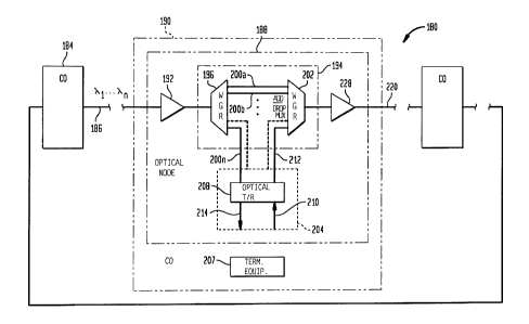
FIG. 4 shows an optical node/ring configuration 180 according to the
principles of the present
invention. A CO 184 provides optical signals having a plurality of wavelengths
~.,...~," along optical fiber
path 186 to an addldrop node I 88. The add/drop node 188 is representative of
one of a numbs of nodes that
can form the ring 180. The node 188 may or may not be part of a CO 190 shown
in dashed lines. At the
node 188, the optical signals on path 18G are amplified by pre-amplifier 192
(optional). In this particular
CA 02244385 1998-07-27
-5-
embodiment, an optical add/drop multiplexer 194 uses wavelength selection
devices, such as WGR 196 to
divide the optical signals by wavelength onto paths 200a - 200n, several of
which are directed to a WGR
202. The add/drop multiplexer 194 also drops one or more of the paths 200 to
optical transceiver circuitry
204, which can include one or more optical transceivers corresponding to
particular wavelengths (or
wavelength bands).
In this particular embodiment, an optical transceiver 208 receives an incoming
optical signal of a
particular wavelength (or wavelength bands) from the path 200n. If incoming
user informatian intended for
dropping at the node 188 is modulated onto the optical signal, the optical
transceiver 208 can retrieve the
downstream user infownation onto the path 214 to terminal equipment 209. The
optical transceiver 208
outputs an outgoing optical signal at the particular wavelength onto path 212
to the WGR 202 from at least a
portion of the light from the received optical signals. In doing so, the
optical transceiver 208 cen receive an
optical signal at the particular wavelength and modulate upstream user
information provided by the terminal
equipment 209 on line 210 onto the light of the optical signals for
transmission. The optical transceiver 208
can also output incoming optical signals bearing inform~adon intended for
othtr nodes without modulating
upstream user information onto the incaxning optical signals. Depending on the
particular embodiment, the
optical transceiver 208 can modulate the portion of light from incoming
optical signals bearing information
after the information on the light is suppressed.
The terminal equipment 209 can include processing circuitry to provide control
signals to the
optical transceiver circuitry 204 depending on the desigd and/or the optical
signal. For example, incoming
user information destined for multiple locations could be treated differently
by the optical transceiver, and/or
downstream control information could control the receiving of downstream user
information and the
modulating of outgoing user information by the optical transceiver 208. As
such, the optical transceiver 208
may or may not retrieve incoming user information and may or may not modulate
outgoing ustr information
onto the optical signal depending on the design and/or the type of information
in the optical signal. At the
add/drop multiplexer 194, the WGR 202 combines the optical signal of the
particular wavelength with the
optical signals at the other inputs of W(~R 202 to form a WDM signal on path
220. An amplifier 222, such
as an EDFA, can be used to amplify the optical signals comprising the WDM
signal,
The optical transceiver 20>s can be configured In various ways to maintain
light of a particular
wavelength flowing through the ring without the need for an optical source
tuned to the particular
wavelength at every node where that wavelength is dropped. The optical
transceiver accomplishes this by
receiving at least one incoming optical signal of at least one particular
wavelength and using at least a
portion of the light from the incoming optical signal for transmission. The
optical transceiver can output an
outgoing optical signal using the same incoming optical signal or an optical
signal of the same wavelength
from at least a portion of the light of the incoming optical signal which has
been altered and/or modulated
CA 02244385 1998-07-27
-6-
with outgoing user information. As such, the node according to the principles
of the present invention
enables a ring architecture with continuous or non-terminating optical paths
(i.e., optical paths do not end at
an electrical path) of particular wavelengths. Such an optical ring
architecture resulting from the optical
node system provides a cost incentive for using optical local loops or optical
distribution systems by
reducing the need and costs associated with conventional electrical ttrminal
equipment or optical/electrical
conversion equipment. An optical local loop system is disclosed in U.S. Patent
No. 5,559,624 to Darcie et
al" herein incorporated by reference.
FIG. 5 shows a block diagram of an embodiment of the an optical transceiver
208 for use in a node
configuration according to the principles of the present invention. In one
version of this partictalar
embodiment, an incoming optical signal at a particular wavelength on the path
202n includes information
intervals or "blank optical chalkboard" intervals or portions, the light of
which is used as a carrier for
outgoing information. In general, the blank optical cha~cboard refers to an
incoming optical signal with no
incoming information. The optical transceiver 208 receives the incoming
optical signal, and during the data
or incoming information intervals of the incoming optical signal, the
coupler/modulator 230 cauples the
incoming optical signals to a receiver 232. The receiver 232 neceives the
incoming optical signals and
extracts modulated data from the optical signals when there is incoming
information to be dropped. In one
particular embodiment, the receiver 232 converts the m4dulatod data into
electrical data signals which are
provided to the terminal equipment 209. In such an embodiment, the receiver
232 can employ any well
known type of optical receiver capable of receiving the tDptical signal from
path 202n and converting it to an
electrical signal.
The coupler/modulator 230 can also route the incoming optical signal towards
the path 212. In one
particular embodiment, during the optical chalkboard intervals of the optical
signal, the coupler/modulator
230 modulates outgoing user informati~ from the terminal equipment 209 onto
the lfght of the incoming
optical signal according to signal and control circuitry 234. As such, the
coupler/modulator 234 obtains
optical signals having a particular wavelength and modulates outgoing
information onto at least a portion of
the light from the incoming optical signsls for transmission as outgoing
optical signals onto the path 212.
Alternative embodiments for the optical transceiver and node configuration are
possible. For
example, in one version, the coupler/modulator 230 routes all of the incoming
optical signals to the receiver
232 during the data interval of the optical signal as controlled by the signal
and control circuitry 234. During
the optical chalkboard interval, the co~ler/modulator 230 routes all of the
incoming optical signals towards
the path 212, and the couplerlmodulator 230 modulates outgoa~g information
onto the optical signal for
transmission onto the path 212. As such, the signal and control circuitry 234
receives information from the
terminal equipment 209 as to when the incoming optical signal includes
incoming data or information to be
CA 02244385 1998-07-27
_7_
dropped and when the optical signal includes the optical chalkboard for
modulation of outgoing information,
which could be identical to the incoming user information.
FIG. 6 shows another version of the optical transceiver 208. The
coupler/modulator 230 includes a
coupler 240. The coupler 240 routes at least a portion of the downstream
optical signal (for example, 10%)
to the receiver 232 and the remaining portion (for example, 90%) is coupled on
a path 250 to a modulator
244. In this particular embodiment, the receiver 232 extracts the incoming
information from the portion of
the incoming optical signal which is coupled onto the path 245 by the coupler
240. Depending on the
particular embodiment and the electrical signals provided by the signal and
control circuitry 234, the
remaining portion of the optical signal can be either passed on to the path
212 without modulation, or if the
transmission of outgoing information is desired, the modulator 244 modulates
the remaining portion of the
incoming optical signal with the outgoing information to form the outgoing
optical signal. Thd outgoing
optical signal can be amplified with optional amplifier 222 (FIG. 4) if
necessary.
Thus, this embodiment enables incoming data to be obtained by the receiver 232
while providing an
optical signal at a particular wavelength for modulation and/or transmission
without delay. If the incoming
optical signal is to be forwarded to other destinations, the signal and
control circuitry 234 can provide control
signals to the modulator 244 and to signal conditioning circuitry 248
(optional, depending on die
embodiment) so that the incoming optical signal is not altered. As such, the
incoming optical signal can
continue flowing on the ring without interruption. In certain embodiments, if
at least a portion of the
incoming optical signal which has been modulated with incoming user
information on the path 250 is to be
used for modulation and transmission of outgoing user information, the signal
and control circuitry 234
provides control signals to the signal conditioning circuitry 248.
In certain embodiments, the signal conditioning circuitry 248 effectively
counteracts, rcmoves,
suppresses and/or attenuates the modulated portion of the incmning optical
signal. In this particular
embodiment, the signal conditioning circuit 248 includes a series of optical
amplifiers (not shaven) operating
in saturation as will be discussed below. T'he signal conditioning circuitry
248 outputs a relatively
unmodulated optical signal of the particular wavelength on the path 250 to the
modulator 244. If the
incoming optical signal includes an optical chalkboard interval or if other
nodes on the ring era to receive the
incoming information dropped at the receiver 232, the signal conditioning of
the incoming optical signal
may not be necessary, and the incoming optical signal could be provided
directly to the modulator 244. The
optical transceiver 208 can determine the presence of a blank optical
chalkboard interval by receiving
incoming information to signal the start of the blank optical chalkboard. The
modulator 244 modulates the
optical signal on the path 250 with outgoing user information as provided and
controlled by the signal and
control circuitry 234. In this description, modulation can include gain. The
modulator 244 can include a
LiNb03 modulator manufactured by Lucent Technologies, Inc., Murray Hill, N.
J., for example. The
CA 02244385 1998-07-27
_g_
modulator 244 transmits the outgoing modulated optical signals along the path
212 at the appropriate
wavelength for the WGR 202 (FIG. 4) to be combined with the other optical
signals on the path 220 (FIG.
4).
In certain embodiments such as those embodiments where the incoming optical
signal having
incoming information to be dropped is also to be used for modulation and
transmission of outgoing user
information, the signal conditioning circuitry 248 can b~ used to suppress the
modulated portion of the
incoming optical signal. FIG. 7 shows an embodiment of signal conditioning
circuitry 248. In this particular
embodiment, the signal conditioning circuitry 248 includes a plurality of
optical signal amplifier circuits 255,
257 and 259 connected In series. In this particular embodiment, the amplifier
circuits 255, 257 and 259 can
operate in their saturation range. When operating in the saturation range,
each amplifier stage of the signal
conditioning circuit 248 attenuates the modulated portion of the incoming
optical signal. Altet~natively, feed
forward techniques could be used to control the gains of the amplifier
circuits 255, 257 and 259. Such
techniques may require that some level of light be present at all time (i.e.
contrast ratio <1).
FIGs.8a-8d show how one embodiment of the signal conditioning circuitry 248
suppresses the
modulated portion of the incoming optical signal at each amplifier stage. FIG.
8a shows the incoming
optical signal modulated with incoming information at tie input to the signal
conditioning circuitry 248.
FIG. 8b shows the incoming optical signal being suppressed aRer passing
through the amplifier circuit 255,
and FIG. 8c shows the incoming optical signal being further suppressed after
passing through the amplifier
circuit 257. Finally, FIG. 8d shows the incoming optical signal after passing
through the amplifier circuit
259. By providing several stages of optical amplifiers operating in satur~ion,
it is possible to suppress or
effectively remove the modulated portion of the incoming optical signal. Of
course, the optical signral can be
passed through more or fewer
optical amplifiers, as necessary, to remove as much of the modulated portion
of the signal as desired. For
example, it may be possible to sufficiently suppress the modulated portion of
the optical signal using only
one or two optical amplifiers. On the other hand, it may be desirable to more
gradually suppress the optical
signal using more than three optical amplifiers. Alternatively, depending on
the application, the signal
conditioning circuitry 248 can be configured so that control signals can
enablt/disable the signal
conditioning circuitry 248 or change the operation of thd amplifier circuits
255, 257 and 259. For example,
depending on the embodiment and/or the incoming optical signal, the amplifier
circuits could be designed to
operate in saturation or not.
Accordingly, the present invention provides a system that obviates the need
for providing individual
laser light sources for each wavelength dropped or routed within each node to
the optical transceiver
according to the principles of the preset invention, thus simplifying the
structure, reducing overall cost and
reducing the amount of maintenance of the entire ring architecture. In certain
embodiments, the periodic
CA 02244385 1998-07-27
-9-
properties of the WGR can be used to allow light of additional wavelengths
spaced by multiples of the free
spectral range (FSR) to be used without additional optical circuitry, thereby
providing flexibility and the
potential for increased capacity. For example, a WGR could route optical
signals having wavelengths of ~,,
and ~, together as well as A,Z and 7~,"+~ together and so on. Additionally,
the node configuration according to
the principles of the present invention can quite efficiently accommodate
optical distribution systems,
thereby further reducing costs by alleviating the need far electrical terminal
equipment.
Alternative configurations of the node configuration according to the
principles of the present
invention are possible which omit or add components, use different schemes
depending upon the type of
incoming optical signals or control information in the incoming optical
signals and/or perform variations of
the above-described optical transceiver and control thereof. Other alternative
embodiments can be used
which are encompassed by the principles of the present invention to provide
continuous paths for certain
wavelengths of optical signals to reduce the need for optical sources
producing light at those wavelengths in
a ring architecture.
Furthermore, the node configuration has been described as being comprised of
several simple
components, but it should be understood that the node configuration and
portions thereof can be employed
using other forms of wavelength selection devices, add~'drop multiplexers and
variations in the configuration
of the optical transceiver. For example, FIG. 9 shows an altemativ.~
'embodiment for the optical node system
which uses a different configuration for the optical addJdrop multiplexes 280
than was used for the add/drop
multiplexes l94 (FIG. 4). The addldrop multiplexes 28~ includes a single
wavelength selection device, such
as a 2 X 2n WGR 282 which is shown having twice as many output poets when
compared to a previous
WGR described above. The WGR 282 receives optical signals having a plurality
of wavelengths ~., ..7.o from
the line 286. In this particular embodiment, by coupling pairs 288a-c of ports
together in a variety of
schemes taking into account channel spacing and interference, optical signals
having certain wavelengths ~.,
..A,3 are output onto line 290 for transmission onto the ring 292. In this
particular embodiment, incoming
optical signals having a wavelength 7v," are routed over lime 294 to optical
transceiver circuitry 29G which
includes optical transceiver 298. The optical transceiver 298 uses at least a
portion of the light from the
incoming optical signal to output an outgoing optical signal having the
wavelength A,, onto line 300 to the
WGR 282. The WGR 282 outputs the outgoing optical signal onto line 290 for
transmission over the ring
292.
The optical ring network architecture of the central ot~ices described above
which employs the
optical node system according to the principles of the present invention is
merely illustrative, and the node
configuration can be used in other optical ring architectures. Additionally,
the node configuration according
to the principles of the present invention can be implemented utilizing
various combinations of application
specific, optical and opto-electronic integrated circuits, software driven
processing circuitry, or other
CA 02244385 1998-07-27
-10-
arrangements of discrete components. What has been described is merely
illustrative of the application of
the principles of the present invention. Those skilled in the art will readily
recognize that these and various
other modifications, arrangements and methods can be made to the present
invention without strictly
following the exemplary applications illustrated and described herein and
without departing from the spirit
and scope of the present invention.