Note: Descriptions are shown in the official language in which they were submitted.
CA 02250504 2005-06-08
MULTIBIT SINGLE CELL MEMORY HAVING TAPERED CONTAGT
FIELD OF THE INVENTION
The present invention relates generally to a uniquely designed solid state,
electrically and optically operated, directly overwritable, low energy, very
fast switching,
non-volatile, analogue and multilevel single-cell operating memory element,
and to high
density electrical memory arrays fabricated from these elements. More
specifically, the
present invention relates to a memory element having a tapered contact layer.
BACKGROUND AND PRIOR ART
The Ovonic EEPROM is a novel, proprietary, high performance, non-volatile,
thin-film electronic memory device. Its advantages include non-volatile
storage of data,
potential for high bit density and, consequently, low cost because of its
small footprint and
simple two-terminal device configuration, long reprogramming cycle life, low
programming
energies and high speed. The Ovonic EEPROM is capable of both analog and
digital
forms of information storage. Digital storage can be either binary (one bit
per memory cell)
or multi-state (multiple bits per cell). Only minor modifications are
necessary to switch
between the two digital modes. For purposes of the instant invention, the
terms "memory
elements" and "control elements" will be employed synonymously.
EARLY ELECTRICAL PHASE CHANGE MEMORY
The general concept of utilizing electrically veritable and erasable phase
change
materials (i.e., materials which can be electrically switched between
generally amorphous
and generally crystalline states) for electronic memory applications is well
known in the
art, as is disclosed, for example, in U.S. Patent No. 3,271,591 to Ovshinsky,
issued
September 6, 1996 and in U.S. Patent No. 3,530,441 to Ovshinsky, issued
September 22,
1970, both of which are assigned to the same assignee as the present invention
(hereinafter the "Ovshinsky patents").
As disclosed in the Ovshinsky patents, such phase change materials can
CA 02250504 1998-09-29
WO 97/40499 PCT/US97/06538
2
be electrically switched between structural states of generally amorphous and
generally crystalline local order or between different detectable states of
local order
across the entire spectrum between completely amorphous and completely
crystalline states. That is, the Ovshinsky patents describe that the
electrical
switching of such materials is not required to take place between completely
amorphous and completely crystalline states but rather can be in incremental
steps
reflecting changes of local order to provide a "gray scale" represented by a
multiplicity of conditions of local order spanning the spectrum between the
completely amorphous and the completely crystalline states. The early
materials
described by the Ovshinsky patents could also, if required, be switched
between
just the two structural states of generally amorphous and generally
crystalline local
order to accommodate the storage and retrieval of single bits of encoded
binary
information.
In the typical personal computer there are often four tiers of memory.
Archival information is stored in inexpensive, slow, high storage capacity,
non-
volatile devices such as magnetic tape and floppy disks. This information is
transferred, as needed, to faster and more expensive, but still non-volatile,
hard
disk memories. Information from the hard disks is transferred, in turn, to the
still
more expensive, faster, volatile system memory which uses semiconductor
dynamic RAM (DRAM) devices. Very fast computers even transfer forth and back
small portions of the information stored in DRAM to even faster and even more
expensive volatile static RAM (SRAM) devices so that the microprocessor will
not
be slowed down by the time required to fetch data from the relatively slower
DRAM. Transfer of information among the tiers of the memory hierarchy occupies
some of the computer's power and this need for "overhead" reduces performance
- - and results in additional complexity in the computer's architecture. The
current use
of the hierarchai structure, however, is dictated by the price and performance
of
available memory devices and the need to optimize computer performance while
minimizing cost.
The electrically erasable phase change memories described in the
Ovshinsky patents, as well as subsequent electrical solid state memory, had a
number of limitations that prevented their widespread use as a direct and
universal
CA 02250504 1998-09-29
WO 97140499 PCT/US97/06538
3
replacement for present computer memory applications, such as tape, floppy
disks,
magnetic or optical hard disk drives, solid state disk flash, DRAM, SRAM, and
socket flash memory. Specifically, the following represent the most
significant of
' these limitations: (i) a relatively slow (by present standards) electrical
switching
speed, particularly when switched in the direction of greater local order (in
the
direction of increasing crystallization); (ii) a relatively high input energy
requirement
necessary to initiate a detectable change in local order; and (iii) a
relatively high
cost per megabyte of stored information {particularly in comparison to present
hard
disk drive media).
The most significant of these limitations is the relatively high energy input
required to obtain detectable changes in the chemical and/or electronic
bonding
configurations of the chalcogenide material in order to initiate a detectable
change
in local order. Also significant were the switching times of the electrical
memory
materials described in the Ovshinsky patents. These materials typically
required
times in the range of a few milliseconds for the set time (the time required
to
switch the material from the amorphous to the crystalline state); and
approximately
a microsecond for the reset time {the time required to switch the material
from the
crystalline back to the amorphous state). The electrical energy required to
switch
these materials typically measured in the range of about a microjoule.
It should be noted that this amount of energy must be delivered to each of
the memory elements in the solid state matrix of rows and columns of memory
cells. Such high energy levels translate into high current carrying
requirements for
the address lines and for the cell isolationladdress device associated with
each
discrete memory element. Taking into consideration these energy requirements,
the choices of memory cell isolation elements for one skilled in the art would
be
. - limited to very large single crystal diode or transistor isolation
devices, which would
make the use of micron scale lithography and hence a high packing density of
memory elements impossible. Thus, the low bit densities of matrix arrays made
from this material would result in a high cost per megabyte of stored
information.
By effectively narrowing the distinction in price and performance between
archival, non-volatile mass memory and fast, volatile system memory, the
memory
elements of the present invention have the capability of allowing for the
creation
CA 02250504 1998-09-29
WO 97/40499 PCT/US97/06538
4
of a novel, non-hierarchal "universal memory system". Essentially all of the
memory in the system can be low cost, archival and fast. As compared to
original
Ovshinsky-type phase change electrical memories, the memory materials
described
herein provide over six orders of magnitude faster programming time (less than
30
nanoseconds) and use extremely low programming energy (less than 0.1 to 2
nanojoules) with demonstrated long term stability and cyclability (in excess
of 10
trillion cycles). Also, experimental results indicate that additional
reductions in
element size can increase switching speeds and cycle life.
In general, development and optimization of the class of chalcogenide
memory materials has not proceeded at the same rate as other types of solid
state
electrical memories that now have substantially faster switching times and
substantially lower set and reset energies. These other forms of memories
typically employ one or two solid state microelectronic circuit elements for
each
memory bit (as many as three or four transistors per bit) in some memory
applications. The primary "non-volatile" memory elements in such solid state
memories, such as EEPROM, are typically floating gate field effect transistor
devices which have limited re-programmability and which hold a charge on the
gate
of a field effect transistor to store each memory bit. Since this charge can
leak off
with the passage of time, the storage of information is not truly non-volatile
as it
is in the phase change media of the prior art where information is stored
through
changes in the actual atomic configuration or electronic structure of the
chalcogenide material from which the elements are fabricated. These other
forms
of memories now enjoy acceptance in the marketplace.
In contrast to DRAM and SRAM, volatile memory devices, and other "flash"
devices such as floating gate structures, no field effect transistor devices
are
- - required in the electrical memory devices of the present invention. In
fact, the
electrically erasable, directly overwritable memory elements of the present
invention represent the simplest electrical memory device to fabricate,
comprising
only two electrical contacts to a monolithic body of thin film chalcogenide
material
and a semiconductor diode for isolation. As a result, very little chip "real
estate"
is required to store a bit of information, thereby providing for inherently
high density
memory chips. Further, and as described below, additional increases in
CA 02250504 1998-09-29
WO 97/40499 PCT/US97/06538
information density can be accomplished through the use of multibit storage in
each discrete memory cell.
The solid state, electronic memories presently in use are relatively
expensive to manufacture, the cost being typically about eighty times the cost
per
5 bit of storage capacity in relation to magnetic disk storage. On the other
hand,
these solid state, electronic memories provide certain advantages over
magnetic
disk memories in that they have no moving parts, require less electrical
energy to
operate, are easy to transport and store, and are more versatile and adaptable
for
use with portable computers and other portable electronic devices. As a matter
of
fact, hard drive manufacturers are forecasting rapid growth in the use of ever
smaller hard drives and eventually solid state memory storage in the portable
computer field. in addition, these solid state memories are usually true
random
access systems as opposed to disk types which require physical movement of the
disk head to the proper data track for accessing the desired memory location.
However, in spite of such advantages, the higher cost of solid state
electrically
erasable memories have prevented them from enjoying a substantial share of the
market now dominated by magnetic memory systems. Although solid state
electrically erasable memories could potentially be manufactured at reduced
cost,
the overall price-to-performance ratio of these devices is inadequate for them
to
fully replace magnetic disk systems.
A recently developed memory device is the metal-amorphous silicon-metal
(MSM) electrical memory switch. See Rose, et al, "Amorphous Silicon Analogue
Memory Devices", Journal of Non-Crystalline Solids, 115(1989), pp.168-70 and
Hajto, et al, "Quantized Electron Transport in Amorphous -Silicon Memory
Structures", Physical Review Letters, Vo1.66, No. 14, April 8, 1991, pp. 1918-
21.
- This MSM switch is fabricated by the deposition of specifically selected
metallic
contacts on either side of a p-type amorphous silicon (a-Si) thin film. The
importance of the selection of the metallic contact materials will be
discussed later.
MSM memory switches are disclosed as exhibiting relatively fast (10-100 ns)
analogue switching behavior for voltage pulses of from 1-5 volts, thereby
providing
a range of resistances of from about 103 to about 106 ohms to which they can
be
set in a non-volatile manner. As should be readily apparent to skilled
practitioners
CA 02250504 1998-09-29
WO 97!40499 PCT/US97106538
6
in the art, the MSM memory switches of Rose, et al and Hajto, et al, although
exhibiting electrical switching characteristics (i.e.,times, energies and
resultant
device resistance) similar to the electrical switching characteristics of the
memory
elements of the instant invention, there are actually significant operational
differences therebetween.
The most significant electrical switching difference resides in the inability
of
the MSM memory switches to be directly overwritten. That is, the MSM switches
cannot be modulated directly bidirectionally from any one resistance in the
analogue range of resistances to any other resistance in that range without
first
being erased (set to a specific starting resistance or "starting state"). More
specifically, the MSM switch must first be set to the high resistance state
(erased)
before said switch can be set to another resistance value within the analogue
range. In contrast thereto, the memory elements of the instant invention do
not
require erasure before being set to another resistance in the range; i.e.,
they are
directly overwritable.
Another significant difference in the electrical switching characteristics
which
exists between the MSM memory switches of Rose, et al and Hajto, et al and the
electrical memory elements of the present invention is the bipolar behavior of
the
MSM switches. As is disclosed by Rose, et al, the MSM switches must be erased
using electrical pulses of reverse polarity from those pulses used to write.
Significantly, this reversal of polarity of the applied pulse is not required
by the
memory elements of the present invention, whether the instant memory elements
are used for digital or analogue switching.
These differences in electrical switching characteristics between the MSM
switches and the memory elements of the present invention are attributable to
- more than just a mere difference in material from which the elements are
constructed. These differences are indicative of the fundamental differences
in
switching mechanisms which characterize the physics of operation of the two
devices. As alluded to above and as disclosed in the aforementioned articles,
the
electrical switching characteristics of the MSM memory switches are critically
dependent upon the particular metals) from which the contacts are fabricated.
This is because these MSM switches require a very highly energetic "forming"
CA 02250504 1998-09-29
WO 97!40499 PCT/US97/06538
7
process in which metal from at least one of the contacts is transported into
and
formed as an integral portion of the switch body. In this process, a plurality
(at
least 15 from Fig. 1 of the Rose, et al paper) of progressively increasing 300
nanosecond, 5-15 volt pulses are employed to form the switch. Rose, et al
state:
"...X-ray microanalysis studies of the devices have been carried out, and the
top
electrode material has been found embedded in a filamentary region of the a-
Si.
This suggests that the top metal becomes distributed in the filament, and may
play
a role in the mechanism of switching. ..." Rose, et al also specifically find
that the
dynamic range of the available resistances is determined by the metal from
which
the upper electrode contact is fabricated. As is stated by Rose, et al: ...it
is found
that its value is entierly (sic) dependent on the top contact, and completely
independent of the bottom metallisation (sic), i.e. Cr top electrode devices
are
always digital and V top electrode devices are always analogue irrespective of
the
bottom electrode. It is within this metallic filamentary region where the
electrical
switching occurs; and without this mass migration of metal into the a-Si,
there
would be no switching, see the Hajto, et al paper. In complete
contradistinction
thereto, the memory elements of the present invention do not require migration
of
the contact material into the thin-film memory element to achieve high speed,
low
energy, analogue, direct overwrite, memory switching. As a matter of fact, in
the
fabrication of the memory elements of the instant invention, great care is
taken to
prevent diffusion of metal from either of the electrodes into the active
chalcogenide
- material.
From the foregoing analysis of Rose, et al and Hajto, et al, it should be
clear
that MSM memory switches do not, by any stretch of the imagination qualify as
a
modulator of free charge concentration. Rather, MSM memory switches simply
_ rely upon the creation of a filamentary metallic pathway through the
amorphous
silicon material in order to obtain a range of resistivities in much the same
way as
a modulated switch is used to control the flow of electrical current. A
percolation
pathway is established, the diameter of which can be increased or decreased to
change the resistivity thereof. No movement of Fermi level position is
involved in
the switching process. No change in activation of the semiconductor material
need
be invoked to explain the operation. No atomic scale movement of lone pairs of
CA 02250504 1998-09-29
WO 97/40499 PCT/US97/06538
8
non-bonding electrons is present. Crystallite size and surface to volume ratio
thereof is not important. But most importantly, it is impossible for Rose, et
al and
Hajto, et al to directly overwrite information stored in the cells of their
memory
material. The MSM switch requires stored information to be erased before new
information can be written. It is not surprising that Rose, et al have
asserted that
their MSM switch is limited to one million cycles while the memory elements of
the
instant invention were cycled over 10 trillion cycles without failure prior to
ending
the test.
Simply stated, no solid state memory system developed prior to the present
invention, regardless of the materials from which it was fabricated, has been
inexpensive; easily manufacturable; non-volatile; electrically writable and
directly
erasable (overwritable) using low input energies; capable of multibit storage
in a
single cell (had a gray scale); and capable of very high packing density. The
memory system described hereinbelow, because it addresses all of the
deficiencies
of known memory systems, will find immediate widespread use as a universal
replacement for virtually all types of computer memory currently in the
marketplace.
Further, because the memories of the present invention can be fabricated in an
all
thin-film format, three-dimensional arrays are possible for high speed, high
density
neural network, and artificial intelligence applications. The memory system of
the
present invention is therefore uniquely applicable to neural networks and
artificial
intelligence systems because its multi-layer, three-dimensional arrays provide
massive amounts of information storage that is rapidly addressable, thus
permitting
learning from stored information.
It is clear from the discussion above that the quantitative changes in
switching speed and energy requirements of the memories of the present
invention,
as compared to the phase change memories of the prior art, demonstrate that
those memories define an entirety new class of modulatable semiconductor
material. In addition, the prior art has no analog to the direct overwrite,
wide
dynamic range and multibit storage capabilities of the instant memory
elements.
As should be abundantly clear to ordinarily skilled artisans, in order to
address the flash EEPROM market and be seriously considered as a universal
memory, it is essential that memory elements be truly non-volatile. This is
even
CA 02250504 1998-09-29
WO 97/40499 PCT/CTS97106538
9
more significant if the memory element is claimed to possess multibit storage
capabilities. If a set resistance value is lost or even found to significantly
drift over
time, the information stored therein is destroyed, users lose confidence in
the
archival capabilities of the memory and the technology loses all credibility.
In addition to set resistance stability, another highly important factor which
would be required of a universal memory is low switching current. This is
extremely significant when the EEPROMs are used for large scale archival
storage.
Used in this manner, the EEPROMs would replace the mechanical hard drives
(such as magnetic or optical hard drives) of present computer systems. One of
the
main reasons for this replacement of conventional mechanical hard drives with
EEPROM "hard drives" would be to reduce the comparatively large power
consumption of the mechanical systems. In the case of lap-top computers, this
is
of particular interest because the mechanical hard disk drive is one of the
largest
power consumers therein. Therefore, it would be especially advantageous to
reduce this power load, thereby substantially increasing the usage time of the
computer per charge of the power cells. However, if the EEPROM replacement
for mechanical hard drives has high switching energy requirements (and
therefore
high power requirements), the power savings may be inconsequential or at best
unsubstantial. Therefore, any EEPROM which is to be considered a universal
memory requires low switching energy.
Yet another requirement of a EEPROM universal memory is high thermal
- stability of the information stored therein. Today's computers, especially
personal
computers, are routinely subjected to high temperatures. These high
temperatures
can be caused by internally created heat such as from power sources or other
heat
producing internal components. These high temperatures may also be caused by
environmental factors, such as use of the computer in a hot climate or storage
of
the computer in an environment which is directly or indirectly heated to
higher than
normal temperatures. Whatever the cause of the elevated temperatures, present
computer memory systems, especially "hard" or archival memory, must be
thermally stable even at relatively high temperatures. Without this thermal
stability
data loss may occur leading to the aforementioned loss of credibility.
Still another requirement of a EEPROM universal memory is long
CA 02250504 1998-09-29
WO 97/40499 PCT/US97/06538
write/erase cycle life. For EEPROMs, as is the case with all archival memory,
cycle life plays an important role in consumer confidence and acceptance. If
the
cycle life of a memory device is too short, the consumer will be adverse to
using
this device for fear of losing valuable data. If the EEPROM is to be used as a
5 replacement for computers main memory or display memory, that is, as a
replacement for DRAM, SRAM or VRAM, the requirement of long cycle life is even
more critical. The main and display memory are a computer's most often written
tolerased data storage area. Every time a new computer program is loaded, a
portion of the computer's main memory is erased and rewritten. During the
10 execution of a computer program, a portion of the computer's main memory is
constantly being cycled. Every time the computer monitor's display is changed,
portions of the display memory are cycled. If the EEPROMs used to replace the
computer's main and display memory do not have a relatively long write/erase
cycle life, these memories would need to be replaced excessively. This would
lead
to excessive costs to the consumer and therefore loss of consumer confidence.
SUMMARY OF THE INVENTION
There is disclosed herein an electrically operated, directly overwritable,
multibit, single-cell memory element comprising a volume of memory material
defining a single cell memory element, the memory material characterized by (1
)
a large dynamic range of electrical resistance values, and (2) the ability for
at least
a filamentary portion of the memory material to be set to one of a plurality
of
resistance values within the dynamic range in response to selected electrical
input
signals so as to provide the single-cell memory element with multibit storage
capabilities. At least a filamentary portion of the single cell memory element
being
setable, by the selected electrical signal to any resistance value in the
dynamic
range, regardless of the previous resistance value of the material.
The memory element further comprises a first spacedly disposed contact for
supplying the electrical input signal to set the memory material to a selected
resistance value within the dynamic range, and a second spacedly disposed
contact for supplying the electrical input signal to set the memory material
to a
selected resistance value within the dynamic range, the second contact
tapering
CA 02250504 1998-09-29
WO 97/40499 PCT/US97106538
11
to a peak adjacent to the memory element, the peak defining the size and
position
of the filamentary portion during electrical formation of the memory element.
BRIEF DESCRIPTION OF THE DRAWINGS
Fig. 1 is a cross-sectional view of a single memory element depicting a
second contact that tapers to a peak adjacent to the memory material;
Fig. 2 is a cross-sectional view of a single memory element depicting a
second contact comprising an additional thin-film layer of carbon material;
Fig. 3 is the top view of a possible layout of multiple memory elements
showing how the elements would be connected to a set of X-Y addressing lines;
Fig. 4 is a schematic diagram of the memory elements from Fig. 1 showing,
in addition, how isolation elements such as diodes are connected in series
with the
memory elements to electrically isolate each of the devices from the others;
Fig. 5 is a schematic representation illustrating a single crystal
semiconductor substrate with the integrated memory matrix of the instant
invention
as depicted in Fig. 1 placed in electrical communication with an integrated
circuit
chip on which the addressldrivers/decoders are operatively affixed;
Fig. 6 is a ternary phase diagram of the Ge:Sb:Te alloy system from which
the memory elements of the instant invention are fabricated, said phase
diagram
showing some of the multiple phases into which various mixtures of these
elements segregate upon rapid solidification.
DETAILED DESCRIPTION OF THE INVENTION
Erasable electrical memories fabricated from the broad class of
chalcogenide materials have employed structural changes that were
_ _ accommodated by movement of certain atomic species within the material to
permit change of phase as the material switched from the amorphous state to
the
crystalline state. For example, in the case of electrically switchable
chalcogenide
alloys formed of tellurium and germanium, such as those comprising about 80%
to 85% tellurium and about 15% germanium along with certain other elements in
small quantities of about one to two percent each, such as sulfur and arsenic,
the
more ordered or crystalline state was typically characterized by the formation
of a
CA 02250504 1998-09-29
WO 97/40499 PCT/US97/06538
12
highly electrically conductive crystalline Te filament within the switchable
pore of
the memory material. A typical composition of such a prior art material would
be,
for example, Te8,Ge,5S2As2 or TeB~Ge,SSzSbz. Because Te is so highly
conductive
in its crystalline state, a very low resistance condition was established
through the
Te filament in the more ordered or crystalline state; this resistance being a
number
of orders of magnitude lower than the resistance of the pore in the less
ordered or
amorphous state.
However, the formation of the conductive Te filament in the crystalline state
required migration of the Te atoms from their atomic configuration in the
amorphous state to the new locally concentrated atomic configuration in the
crystalline Te filament state. Similarly, when the chalcogenide filamentary
material
was switched back to the amorphous state, the Te which had precipitated out
into
the crystalline filament was required to migrate within the material from its
locally
concentrated form in the filament back to its atomic configuration in the
amorphous
state. This atomic migration, diffusion or rearrangement between the amorphous
and crystalline states required in each case a holding or dwell time of
sufficient
length to accommodate the migration, thereby making the requisite switching
time
and energy relatively high.
The subject inventors have discovered a remarkable reduction in both the
required switching time and the energy input for a fundamentally different
type of
electrically erasable, directly overwritable memory based up on a new class of
chalcogenide semiconductor materials. Moreover, the chalcogenide materials
provides for switching within a wide dynamic range of stable states with
remarkably
low energy inputs at remarkably fast speeds so that this newly discovered
class
of materials can be used to fabricate improved electrical memory elements.
Specifically, the memory material can be switched between electrically
detectable conditions of varying resistance in nanosecond time periods (the
minimum switching speed and minimum energy requirements have not as yet been
ascertained, however, experimental data as of the filing of this application
have
shown that the electrical memory can be modulated (even though not optimized)
with as short as 1 nanosecond programming pulses) with the input of picojoules
of energy. This memory material is non-volatile and will maintain the
integrity of
CA 02250504 1998-09-29
WO 97/40499 PCT/US97/06538
13
the information stored by the memory cell (within a selected margin of error)
without the need for periodic refresh signals. In contrast to many other
semiconductor materials and systems heretofore specified for memory
applications,
the semiconductor memory material and systems of the present invention can be
directly overwritable so that the discrete memory elements need not be erased
(set
to a specified starting point) in order to change information stored there.
The
remarkably fast and low energy switching to any of the different values of
resistance can be attributed to the fact that said switching occurs without
the need
for gross atomic rearrangement of the switching material.
The memory material is formed from a plurality of constituent atomic
elements, each of which is present throughout the entire volume of memory
material. The plurality of constituent atomic elements preferably includes at
least
one chalcogen element and may include at least one transition metal element.
The term "transition metal" as used herein includes elements 21 to 30, 39 to
48,
57 and 72 to 80. More preferably, the plurality of constituent atomic elements
which form the volume of memory material includes elements selected from the
group consisting of Te, Se, Ge, Sb, Bi, Pb, Sn, As, S, Si, P, O and mixtures
or
alloys thereof. More preferably the transition metal includes Cr, Fe, Ni and
mixtures of alloys thereof and the chaicogen element includes Te and Se. Most
preferably the transition metal is Ni. Specific examples of such multi-element
systems are set forth hereinafter with respect to the Te:Ge:Sb system with or
without Ni and/or Se.
Regardless of the explanation of the manner in which programming is
accomplished, the present invention provides a combination of valuable
electrical
switching characteristics never before available in a single memory element.
_ The specific semiconductor alloys employed in fabricating the memory
devices include chalcogenide elements which are particularly noted for the
presence of "lone pair" electrons. It is therefore necessary to discuss the
effect of
those lone pair electrons in available chemical bonding configurations. Simply
stated, a lone pair is a pair of electrons in the valence shell of an atom
that is
typically not engaged in bonding. Such lone pair electrons are important both
structurally and chemically. They influence the shape of molecules and
crystalline
CA 02250504 1998-09-29
WO 97/40499 PCT/US97/06538
14
lattice structures by exerting strong repulsive forces on neighboring electron
pairs '
which are engaged in bonding configurations and as well as on other lone
pairs.
Since lone pair electrons are not tied down into a bonding region by a second
nucleus, they are able to influence and contribute to low energy electronic
transitions. As first pointed out by Ovshinsky, the lone pairs can have 1 and
3
center bonding; and as demonstrated by Kastner, Adler and Fritsche, they have
valance alternation pairs.
Specifically, the tellurium alloys described herein have a valence band made
up of lone pair states. Since four (4) p shell electrons are present in Te,
and the
Te atom is chemically bonded by two of these bonding electrons in the p shell,
the
other two outer electrons (the lone pair) are not utilized for bonding
purposes and
hence do not substantially change the atomic energy of the system. In this
regard,
note that the highest filled molecular orbital is the orbital which contains
the lone
pair electrons. This is significant because, in a perfect stoichiometric
crystal of
tellurium and germanium atoms, upon the application of some internal strain in
the
lattice from which the crystallite is formed, the valence band can broaden and
move upward toward the position of the then existing Fermi level. However,
TeGe
crystals are naturally "self-compensated", that is, the crystal desires to
preferentially assume a Te rich (approximately 52 percent Te and 48 percent
Ge)
composition. The stoichiometric crystal is a face centered cube; however, with
the
addition of a minimal amount of energy, the crystal can assume a rhombohedral
lattice structure by increasing the number of its Ge andlor Sb vacancies. It
is this
creation of vacancies in the crystalline lattice structure, which can reduce
lattice
strain in TeGe alloys, is responsible for lowering the energy state of the
material
and moves the Fermi level toward the valence band.
- It is acceptable, if not essential to superimpose an amorphous model of
local order on top of a short range local order model for the purpose of
obtaining
a descriptive, if not perfectly predictive explanation of atomic behavior.
When
considering the amorphous nature of the material, note that the density of
defect
states in the band tails is greatest adjacent the band edges, while the depth
of the
recombination centers for captured charge carriers are deeper farther away
from
the band edges. The presence of these deep traps and tail states would provide
CA 02250504 1998-09-29
WO 97/40499 PCT/LTS97/06538
a possible explanation for intermediate stable resistance values between the
Fermi
level position and the band edge. Regardless of theory, when fully
crystalline, the
semiconductor material of the instant invention is a degenerate semiconductor
which exhibits metallic-like conduction.
5 It is further believed that the size of the crystallites which exist in the
bulk
of the semiconductor and memory material is relatively small, preferably less
than
about 2000 ~, more preferably between about 50 ~ and 500 ~, and most
preferably
on the order of about 200 ~ to about 400 ~. Further, these crystallites are
believed
to be surrounded by an amorphous skin which may contribute to the rapid
10 formation of the many Fermi level positions of the material, detectable as
different
resistances (conductivities), as well as to the lower energy requirements for
the
transitions between these detectable resistance values to which the material
can
be reliably and repeatably set.
It has also been found that modulation of the switching characteristics of two
15 or three terminal semiconductor devices fabricated from the
microcrystalline
materials of the present invention may be controlled such that repeatable and
detectable resistance values can be effected. It has been found that, in order
for
the materials of the present invention to be quickly set by low energy input
signals
to a desired conductivity (determined by the Fermi level position), it is only
necessary that said materials are capable of stable (or long lived metastable)
existence within at least two different Fermi level positions, which Fermi
level
positions are characterized by substantially constant band gaps but different
electrical conductivities. As noted above, it is also believed that the
relatively small
crystallite size may contribute to the rapid transition between detectable
values of
resistance.
One characteristic of the semiconductor materials of the present invention
is their tendency toward the formation of more and smaller crystallites per
unit
volume. Crystallite sizes of the widest preferential range of representative
materials embodying the present invention have been found to be far less than
about 2000 ~, and generally less than the range of about 2,000 ~ to 5,000 ~
which
was characteristic of prior art materials. Crystallite size is defined herein
as the
diameter of the crystallites, or of their "characteristic dimension" which is
CA 02250504 1998-09-29
WO 97/40499 PCT/US97I06538
16
equivalent to the diameter where the crystallites are not spherically shaped.
It has been determined that compositions in the highly resistive state of the
class of TeGeSb materials which meet the criteria of the present invention are
generally characterized by substantially reduced concentrations of Te relative
to
that present in prior art electrically erasable memory materials. In one
composition
that provides substantially improved electrical switching pertormance
characteristics, the average concentration of Te in the as deposited materials
was
well below 70%, typically below about 60% and ranged in general from as low as
about 23% up to about 58% Te and most preferably about 48% to 58% Te.
Concentrations of Ge were above about 5% and ranged from a low of about 8%
to about 30% average in the material, remaining generally below 50%. Most
preferably, concentrations of Ge ranged from about 8% to about 40%. The
remainder of the principal constituent elements in this composition was Sb.
The
percentages given are atomic percentages which total 100% of the atoms of the
constituent elements. Thus, this composition may be characterized as
TeaGebSb~°°-ca+e~. These ternary Te-Ge-Sb alloys are useful
starting materials for
the development of additional memory materials having even better electrical
characteristics.
A ternary diagram of the Te:Ge:Sb system is shown in Fig. 6. Melts were
prepared from various mixtures of Te, Ge and Sb, the melts segregated into
multiple phases upon rapid solidification. Analysis of these rapidly
solidified melts
indicated the presence of ten different phases (not all present in any one
rapidly
solidified melt). These phases are: elemental Ge, Te and Sb, the binary
compounds GeTe, and Sb2Te3 and five different ternary phases. The elemental
compositions of all of the ternary phases lie on the pseudobinary GeTe-SbzTe3
fine
- - and are indicated by the reference letters A, B, C, D and E on the ternary
diagram
shown in Fig. 6. The atomic ratios of the elements in theses five ternary
phases
areset forth in Table 1. A more detailed description of Fig. 6 is presented
hereinbeiow
CA 02250504 1998-09-29
WO 97/40499 PCT/US97106538
17
Table 1
Observed Ternary Crystalline Phases of the TeGeSb SSrstem
Designation At ~ Ge At ~ Sb At o Te
A 40 10 50
B 26 18 56
C 18 26 56
D 14 29 57
E 8 35 56
The novel memory elements of the present invention include a volume of
memory material, said memory material preferably including at least one
chalcogen
and can include one or more transition metals. The memory materials which
include transition metals are elementally modified forms of our memory
materials
in the Te-Ge-Sb ternary system. That is, the elementally modified memory
materials constitute modified forms of the Te-Ge-Sb memory alloys. This
elemental modification is achieved by the incorporation of transition metals
into the
basic Te-Ge-Sb ternary system, with or without an additional chalcogen
element,
such as Se. Generally the elementally modified memory materials fall into two
categories.
The first category is a memory material which includes Te, Ge, Sb and a
- transition metal, in the ratio (TeaGebSb~°o-~a+b>)~TM,oo-~ where the
subscripts are in
atomic percentages which total 100% of the constituent elements, wherein TM is
one or more transition metals, a and b are as set forth herein above for the
basic
Te--Ge--Sb ternary system and c is between about 90% and about 99.99%. The
transition metal preferably includes Cr, Fe, Ni, Nb, Pd, Pt and mixtures or
alloys
thereof.
Specific examples of memory materials encompassed by this system would
include (TeSSGezzSbz2)9sNis, (TessGeZ2Sb2z)9oNi,o, (TeSSGezzSbZZ)ssCrs~
(TessC''ezzSbzz)s°Cr,o~ (Tesst''ezzSbzz)ssFes~
(Tess~''ezzSbzz)s°Fevo~ (TessGezZSbz2)ssPds,
(TessGe22Sbzz)soPd,o~(TessGezzSbzz)ssPts,
(TessGezzsb22)ssPtSO~(TessGezzsbzz)ssNbs~
(TessGezzSbzz)soNblo~ (TessGez2sbzz)soNisCrS, (TessGezzSbzz)soNisFes,
CA 02250504 1998-09-29
WO 97/40499 PCT/US97/06538
18
(TessGezzSbzz)soCrsFes~ (TessGezzsbzz)soPdsCrs~ (TessGezzsbzz)s°NisPds,
(TeSSGezzSbzz)s°PdsPts, etC.
The second category is a memory material which includes Te, Ge, Sb, Se
and a transition metal, in the ratio
(TeaGebSb,oo-ea+e~)~TMdSe,oo-~~+a~ where the subscripts are in atomic
percentages
which total 100% of the constituent elements, TM is one or more transition
metals,
a and b are as set forth hereinabove for the basic Te-Ge-Sb ternary system, c
is
between about 90% and 99.5% and d is between about 0.01 % and 10%. The
transition metal can preferably include Cr, Fe, Ni, Pd, Pt, Nb and mixtures of
alloys
thereof. Specific examples of memory materials encompassed by this system
would include (TessGezzSbzz)9oNi5Se5, (TessGezzSbzz)soNi,oSe,o,
(TessGe2zsbzz)s°CrsSeS, (TessGezzSbzz)soCr,°Se,o~
(TessGe22sbzz)s°FesSeSt
(TessGezzSbzz)s°Fe,°Se~o~ (TessGezzsbzz)s°PdsSes~
(TessGezzSb2z)s°Pd,°Se,°~
(TessGezzsbzz)s°PtsSes~ (TessGezzSbzz)aoPt,ose,°~
(TessGezzsbzz)soNbsSes,
(Te56Ge22Sb2z)s°NbloSeio, ~TessGezzSbzz)ssNisCr5Se5,
(TessGezzSbzz)aoN~sFeSSe~o,
(TessGe22sbzz)asCrsFe5Se5,
(TessGe22sbz2)asNisPd5Se5,(TessGezzsbzz)a°NisPtSSe,o,
~TessGezzsbzz)asNi~Nb5Se5, (TessGezzsb22)esPdsCr5Se5,
(TeSSGezzsbzz)soPdsPtSSe,o,
(Te56Ge22Sbzz)ssPdsNb5Se5, (Te56GeZZSbZZ)ssPtsNb5Se5, etc.
The memory elements ofthe instant patent application possess substantially
non-volatile set resistance values. However, if the resistance value of the
instant
memory elements does, under some circumstances, drift from its original set
value,
"compositional modification", described hereinafter, may be used to eliminate
for
this drift. As used herein, the term "non-volatile" will refer to the
condition in which
the set resistance value remains substantially constant for archival time
periods.
Of course, software (including the feedback system discussed hereinafter) can
be
. - employed to insure that absolutely no "drift" occurs outside of a selected
margin
of error. Because drift of the resistance value of the memory elements can, if
left
unimpeded, hinder gray scale storage of information, it is desirable to
minimize
drift.
"Compositional modification" is defined herein to include any means of
compositionally modifying the memory material to yield substantially stable
values
of resistance, including the addition of band gap widening elements to
increase the
CA 02250504 1998-09-29
WO 97/40499 PCT/US97/06538
19
inherent resistance of the material. One example of compositional modification
is
to include graded compositional inhomogeneities with respect to thickness. For
instances, the volume of memory material may be graded from a first Te-Ge-Sb
alloy to a second Te-Ge-Sb alloy of differing composition. The compositional
grading may take any form which reduces set resistance value drift. For
example,
the compositional grading need not be limited to a first and second alloy of
the
same alloy system. Also, the grading can be accomplished with more than two
alloys. The grading can be uniform and continuous or it can also be non-
uniform
or non-continuous. A specific example of compositional grading which results
in
reduced resistance value drift includes a uniform and continuous grading of
Ge,4Sb29Te5~ at one surface to Ge22SbZ2Te56 at the opposite surface.
Another manner of employing compositional modification to reduce
resistance drift is by layering the volume of memory material. That is, the
volume
of memory material may be formed of a plurality of discrete, relatively thin
layers
of differing composition. For example, the volume of memory material may
include
one or more pairs of layers, each one of which is formed of a different Te-Ge-
Sb
alloy. Again, as was the case with graded compositions, any combination of
layers
which results in substantially reduced resistance value drift can be employed.
The
layers may be of .similar thickness or they may be of differing thickness. Any
number of layers may be used and multiple layers of the same alloy may be
present in the volume of memory material, either contiguous or remote from one
another. Also, layers of any number of differing alloy composition may be
used.
A specific example of compositional layering is a volume of memory material
which
includes alternating layer pairs of Ge,4Sb29Te5, and Ge22Sb2zTe56.
Yet another form of compositional inhomogeneity to reduce resistance drift
is accomplished by combining compositional grading and compositional layering.
More particularly, the aforementioned compositional grading may be combined
with
any of the above described compositional layering to form a stable volume of
memory material. Exemplary volumes of memory material which employ this
combination are: (1 ) a volume of memory material which includes a discrete
layer
of Ge22Sb22Te56 followed by a graded composition of Ge,4SbZ9Te5, and
Gez2SbZZTe56 and (2) a volume of memory material which includes a discrete
layer
CA 02250504 1998-09-29
WO 97/40499 PCT/US97J06538
of Ge,4Sb29Te5, and a graded composition of Ge,4Sb29Te5, and Ge22Sb22Te56.
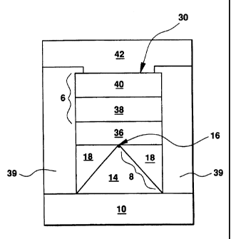
Referring to Fig. 1, shown is a cross-sectional view of a memory element
of the present invention formed on a single crystal silicon semiconductor
wafer 10.
The memory element includes the memory material 36, a first spacedly disposed
5 contact 6, and a second spacedly disposed contact 8. Both the first and
second
spacedly disposed contacts are used for supplying the electrical input signal
to the
memory material.
First contact 6 can be comprised of two thin-film layers. Thin-film layer 38,
deposited adjacent to the memory material 36 has excellent diffusion barrier
10 properties which inhibits the diffusion and electromigration of foreign
material into
the chalcogenide memory material 36.
The adjacent thin-film layer 38 may be comprised of a carbon material such
as amorphous carbon. Alternately, the adjacent thin-film layer 38 may be
formed
from a compound which includes one element selected from the group consisting
15 of Ti, V, Cr, Zr, Nb, M. Hf, Ta, W, and two or more elements selected from
the
group consisting of B, C, N, AI, Si, P, S. Preferably, the adjacent thin-film
layer 38
is formed from a compound which includes Ti and two or more elements selected
from the group consisting of C, N, AI, Si and mixtures or alloys thereof. In
one
embodiment, the adjacent thin-film layer is comprised of a compound having a
20 composition of, in atomic percent, between about 10% to 60% titanium, 5% to
50%
carbon and 10% to 60% nitrogen. In addition, the titanium carbonitride may
also
include up to 40% hydrogen.
In another embodiment, the adjacent thin-film layer 38 is comprised of
titanium siliconitride. Preferably, in this embodiment, the adjacent thin-film
layer
is comprised of a compound having a composition of, in atomic percent, between
about 10% to 60% titanium, 5% to 50% silicon and 10% to 60% nitrogen.
fn a third embodiment, the adjacent thin-film layer 38 is comprised of
titanium aluminum nitride. Preferably, in this embodiment, the adjacent thin-
film
layer is comprised of a compound having a composition of, in atomic percent,
between about 10% to 60% titanium, 5% to 50% aluminum and 10% to 60%
nitrogen.
The titanium carbonitride, titanium siliconitride and titanium aluminum
nitride
CA 02250504 1998-09-29
WO 97/40499 PCT/US97106538
21
have excellent barrier properties, preventing both the diffusion and
electromigration
of foreign material into the chalcogenide memory material. Furthermore, the
titanium carbonitride, titanium siliconitride and titanium aluminum nitride
may be
deposited by such methods as physical vapor deposition including evaporation,
ion
plating as well as DC and RF sputtering deposition, chemical vapor deposition,
and
plasma assisted chemical vapor deposition. The exact method used depends
upon many factors, one of which being deposition temperature constraints
imposed
by the composition of the chalcogenide target material.
The adjacent thin-film layer 38 is preferably deposited to a thickness of
about 100 ~ to 2000 ~. The adjacent thin-film layer 38 is more preferably
deposited to a thickness of about 200 ~ to 1000 ~.
First contact 6 can further comprise an additional thin-film layer 40
deposited
remote to the chalcogenide memory material. The remote thin-film layer is
comprised of one or more elements from the group consisting of Ti, W and Mo.
In one embodiment, the remote thin-film layer is comprised of Ti and W.
Preferably, the remote thin-film layer is comprised of a compound, in atomic
percent, of 5% to 30% titanium and 70% to 95% tungsten. The remote thin-film
layer Ti-W alloy is preferably deposited using a DC sputtering deposition
process.
It is preferably deposited to a thickness of about 100 A to 4000 A. It is more
preferably deposited to a thickness of about 200 A to 2000 ~,. The Ti-W alloy
has
excellent ohmic contact properties. Moreover, it has the barrier properties
necessary to prevent both the electromigration and diffusion of foreign
electrode
material into the chalcogenide memory material.
Figure 1 shows an embodiment of the second contact 8 which tapers in
cross-sectional area to a peak 16 that is adjacent to memory material 36. In
this
- embodiment, the second contact comprises a "contact tip" 14 that can be
formed
on the silicon substrate 10. The contact tip 14 can be formed in a multi-step
process. A patterned oxide layer can be formed on silicon substrate 10 using
conventional oxidation and photolithographic techniques. Using the oxide layer
as
a mask, the silicon substrate is anisotropically etched to form the elongated,
tapered structure on top of the silicon substrate 10 that is referred to as a
contact
tip. Contact tips can be fabricated so that they are conical, pyramidal,
elongated
CA 02250504 1998-09-29
WO 97/40499 PCT/US97/06538
22
or wedge-shaped. Other shapes that come to a point contact with the
chalcogenide material are also possible without departing from the spirit or
scope
of the instant invention.
The peak of the second contact can be pointed. Pointed peaks are
fabricated by sharpening the contact tips that are etched from the silicon
substrate.
Sharpening uses a reactive process which includes but is not limited to plasma
etching, wet chemical etching or thermal oxidation. Contact tips may also be
sharpened electrochemically, for example by placing a bias on a solution, and
depositing or etching the contact tips. This process may be used to sharpen
molybdenum, tungsten or precious metal contact tips such as platinum, pallium,
iridium or gold.
While it is preferred that the peaks are pointed, they need not be atomically
sharp. Peaks which are rounded or flat will also suffice provided the cross-
sectional diameter of each peak is sufficiently small. Preferably, the cross-
sectional diameter of the peak is less than 2000 ~. More preferably, the
diameter
of the cross-sectional area of the peak is less than 1000 ~. Most preferably,
the
diameter of the cross-sectional area of the peak is less than 500 ~. Contact
tips
which are formed having flat peaks can be fabricated as conical, pyramidal,
elongated or wedge-shaped frustums. In the most preferable embodiment, the
diameter of the peak will approximate the diameter of the filamentary pore
(the
conduction path) formed through the body of chalcogenide material.
Figure 2 shows another embodiment of second contact 8 in Which second
contact 8 includes a "first" thin-film layer 34. The first thin-film layer is
deposited
on top of contact tip 14. The first thin-film layer 34 may be comprised of a
carbon
material such as amorphous carbon.
- Alternately, the first thin-film layer 34 may be formed from a compound
which includes one element selected from the group consisting of Ti, V, Cr,
Zr, Nb,
M. Hf, Ta, W, and two or more elements selected from the group consisting of
B,
C, N, Al, Si, P, S. Preferably, the first thin-film layer 34 is formed from a
compound which includes Ti and two or more elements selected from the group
consisting of C, N, AI, Si and mixtures or alloys thereof.
In one embodiment, the first thin-film layer 34 is comprised of a compound
CA 02250504 1998-09-29
WO 97/40499 PCT/US97/06538
23
having a composition of, in atomic percent, between about 10 to 60% titanium,
5
to 50% carbon and 10 to 60% nitrogen. In addition, the titanium carbonitride
may
also include up to 40% hydrogen.
In another embodiment, the first thin-film layer 34 is comprised of titanium
siliconitride. Preferably, in this embodiment, the adjacent thin-film layer is
comprised of a compound having a composition of, in atomic percent, between
about 10 to 60% titanium, 5 to 50% silicon and 10 to 60% nitrogen.
In another embodiment, the first thin-film layer 34 may be comprised of
titanium aluminum nitride. Preferably, the first thin-film layer is comprised
of a
compound having a composition of, in atomic percent, between about 10 to 60%
titanium, 5 to 50% aluminum and 10 to 80% nitrogen.
The cross-sectional area of the peak of a second contact that includes a first
thin-film layer must be kept sufficiently small. As discussed above,
preferably, the
cross-sectional diameter of the peak is less than 2000 ~. More preferably, the
diameter of the cross-sectional area of the peak is less than 1000 ~. Most
preferably, the diameter of the cross-sectional area of the peak is less than
500
Alternately, the second contact 8 rnay comprise two thin-film layers, a first
and a second thin-film layer. The first thin-film layer is the same as
described
above. The second thin-film layer may be comprised of one or more elements
from the group consisting of Ti, W and Mo. In one embodiment, the second thin-
film layer is comprised of Ti and W. Preferably, the second thin-film layer is
comprised of a compound, in atomic percent, of 5% to 30% titanium and 70% to
95% tungsten. The two thin-film layers are arranged such that the second thin-
film
layer is deposited on top of the contact tip and the first thin-film layer is
deposited
on top of the second thin-film layer.
An alternate structure for the second contact 8 is one in which the contact
tip is offset from the silicon substrate by an elongated column. The elongated
column is used to increase the distance, and hence reduce the parasitic
capacitance, between the conducting electrodes that are used to supply current
to
the memory elements. Columns may be made of metal (for example sputtered
tungsten, single crystal metal such as tungsten or a sputtered titanium-
tungsten
CA 02250504 1998-09-29
WO 97/40499 PCT/US97/06538
24
alloy), conductive ceramic, silicon (doped or undoped), other semiconductor '
materials or other materials.
The spaces formed in the silicon substrate 10 by the etching process are
filled by depositing a suitable dielectric 18 on top of the second contact.
Examples
of suitable dielectric materials that may be used are TeOS, Si02 or SI3N4.
After
deposition of the dielectric material 18, the surtace is planarized using
chemical
mechanical polishing (CMP) techniques.
After CMP, a layer of chalcogenide memory material is then deposited on
top of the planarized surface. The layer of memory material 36 is formed of a
multi-element semiconductor material, such as the chalcogenide materials
disclosed herein. The layer 36 may be deposited by methods such as sputtering,
evaporation or by chemical vapor deposition (CVD), which may be enhanced by
plasma techniques such as RF glow discharge. The chalcogenide memory
materials of the instant invention are most preferably made by RF sputtering
and
evaporation. Typical deposition parameters for RF sputtering and evaporation
of
the chalcogenide layer 36 are set forth below in Tables 2 and 3, respectively.
Table 2
RF Sputtering Dep osition Parameters
Parameter Typical Range
Base pressure 8x10-' - 1x10- Torr
Sputtering gas 4 - 8 m Torr
_
(Ar) pressure
Sputtering power 40 - 60 Watts
Frequency 13 - 14 MHz
Deposition Rate 0.5 - 10 /second
Deposition Time 2 - 25 minutes
- Film Thickness 250 - 1500
Substrate Temp. Ambient - 300C
CA 02250504 1998-09-29
WO 97/40499 PCT/US97106538
Table 3
Evaporation Deposition Parameters
Parameter Typical Range
Base pressure 1x10-' - 5x10-' Torr
5 Evaporation Temp. 450 - 600 °C
Deposition Rate 2 - 4 /second
Deposition Time 2 - 20 minutes
Film Thickness 250 - 1500
Substrate Temp. Ambient - 300'C
It is important to note that evaporated films deposited on a heated substrate
exhibit anisotropic growth characteristics (see the description of Fig. 7) in
which
oriented layers of the chalcogenide elements are successively deposited.
Whether
this proves to be significant for electrical applications has yet to be
proven;
however, this type of film holds promise for thermoelectricity (due to the
high
thermopower already measured for these compositions, i.e., a factor of four
greater
than that measured for bismuth systems) or for specific semiconductor and
superconductivity applications. The layer of memory material 36 is preferably
deposited to a thickness of about 200 ~ to 5,000 ~, more preferably of about
250
~ to 2,500 l~ and most preferably of about 4D0 l~ to 1,250 l~ in thickness.
Deposited on top of the entire structure is a layer of insulating material 39.
Examples of insulating material that can be used are Si02, Si3N4 or TeOS. This
layer of insulating material is then etched and a layer of aluminum is
deposited to
form the second electrode grid structure 42 which extends perpendicular in
direction to the conductors 12 and complete the X-Y grid connection to the
individual memory elements. Overlaying the complete integrated structure is a
top
encapsulating layer of a suitable encapsulant such as Si3N4 or a plastic
material
such as polyamide, which seals the structure against moisture and other
external
elements which could cause deterioration and degradation of performance. The
Si3N4 encapsuiant can be deposited, for example, using a low temperature
plasma
deposition process. The polyamide material can be spin deposited and baked
after
deposition in accordance with known techniques to form the encapsulant layer.
The term "pore diameter" as used herein is the average cross-section of the
CA 02250504 1998-09-29
WO 97/40499 PCT/US97/06538
26
smallest region of contact between the memory material 3fi, and the electrical
contacts 6 and 8. The pore diameter can be as small as lithography resolution
limits will permit. Pore diameter is related to device performance. Reducing
pore
diameter reduces device volume. This increases the current density and energy
density of the device, thus lowering the current and energy requirements
needed
for electrical switching. This increases the speed and sensitivity of the
device -
reducing the switching time and electrical energy required to initiate the
detectable
change in resistance.
It is preferred that the pore diameter be selected to conform substantially
with the cross section of the memory material whose resistance is actually
altered
when the material is switched to either the high or low resistance state. This
section of memory material is called the "filamentary portion". Ideally, the
pore
diameter should equal the diameter of the filamentary portion.
As a means of reducing pore diameter beyond that permitted by lithography,
9 5 memory elements have employed "filament confining means" between at least
one
of the spacedly disposed contacts and the volume of memory material. The
filament confining means is, typically, a thin-film layer of highly resistive
material
with at least one low resistance pathway thereacross through which current
passes
between the electrical contact and the volume of memory material.
The filament confining means defines the size and position of the
filamentary portion within the memory material during both electrical
formation as
well as during switching of the memory element, thus providing a high current
density within the filamentary portion upon input of a very low electrical
current to
the spacedly disposed contacts.
The filament confining means plays a role in the "electrical formation
- - process" of the memory device. The electrical formation process consists
of
applying higher current electrical pulses to the newly constructed memory
element
until the memory element switches from its originally very high "virgin"
resistance
value to a lower resistance value. Once this occurs, the memory element is
said
to be "formed". It is now ready for subsequent lower current electrical
cycling.
The formation process "breaks down" the filament confining means. During
one or more of the higher current pulses applied during the formation process,
the
CA 02250504 1998-09-29
WO 97140499 PCT/US97/06538
27
electrically weakest "breakdown" region in the confining layer is physically
changed
and becomes much more highly conductive than the remainder of the layer. It is
through this region that all of the current of any subsequent memory cycling
pulses
(i.e. set and reset pulses) will pass. When a very low current is applied to
the
memory element, all of the current is channeled through the filamentary
portion.
Hence, because of its extremely small size, the current density is very high
within
this region of the memory material.
In the present invention, the second contact tapers in cross-sectional area
to a peak that is adjacent to the memory material. In general, the smaller the
area
within a cross-section of a volume, the higher the current density within that
cross
section. Hence, the small cross-sectional area at the peak creates a high
current
density at that location. A high current density is therefore applied to the
small
area of the memory material adjacent to the peak of the second contact.
The second contact thus serves a function similar to that of the filament
confining means described above. As with the filament confining means, the
second contact can define the size and position of the filamentary portion
within
the memory material during both electrical formation and during switching.
Hence,
the second contact of the present invention can be used to overcome the
lithography limitations creating a small pore without the need of using an
additional
layer of material.
The specially designed second contact of the present invention can also
lower the overall capacitance of the chalcogenide memory device. In
contradistinction to a memory device having two parallel contacts, the tapered
shape of the second contact increases the average distance between the two
memory contacts. This increase in average distance, decreases the average
electric field between the contacts which lowers both the capacitance and
energy
of the device.
The top view of a possible configuration for multiple memory elements is
shown in Fig. 3. As shown, the devices form an X-Y matrix of memory elements.
The horizontal strips 12 represent the X set of an X-Y electrode grid for
addressing
the individual elements. The vertical strips 42 represent the Y set of
addressing
lines.
CA 02250504 2005-06-08
28
It is important to note that conventional CMOS technology cannot be used to
produce this type of three dimensional memory array since CMOS technology
builds the
required semiconductor devices into the bulk of single crystal semiconductor
wafers and,
therefore, can only be used to fabricate a single layer of devices.
Furthermore, (1 ) CMOS
cannot produce as small of a footprint (actual element dimension) to
effectively produce
Large arrays at comparably low cost and (2) CMOS devices, because they exist
in a single
plane, cannot be interconnected along the Z direction. Therefore, CMOS devices
cannot
be fabricated with the complex, three-dimensional interconnectivity required
for advanced
parallel processing computers. The three-dimensional, thin-film memory array
structures
of the instant invention, on the other hand are capable of both conventional
serial
information processing as well as parallel information processing.
Parallel processing and therefore multidimensional memory array structures are
required for rapid performance of complex tasks such as pattern recognition,
classification
or associative learning etc. Further uses for and description of parallel
processing are
presented in U.S. Patent No. 5,159,661 which is assigned to the assignee of
the instant
application. With the integrated structure as shown in the embodiment of Fig.
1;
however, a completely vertically integrated memory structure can be formed,
thus
minimizing the area occupied on the substrate. This means that the density of
the memory
elements in the chip is limited essentially only by the resolution
capabilities of the
lithography.
Other circuit configurations for the electrically erasable memory of the
present
invention are, of course, possible and feasible to implement. One particularly
useful
configuration is a three dimensional, multilevel array in which a plurality of
planes of
memory or control elements and their respective isolation devices are stacked
upon one
another. Each plane of memory elements is arranged as a plurality of rows and
columns
of memory elements, thereby allowing for X-Y addressing. This stacking of
planes, in
addition to increasing memory storage density, allows for an additional Z
dimension of
interconnection. This arrangement is particularly useful to simulate a neural
network for
a truly intelligent computer.
CA 02250504 1998-09-29
WO 97/40499 PCT/US97/06538
29
Each memory element is electrically isolated from the others by using some
type of isolation element. Fig. 4, a schematic diagram of the memory device
layout, shows how electrical isolation can be accomplished using diodes. The
circuit comprises an X-Y grid with the memory elements 30 being electrically
interconnected in series with isolation diodes 26. Address lines 12 and 42 are
connected to external addressing circuitry in a manner well known to those
skilled
in the art. The purpose of the isolation elements is to enable each discrete
memory elements to be read and written without intertering with information
stored
in adjacent or remote memory elements of the matrix.
Fig. 5 shows a portion of a single crystal semiconductor substrate 50 with
a memory matrix 51 of the present invention formed thereon. Also formed on the
same substrate 50 is an addressing matrix 52 which is suitably connected by
integrated circuitry connections 53 to the memory matrix 51. The addressing
matrix 52 includes signal generating means which define and control the
setting
and reading pulses applied to the memory matrix 51. Of course, the addressing
matrix 52 may be integrated with and formed simultaneously with the solid
state
memory matrix 51.
In prior art semiconductor memories having the relatively high switching
speeds and low switching energies deemed necessary for most applications
thereof, at least one transistor and charge storage elements is required for
each
memory element. The formation of such memories in integrated circuit form
requires at least three connections along with other additional complexities
which
occupy a certain minimum substrate area regardless of how the integrated
circuit
is laid out. The integrated circuit configuration of the electrically erasable
memory
of the present invention requires only two connections to each memory element
- and these can be made in vertical relationship to each other. Further, each
memory element, complete with isolating diode and the pair of contacts for the
element, is itself fully vertically integrated such that a significantly
higher bit density
is possible. In fact, the memory of the present invention provides for a bit
density
which is greater than that attainable even in solid state dynamic random
access
memories (DRAMs), which are volatile and therefore lack the further advantages
that the non-volatility attainable with the present invention provides. The
increase
CA 02250504 1998-09-29
WO 97140499 PCT/US97/06538
in bit density attainable with the present invention translates into a
corresponding
reduction in manufacturing costs because of the smaller areas of the wafer
occupied per bit of the integrated circuit configuration. This allows the
memory of
the present invention to compete with and surpass other available memories for
5 a wider range of applications, not only in terms of electrical performance
and
memory storage capacity, but also in terms of cost. By comparison with prior
art
semiconductor memories formed of at least one transistor and a capacitor for
each
bit, the integrated circuit configurations of the present invention, as shown
in Fig.
1, can be formed on a chip with greater bit density compared to prior art
10 configurations using the same photo lithographic resolution. In addition to
the cost
advantages that the higher bit density affords, the elements are positioned
closer
together and lead lengths, capacitances, and other related parameters are
further
minimized, thereby enhancing pertormance.
Experimentation has shown that factors such as pore dimensions (diameter,
15 thickness and volume), chalcogenide composition, thermal preparation (post
deposition anneal), signal pulse duration, impurities such as oxygen present
in the
composition, crystallite size and signal pulse waveform shape have an effect
on
the magnitude of the dynamic range of resistances, the absolute end-point
resistances of said dynamic range, and the voltages required to set the device
at
20 these resistances. For example, relatively thick chalcogenide films (i.e.
about 4000
~) will result in higher set voltage requirements (and therefore higher
current
densities within the volume of memory material), while relatively thin
chalcogenide
layers (i.e. about 250 ~) will result in lower set voltage (and current
density)
requirements. Of course, the possible significance of crystallite size and,
therefore,
25 the ratio of the number of surface atoms relative to the number of bulk
atoms has
- previously been described.
The signal pulse duration required to set the memory element to the desired
resistance level within the dynamic range of electrical resistances will
likewise be
dependent upon all of the foregoing factors as well as signal current level.
30 Typically signal pulse durations will be less than about 250 nanoseconds
and
preferably less than about 50 nanoseconds. It is to be stressed that even the
short
25 nanosecond pulse widths noted are dependent on the size and shape of the
CA 02250504 1998-09-29
WO 97140499 PCT/I3S97/06538
31
pore as well as the thickness and composition of the semiconductor alloy
employed. It is believed that the pulse durations can be significantly reduced
without interfering with the operation of the memory switch. Experimentation
suggests that the input of lesser amounts of energy will increase the cycle
life of
the elements.
A feedback loop which reads and, when required, adjusts the resistance of
a given memory element may be incorporated into the memory systems of the
instant invention. For example, a memory element may initially be set at a
desired
resistance; however, in time the resistance of the element may drift slightly
from
the value at which it was originally set. The feedback loop, in this instance,
would
calculate and deliver a refresh signal pulse of the required voltage and
duration to
the memory element to bring it back to a preselected resistance value. Also,
circumstances may exist where the set pulse delivered to a memory element may
not result in setting of the element at the desired resistance value. In this
case the
feedback loop would deliver additional signal pulses to the element until the
desired resistance level is achieved. The total duration of this series of
setladjust
cycles is less than about 1,000 nanoseconds and preferably less than about 500
nanoseconds.
The ability ~ to reversibly move up and down the linear portion of the
resistance versus device current curve cannot be overemphasized. A pulse of a
selected current can set the memory element to a desired resistance,
regardless
of the previous set condition thereof. This ability to reversibly move along
the
curve provides for direct overwrite of previously stored data. Such direct
overwrite
capability is not possible with the phase change and MSM (a-Si) memory
materials
of the prior art. This ability to reversibly set intermediate resistance
values is
remarkable. A thousand successive medium current pulses achieves the same
resistance value as a higher current pulse followed by a single medium current
pulse or a lower current pulse followed by a single medium current pulse.
The dynamic range of resistances also allows for broad gray scale and
multilevel analog memory storage. Multilevel memory storage is accomplished by
dividing the broad dynamic range into a plurality of sub-ranges or levels. The
continuous resistance programmability allows for multiple bits of binary
information
CA 02250504 1998-09-29
WO 97!40499 PCT/US97/06538
32
to be stored in a single memory cell. This multilevel storage is accomplished
by
mimicking multiple bits of binary information in pseudo-analog form and
storing this
analog information in a single memory cell. Thus, by dividing the dynamic
range
of resistances into 2" analog levels, each memory cell would be provided with
the
capability of storing n bits of binary information.
As indicated hereinabove, Fig. 6 is a ternary diagram of the Ge-Te-Sb
semiconductor alloy system. In addition to the information previously
discussed
of which the binary and ternary phases are indicated by squares (~), this
diagram
gives information on the segregation of other alloys. These other alloys are
indicated by triangles (~), diamonds ( ~) and circles (~) and phases into
which the
alloys can segregate, upon rapid solidification from the melt, are indicated
by the
lines (solid or dashed) which extend therefrom. The starting compositions of
two
Te-rich melts are indicated by circular symbols on the ternary diagram. Upon
rapid
solidification, these mixtures phase segregate into elemental Te plus phases
B, C
and D.
Melts with compositions to the right of the pseudobinary line, indicated by
diamond symbols, solidify into the phases indicated by the lines on the
diagram.
Other mixtures, indicated by triangles in the phase diagram, solidify into
elemental
Ge and Sb and into phase A. An alloy of particular interest for use in the
improved
memory elements of the present invention is GeZ2SbZZTe56, also referred to as
Ge2SbzTeS or 2-2-5. This 2-2-5 alloy, upon rapid solidification, phase
segregates
into a mixture of two distinct phases of compositions B (GeZ6Sb,8Te56) and C
(Ge,8Sb26Tes6) indicated in the phase diagram of Fig. 6. Another alloy of
particular
interest is Ge,4Sb2sTe5, (also referred to as GeSbzTe4 or 1-2-4) which is
composition D on the GeTe-Sb2Te3 pseudobinary line. The 2-2-5 and 1-2-4 alloys
- are of interest for forming the volume of memory material in compositionally
graded, layered or combine gradedllayered form, as discussed hereinabove.
There is a threshold switching voltage associated with the programming of
the Ovonic EEPROM and, therefore, one expects that, like threshold switches,
the
Ovonic EEPROM programming voltage will show a chalcogenide alloy film
thickness dependence. In fact, in the Ovonic EEPROM, a threshold switching
voltage serves to separate read events from programming events, eliminating
read
CA 02250504 1998-09-29
WO 97140499 PCTlUS97/06538
33
upset and providing good operational margin during data reading. Our devices
show linear resistance characteristics when the applied field is low, followed
by a
gradual decrease in resistance with increasing field, up to a threshold
voltage.
Once the threshold voltage is exceeded, the device exhibits a negative
resistance
transition to a highly conductive, "dynamic on" state. When the applied field
is
removed, the device returns to a non-volatile programmed resistance state, the
value of which depends on the currentlenergy profile the device has
experienced
during its "memory equilibration time" while in the dynamic on state. Although
the
threshold voltage depends on the resistance of the device, the device current
at
the threshold voltage is relatively constant for all device resistances. A
linear
approximation to the thickness, threshold voltage relationship shows a
proportionality factor of less than one, which contributes to a wide operating
margin
in devices having the same nominal thickness.
Through the use of the proprietary materials and device configurations
disclosed herein, an electrically erasable, directly overwritable memory
element has
been developed which provides fast read and write speeds, approaching those of
SRAM devices; non-volatility and random access reprogramming capabilities of
an
EEPROM; and a price per megabyte of storage significantly below any other
semiconductor memory.
It is to be understood that the disclosure set forth herein is presented in
the
form of detailed embodiments described for the purpose of making a full and
complete disclosure of the present invention, and that such details are not to
be
interpreted as limiting the true scope of this invention as set forth and
defined in
the appended claims.