Note: Descriptions are shown in the official language in which they were submitted.
CA 022~6699 1998-11-26
W O 97/45827 PCTAUS96/07730
CrYstallization Processinq of Semiconductor Film Regions
on a Substrate and Devices Made Therewith
Technical Field
The invention relates to semiconductor
materials processing for semiconductor integrated
devices.
Background of the Invention
Semiconductor devices can be made in a layer or film
of silicon on a quartz or glass substrate, for example.
This technology is in use in the manufacture of image
sensors and active-matrix liquid-crystal display (AMLCD)
devices. In the latter, in a regular array of thin-film
transistors (TFT) on an appropriate transparent
substrate, each transistor serves as a pixel controller.
In commercially available AMLCD devices, the thin-film
transistors are formed in hydrogenated amorphous silicon
films (a-Si:H TFTs).
In the interest of enhanced switching
characteristics of TFTs, polycrystalline silicon has been
used instead of amorphous silicon. A polycrystalline
structure can be obtained by excimer-laser
crystallization (ELC) of a deposited amorphous or
microcrystalline silicon film, for example.
However, with randomly crystallized poly-
silicon, the results remain unsatisfactory. For small-
grained poly-silicon, device performance is hampered by
the large number of high-angle grain boundaries, e.g., in
the active-channel region of a TFT. Large-grained poly-
silicon is superior in this respect, but significant
grain-structure irregularities in one TFT as compared
with another then result in non-uniformity of device
characteristics in a TFT array.
. .. ~
CA 022~6699 1998-11-26
W O 97/4S827 PCTrUS96/07730
Summary of the Invention
For improved device characteristics and device
uniformity, a lateral solidification technique is applied
to a semiconductor film on a substrate. The technique,
which may be termed artificially controlled super-lateral
growth (ACSLG), involves irradiating a portion of the
film with a suitable radiation pulse, e.g. a laser beam
pulse, locally to melt the film completely through its
entire thickness. When the molten semiconductor material
solidifies, a crystalline structure grows from a
preselected portion of the film which did not undergo
complete melting.
In a preferred first embodiment of the
technique, an irradiated structure includes a substrate-
supported first semiconductor film, a heat-resistant film
on the first semiconductor film, and a second
semiconductor film on the heat-resistant film. In this
embodiment, both front and back sides of the structure
are irradiated with a pulse.
In a preferred second embodiment, lateral
solidification is from a first region via a constricted
second region to a third region which is intended as a
device region. One-sided irradiation is used in this
embodiment, in combination with area heating through the
substrate.
In a preferred third embodiment, a beam is
pulsed repeatedly in forming an extended single-crystal
region as a result of laterally stepping a radiation
pattern for repeated melting and solidification.
Advantageously, the technique can be used in
the manufacture of high-speed liquid crystal display
devices, wherein pixel controllers or/and driver
circuitry are made in single-crystal or regular/quasi-
regular polycrystalline films. Other applications
--2--
CA 022~6699 1998-11-26
W O 97145827 PCTIU~J'~7/~0
include image sensors, static random-access memories
(SRAM), silicon-on-insulator (SOI) devices, and three-
dimensional integrated circuit devices.
Brief DescriPtion of the Drawinqs
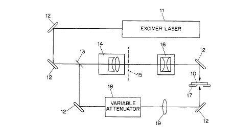
Fig. 1 is a schematic representation of a
projection irradiation system as can be used for the
first embodiment of the technique.
Fig. 2 is a schematic, greatly enlarged side
view of a sample structure for the first embodiment.
Figs. 3A and 3B are schematic, greatly enlarged
top views of TFT device microstructures which can be made
in semiconductor material of the first embodiment.
Fig. 4 is a schematic representation of an
irradiation system as can be used for the second
embodiment of the technique.
Fig. 5 is a schematic, greatly enlarged side
view of a sample structure for the second embodiment.
Figs. 6A-6D are schematic top views of the
sample structure of Fig. 5 at sequential stages of
processing.
Fig. 7 ia a schematic representation of an
irradiation system as can be used for the third
embodiment.
Fig. 8 is a schematic, greatly enlarged side
view of a sample structure for the third embodiment.
Figs. 9A-9F are schematic top views of a sample
structure with side view as in Fig. 8 at sequential
stages in a first version of a first variant of
processing.
Figs. lOA-lOF are schematic top views of a
sample structure with side view as in Fig. 8 at
sequential stages in a second version of the first
variant of processing.
CA 022~6699 1998-11-26
W 097/45827 PCTrUS96/07730
Figs. llA-llC are schematic top views of a
sample structure at sequential stages of a second variant
of processing.
Fig. 12 is a schematic top view of a liquid-
crystal display device in which TFTs are included.
Detailed Description of Preferred Embodiments
Described in the following are specific,
experimentally realized examples, as well as certain
variations thereof. Explicitly or implicitly, some
variations are common to more than one of the
embodiments, and further variations, within the scope of
the claims, will be apparent to those skilled in the art.
Included, e.g., is the use of semiconductor materials
other than silicon, such as germanium, silicon-germanium,
gallium arsenide or indium phosphide, for example.
Included also is the use of a substrate of any suitable
material, e.g., silicon, quartz, glass or plastic,
subject to considerations of stability, inertness and
heat resistance under processing conditions. And
included is the use of a radiation beam other than a
laser beam, e.g., an electron or ion beam.
First Embodiment
The projection irradiation system of Fig. 1
includes an excimer laser 11, mirrors 12, a beam
splitter 13, a variable-focus field lens 14, a patterned
projection mask 15, a two-element imaging lens 16, a
sample stage 17, a variable attenuator 18 and a focusing
lens 19. With this system, simultaneous radiation pulses
can be applied to the front and back sides of a sample 10
on the stage 17.
For the first embodiment of the technique, a
"dual-layer" (DL) sample structure was prepared as shown
CA 022~6699 1998-11-26
W O 97/45827 PCTrUS96/07730
in Fig. 2, including a transparent substrate 20, a first
amorphous silicon film 21, an SiO2 film 22, and a second
amorphous silicon film 23. Film thicknesses were
100 nanometers for the amorphous silicon films and
500 nanometers for the SiO2 film. Alternative heat-
resistant materials such as, e.g., silicon nitride or a
high-temperature glass may be used for the film 22.
With pattern projection onto the second or top
silicon film 23 and broad-beam irradiation of the first
or bottom silicon film 21, the first silicon film 21 can
be regarded as a sacrificial layer which is included
favorably to affect the thermal environment for maximized
lateral crystal growth in the top silicon film 23. The
roles of these films is reversed if, alternatively, the
pattern is projected through the substrate onto the first
film. In the pattern-irradiated film, large, laterally
solidified grains will be formed, making the processed
film well-suited for TFTs, for example.
Structures in accordance with Fig. 2 were
prepared by sequential low-pressure chemical vapor
deposition (LPCVD) of a-Si, sio2, and again a-Si on a
quartz substrate. Other suitable deposition methods, for
producing amorphous or microcrystalline deposits, include
plasma-enhanced chemical vapor deposition (PECVD),
evaporation or sputtering, for example.
Samples were placed onto the stage 17 of the
projection irradiation system of Fig. 1. The mask 15 had
a pattern of simple stripes 50 micrometers wide, with
various separation distances from 10 to 100 micrometers.
The mask pattern was projected onto the samples
with different reduction factors in the range from 3
to 6. The back-side energy density was controlled by the
variable attenuator 18. Samples were irradiated at room
temperature with a 30-nanosecond XeC1 excimer laser pulse
--5--
CA 022~6699 1998-11-26
W O 97/45827 PCTrUS96/07730
having a wavelength of 308 nanometers, quartz being
transparent at this wavelength. Such a laser is
commercially available under the designation LambdaPhysik
Compex 301. For a glass substrate, a longer wavelength
would have been required, e.g., 348 nanometers.
Irradiation was with fixed front-side energy
density and with various back-side energy densities.
Estimated front-side energy density was approximately
1.0 J/cm2 at the sample plane. The back-side energy
densities were in the range from 170 to 680 mJ/cm2.
For examination subsequent to irradiation, the
films were thoroughly defect-etched using Secco etchant
and examined using scanning electron microscopy (SEM).
The largest, most uniform grains were obtained at a back-
side energy density of 510 mJ/cm2. These grains grewlaterally from the two sides of stripe regions, forming
two rows of grains with a well-defined grain boundary at
the center line of the stripe.
Even if the resulting individual crystals may
not be large enough to accommodate the entire active-
channel region of a TFT, they form a regular or quasi-
regular polycrystalline structure which can serve as
active-channel region of a TFT, e.g., as illustrated in
Fig. 3A or Fig. 3B. Shown are a source electrode 31, a
drain electrode 32, a gate electrode 33 and an active-
channel region 34. In Fig. 3A, the active-channel region
includes both rows of grains produced as described above.
With grains sufficiently large as in Fig. 3B, the active-
channel region can be formed by a single row of grains.
In processing according to the first
embodiment, the role of the sacrificial bottom film 21
may be understood as being that of a heat susceptor which
stores energy when heated by the beam, the greatest
benefit being obtained when this film melts. The stored
CA 022~6699 1998-11-26
W O 97/45827 PCTAUS9C~
heat is released during solidification. This decreases
the degree to which the top film 23 loses heat by
conduction. Accordingly, for maximum benefit, care is
called for in proper dimensioning of the irradiated
structure. If the sio2 film 22 is too thin, the thermal
evolution of the silicon films 21 and 23 will tend to
track together, without significant benefit from the
inclusion of the film 21. On the other hand, if the
film 22 is too thick with respect to the thermal
diffusion length of the physical process, the film 21
will have insufficient influence on the transformation in
the top film 23. As to the bottom film 21, its thickness
should be chosen for this film to have sufficient thermal
mass. But the thicker the film 21, the more energy will
be required for its melting.
As alternatives to projection of a pattern onto
the silicon layer 23, a desired pattern may be defined
there by a proximity mask, a contact mask, or a deposited
mask layer which is patterned photo-lithographically, for
example.
In one variant of masking, a mask layer may
serve to reduce heating in the area beneath the mask,
e.g., by absorbing or reflecting incident radiation.
Alternatively, with a suitable mask material of suitable
thickness, a complementary, anti-reflection effect can be
realized to couple additional energy into the
semiconductor film beneath the mask material. For
example, an SiO2 film can be used to this effect on a
silicon film. This variant is advantageous further in
that the mask layer can serve as a restraint on the
molten semiconductor material, thus preventing the molten
semiconductor layer from agglomerating or deforming under
surface tension.
CA 022~6699 1998-11-26
W O 97/458~7 PCT/U~3~ 7/~0
Second Embodiment
The irradiation system of Fig. 4 includes an
excimer laser 41, a prism deflector 42, a focusing
lens 43, a vacuum chamber 44 and a hot stage 45 on which
a sample 40 is disposed.
For the second embodiment of the technique and
using the irradiation system of Fig. 4, the sample
structure of Fig. 5 includes a substrate 50, a thermal
oxide film 51, a first patterned amorphous silicon
film 52, an sio2 film 53, a second patterned silicon
film 54, and a further deposited sio2 film 55. Typical
thicknesses are 100 nanometers for the thermal oxide
film 51, 100 nanometers for the a-Si film 52, 210
nanometers for the SiO2 film 53, 120 nanometers for the
a-Si film 54, and 170 nanometers for the sio2 film 55.
Such a sample structure was prepared by
depositing the amorphous silicon film 52 by low-pressure
chemical vapor deposition (LPCVD) onto the thermal oxide
film 51 on a silicon wafer 50. The silicon film 52 was
coated with a photoresist which was then exposed in a
stepper and developed, and the silicon film 52 was
reactively ion-etched in SF6/02 plasma for patterning.
The resulting pattern of a "first-level island" of the
silicon film 52 is shown in Fig. 6A as viewed from the
top. The pattern consists of three parts: a square
"main-island" region 523 which is intended for eventual
device use, a rectangular "tail" region 521, and a narrow
"bottleneck" region 522 connecting the tail region 521
with the main-island region 523. Dimensions were chosen
as follows: 20 by 10 micrometers for the tail
region 521, 5 by 3 micrometers for the bottleneck
region 522, and different dimensions in the range from 10
by 10 to 50 by 50 micrometers for the main-island
region 521.
--8--
. _
CA 022~6699 1998-11-26
W O 97/45827 PCTAJS96/07730
The first-level islands were encapsulated with
the SiO2 film 53 by plasma-enhanced chemical-vapor
deposition (PECVD), and amorphous silicon was deposited
on top. Photolithographic processing was used again, for
patterning the amorphous silicon film as a "second-level
island" 54 dimensioned 5 by 5 micrometers. The second-
level island 54 is positioned directly above the tail
region 521 to serve as a beam blocker during irradiation.
Last, the entire structure was encapsulated with PECVD
10 Sio2.
For processing, a sample was placed on a
resistively heated graphite hot stage inside a vacuum
chamber at a pressure of 10-5 torr. Vacuum-processing can
be dispensed with if a suitable alternative heater is
available. Heating was to a substrate temperature
of 1000 to 1200 ~C, which required a ramp-up time
interval of about three minutes. Before irradiation, the
sample was held at the final substrate temperature for
approximately two minutes. The sample temperature was
monitored occasionally by a directly attached
thermocouple and continuously by a digital infrared
thermometer. The sample was irradiated with a single
excimer-laser pulse at energy densities that were
sufficiently high to completely melt all of the first-
level island except for the beam-blocked area within the
tail region.
For analysis of the microstructure, the
irradiated samples were Secco-etched. For samples
irradiated at a substrate temperature of 1150 ~C, optical
Nomarski micrographs of the Secco-etched samples showed
complete conversion of islands 20 by 20, 40 by 40 and 50
by 50 micrometers into single-crystal islands (SCI).
Defect patterns in the etched samples suggest that the
main-island zones contain low-angle sub-boundaries
CA 022~6699 1998-11-26
W O 97/45827 PCTrUS96/07730
similar to those observed in zone melting
recrystallization (ZMR), as well as planar defects which
have been identified in SLG studies. At a lower
substrate temperature, such as at 1100 ~C, only the
smaller, 20-by-20 micrometer islands were converted into
single-crystal islands free of high-angle grain
boundaries. And at still-lower substrate temperatures
of 1050 ~C and 1000 ~C, high-angle grain boundaries
appeared even in the 20 by 20 micrometer islands.
The solidification sequence in this second
embodiment may be understood with reference to Figs. 6B-
6D as follows: Upon irradiation, the second-level
square 54 blocks most of the beam energy incident on the
area, which prevents complete melting in the beam-blocked
area of the tail region 521. The rest of the exposed
first level regions melts completely as illustrated by
Fig. 6B. As the film is conductively cooled through the
substrate, the liquid-solid interface at the beam-blocked
region undercools, and silicon grains 61 start to grow
radially outward from the beam-blocked region. Within
the tail region 521 , many of the grains 61 are quickly
occluded, and only one or a few favorably located grains
grow toward the bottleneck 522. The bottleneck 522 is
configured such that just one of these grains expands
through the bottleneck 522 into the main-island
region 523. ~f the substrate temperature is high enough
and the main island 523 is small enough to prevent
nucleation in the super-cooled liquid, lateral growth of
the one grain that grew through the bottleneck 522
converts the entire main island 523 into a single-crystal
region.
Thus, successful conversion of the main-island
region 523 into single-crystal form requires a suitable
combination of substrate temperature and island size.
--10--
CA 022~6699 1998-11-26
W O 97/45827 PCTrUS96/07730
The molten silicon must be sustained at a temperature
which is sufficiently high for the characteristic time of
nucleation for a specific volume to be much longer than
the characteristic time required for the complete
conversion by lateral solidification. Since the
characteristic conversion time depends mainly on the
distance to be converted, i.e., the lateral dimension of
the main island, the island size must be related to the
substrate temperature such that the characteristic
conversion time is commensurate with the average lateral
growth distance that can be achieved before any
nucleation is triggered within the liquid. As compared
with zone-melting recrystallization, the present
technique allows the recrystallization of very thin
films, e.g., having a thickness of 100 nanometers or
less.
Instead of by beam blocking, a seed region can
be defined by complementary masking with an anti-
reflection film, as described above for the first
embodiment. Alternatively further, a seed region can be
defined by projection.
Third Embodiment
The projection irradiation system of Fig. 7
includes an excimer laser 71, mirrors 72, a variable-
focus field lens 74, a patterned mask 75, a two-element
imaging lens 76, a sample stage 77, and a variable
attenuator 78. A sample 70 is disposed on the sample
stage 77. This system can be used to produce a shaped
beam for stepped growth of a single-crystal silicon
region in a sequential lateral solidification (SLS)
process. Alternatively, a proximity mask or even a
contact mask may be used for beam shaping.
CA 022~6699 1998-11-26
W 097/45827 PCTrUS96/07730
The sample structure of Fig. 8 has a
substrate 80, a thermal oxide film 81, and an amorphous
silicon film 82.
In the following, the third embodiment of the
technique is described with reference to Figs. 9A-9F and
lOA-lOF showing two versions of a first variant, and
Figs. llA-llB showing a second variant.
Starting with the amorphous silicon film 82,
which in this exemplary embodiment is patterned as a
rectangle (Fig. 9A), a region 91, bounded by two broken
lines, of the silicon film 82 is irradiated with a
pulse, to completely melt the silicon in that region
(Fig. 9B), and then resolidify the molten silicon (Fig.
sC) in the region 91. Here, the region 91 is in the
shape of a stripe, and irradiation of the region 91 may
be by masked projection or by use of a proximity mask.
Upon resolidification of the molten silicon in the region
91, two rows of grains grow explosively from the broken
line boundaries of the region 91 towards the center of
the region 91. Growth of the two rows of grains is over
the characteristic lateral growth to a final distance 92.
In any remainder of region 91, a fine grained
polycrystalline region 93 is formed. Preferably, the
width of the stripe is chosen such that, upon
resolidification, the two rows of grains approach each
other without converging. Greater width, which is not
precluded, does not contribute to the efficacy of
processing. Lesser width tends to be undesirable since
the subsequent step may have to be reduced in length, and
the semiconductor surface may become irregular where
grains growing from opposite directions come together
during the solidification process. An oxide cap may be
formed over the silicon film to retard agglomeration and
constrain the surface of the silicon film to be smooth.
-12-
CA 022~6699 1998-11-26
W O 97/45827 PCT~US96/07730
A next region to be irradiated is defined by
shifting (stepping) the sample with respect to the masked
projection or proximity mask in the direction of crystal
growth. The shifted (stepped) region 94 is bounded by
two broken lines in Fig. 9D. The distance of the shift
is such that the next region to be irradiated 92 overlaps
the previously irradiated region 91 so as to completely
melt one row of crystals while partially melting the
other row of crystals, as shown in Fig. 9E. Upon
resolidification, the partially melted row of crystals
will become longer, as shown in Fig. 9F. In this
fashion, by repeatedly shifting the irradiated portion,
single crystalline grains of any desired length may be
grown.
If the pattern of the irradiated region is not
a simple stripe, but is in the shape of a chevron 101, as
defined by the broken lines in Fig. lOA, the same
sequence of shifting the irradiated region shown in Figs.
lOB-lOF will result in the enlargement of one grain
growing from the apex of the trailing edge of the
shifting (stepping) chevron pattern. In this manner, a
single-crystal region can be grown with increasing width
and length.
A large area single-crystal region can also be
grown by applying sequentially shifted (stepped)
irradiation regions to a patterned amorphous silicon
film, such as that illustrated in Fig. llA, having a tail
region 111, a narrow bottleneck region 112 and a main
island region 113. The cross-section of regions 111, 112
and 113 in Figs. llA-llC is similar to that shown in Fig.
5, except that the radiation blocking amorphous silicon
- region 54 and the second silicon dioxide layer 55 are
absent. The region of irradiation defined by masked
projection or a proximity mask is illustrated by the
-13-
CA 022~6699 1998-11-26
W O 9714S827 PCTAUS96tO7730
regions bounded by broken lines in Figs. llA-llC, which
also show the sequential lateral shifting (stepping) of
the irradiated region to obtain the growth of a single
grain from the tail region 111 through the bottleneck
region 112 to produce a single crystal island region 113.
Sequential lateral melting and resolidification
in the examples of Figs. 9A-9F, 10A-lOF and llA-llC were
carried out on amorphous silicon films which had been
deposited by chemical vapor deposition (CVD) on a silicon
dioxide coated quartz substrate, with film thicknesses
from 100 to 240 nanometers. The production of single-
crystal stripes was confirmed in optical and scanning
electron microscopic examination of defect-etched
samples.
Optionally, the substrate may be heated, e.g.,
to reduce the beam energy required for melting or to
lengthen the lateral growth distance per step. Such
benefits may be realized also by two-sided irradiation of
a sample on a stage as shown in Fig. 1.
Further Processinq and A~plications
With a semiconductor film processed by the
present technique, integrated semiconductor devices can
be manufactured by well-established further techniques
such as pattern definition, etching, dopant implantation,
deposition of insulating layers, contact formation, and
interconnection with patterned metal layers, for example.
In preferred thin-film semiconductor transistors, at
least the active-channel region has a single-crystal,
regular or at least quasi-regular microstructure, e.g.,
as illustrated by Figs. 3A and 3B.
of particular interest is the inclusion of such
TFTs in liquid-crystal display devices as schematically
shown in Fig. 12. Such a device includes a substrate 120
-14-
CA 022~6699 1998-11-26
W O 97145827 PCTrUS96/07730
of which at least a display window portion 121 is
transparent. The display window portion 121 includes a
regular array of pixels 122, each including a TFT pixel
controller. Each pixel controller can be individually
addressed by drivers 123. Preferably, pixel controllers
or/and driver circuitry are implemented in semiconductor
material processed in accordance with the technique of
the present invention.
Other applications include image sensors,
static random-access memories (SRAM), silicon-on-
insulator (SOI) devices, and three-dimensional integrated
circuit devices.