Note: Descriptions are shown in the official language in which they were submitted.
CA 02307816 2000-04-27
WO 99/22302 PCT/US98/22807
-1-
BUFFERING DATA THAT FLOWS BETWEEN BUSES OPERATING
AT DIFFERENT FREQUENCIES
TECHNICAL FIELD
The invention relates to data buffering, and more particularly to buffering
data that flows between buses operating at different frequencies.
BACKGROUND INFORMATION
A typical computer system includes multiple data buses that facilitate the
flow of data between various components of the system. In general, the data
buses are
of different types that operate according to different functional standards,
such as the
Industry-Standard Architecture (ISA), Extended Industry-Standard Architecture
(EISA), Peripheral Component Interface (PCI), and Small Computer System
Interface
(SCSI) standards. Among the characteristics that distinguish the different
types of
data buses is operating frequency, or the rate at which a bus transfers data
among
components residing on the bus. In a typical computer system, data routinely
is
1 S transferred between devices located on different buses operating at
different
frequencies. For example, a microprocessor located on a host bus operating at
SO
MHz often must deliver data to a device located on a PCI bus operating at 8
MHz. To
compensate for such disparities in operating frequency, the computer system
must
include a buffering system between the data buses.
Conventional buffering systems employ standard memory devices as first-
in, first-out (FIFO) buffers. A typical FIFO buffer usually has two ports, one
of which
receives data from a first bus at a first data rate while the other delivers
the data to a
second bus at a second data rate. FIFO buffering schemes require careful
synchronization of read and write controllers to prevent data from overflowing
or
underflowing the FIFO buffers. Some FIFO buffering schemes use multiple memory
devices to create multiple FIFO buffers; such as in the well-known "double-
buffering" techniques, where one of a pair of separately addressable buffers
has data
written to it while the other buffer is being read. The roles of the separate
buffers are
periodically switched.
CA 02307816 2000-04-27
WO 99/Z2302 PCT/US98/22807
-2-
Various techniques have been used to work around the buffer synchronism
problem. One technique is to have the write side and the read side of a single
buffer
operate in a mutually exclusive fashion. Write control logic puts data into
the buffer
until the buffer is full, and then signals read control logic to start reading
the content.
When the reading is completed, the read control logic signals the write
control logic
to start filling the buffer again. This process continues until all data is
transferred.
This is a fool-proof method to guarantee the data integrity, but the drawback
is long
latency since at least one side of the buffer is idle at any given time.
Another method of determining FIFO full/empty status is by comparing
the read and the write pointers of a FIFO. If the two pointers line up and the
last
operation is a write command, the FIFO is full. If the last operation is a
read
command when the two pointers lines up, the FIFO is empty. This method works
well
when the read and write control logic are both running at the same clock
speed. When
the two sides are running at two different clock speeds, there is a potential
to produce
an erroneous or inconclusive empty/full status, and thus there may be a danger
of data
corruption.
Accordingly, the inventors have concluded that a better approach is need
to buffering data that flows between buses operating at different frequencies.
The
present invention provides a system and method for achieving this objective.
SUMMARY
The invention features a "virtual FIFO" system for use in buffering data
between transacting buses that transfer data at different rates. The system
includes a
memory device partitioned into multiple banks, each of which is configured to
operate
as a distinct data buffer. Such partitioning may be done on a dynamic, "on-the-
fly"
basis. The invention eliminates the possibility of FIFO status ambiguity while
maintaining FIFO efficiency by allowing both read and write operations to
operate
concurrently.
CA 02307816 2000-04-27
wo 99nZ3oz Pcrius9snZSO7
-3-
In the preferred embodiment, the memory device is a two-port (one read,
one write) random access (R.AM) device configured as a FIFO. A two-port RAM
allows independent and random access to any location of the RAM from both the
read
and the write side of the FIFO. A write controller generates a write strobe to
the RAM
and controls write address generation. A read controller is responsible for
controlling
read address generation.
While the RAM FIFO allows read and write access concurrently, for any
particular bank, only one of the two operations is allowed, such that the read
controller and the write controller never access the same logical bank at the
same
time. This prevents all overflow and underflow conditions.
In one embodiment, the system includes status flags associated with each
data buffer, one flag indicating whether data may be written to the data
buffer, and
another flag indicating whether data may be read from the data buffer. The
status
flags may be stored in the memory device itself or in another memory
structure. In an
alternative embodiment, a single binary status flag is used to indicate the
read/write
state of the data buffer.
In another embodiment, the controller that partitions the memory device
into multiple data buffer banks also manages data flowing into and out of the
data
buffers. The controller may include separate write and read controllers, which
may
use the status flags discussed above to determine when to write data to and
read data
from the data buffers.
Advantages of the invention include one or more of the following:
Using a single memory device to create multiple data buffers yields
an efficient and effective data buffering system that is less
expensive than previous systems.
Data from one or more data transactions may be written to and read
from the buffering system in an interleaved, concurrent fashion.
CA 02307816 2000-04-27
WO 99/22302 PCT/US98/22807
-4-
A single memory device may be used to buffer data between two
buses operating at different frequencies without underflowing or
overflowing, regardless of a substantial disparity in the buses'
operating frequencies.
The details of one or more embodiments of the invention are set forth in
the accompanying drawings and the description below. Other features, objects,
and
advantages of the invention will be apparent from the description and
drawings, and
from the claims.
DESCRIPTION OF DRAWINGS
FIG. 1 is a block diagram of various components in a computer system.
FIG. 2 is a block diagram of a system for buffering data that flows
between data buses operating at different frequencies.
FIG. 3 is a timing diagram for one embodiment of the invention.
Like reference numbers and designations in the various drawings indicate like
elements.
DETAILED DESCRIPTION
Refernng to FIG. 1, a computer system 10 includes at least two data buses
that facilitate data transfers among components of the computer system. One of
these
data buses, the primary bus 12, is a "host" bus dedicated to carrying out data
transactions involving the computer's central processing unit (CPU) 14 and
main
memory 16. The host bus 12 operates at a first frequency (e.g., 50 MHz). A
secondary
bus 18 carnes out transactions involving other devices 20, 22 in the computer
system
10, including transactions between the devices 20, 22 themselves, as well as
transactions between one or more of the devices 20, 22 and the CPU 14. The
secondary bus, which may be any type of data bus (e.g., ISA, EISA, PCI, SCSI),
operates at a second frequency (e.g., 8 MHz). The devices 20, 22 residing on
the
CA 02307816 2000-04-27
WO 99/22302 PCT/US98/22807
-5-
secondary bus 18 may be any types of devices, including peripheral devices
such as a
video card or a network interface card (NIC), and input/output (UO) devices
such as a
keyboard or a printer.
The primary bus 12 and the secondary bus 18 are connected by a bridge
S device 24 which manages data transactions between the two buses. The bridge
device
24 may serve both as a translator to interpret commands originating on one bus
for
delivery to the other bus and as a buffering system for data transfers
associated with
the commands. The buffering scheme employed by the bridge device 24 is
described
below. A primary bus controller 26 manages competing requests from the CPU 14
and the bridge device 24 for access to the primary bus 12, in known fashion.
Likewise, a secondary bus controller 28 manages competing requests from
the secondary devices 20, 22 and the bridge device 24 for access to the
secondary bus
18.
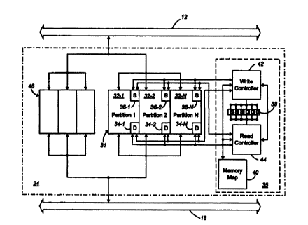
Referring to FIG. 2, the bridge device 24 employs a "virtual FIFO"
buffering scheme in which a single FIFO memory device 31 is partitioned into N
distinct memory regions ("banks") 32-1, 32-2, ... 32-N by a controller 35.
Preferably,
each bank comprises a continuous block of memory addresses. The controller 35
treats the banks 32-1, 32-2, ... 32-N as distinct FIFO buffers, each of which
may store
data independently of or in conjunction with the other banks. For example, the
banks
32-1, 32-2, ... 32-N may be used individually to buffer data associated with
multiple
distinct transactions, or they may be used together to buffer data associated
with
fewer but larger transactions. A bank may range in size from one word (e.g.,
two
bytes) of data to the entire storage capacity of the memory device 31.
Therefore, the
memory device 31 may contain as few as one bank, or it may contain as many
banks
as data words that it can store. The trade off is the number of status flags
that the read
and write controllers need to track, the complexity of the controller, and the
efficiency
of the FIFO. That is, as N grows bigger, the FIFO efficiency increases, but
the
number of status flags and the complexity of the controller also increases. In
the
illustrated embodiment, a memory map 40 created and maintained by the
controller
CA 02307816 2000-04-27
WO 99/22302 PCT/US98/22807
-6-
35 identifies the memory addresses that define the boundaries of the banks 32-
1, 32-2,
. . . 32-N, regardless of how many banks have been created.
A write controller 42 manages the flow of data into the banks 32-1, 32-2,
. . . 32-N, and a read controller 44 manages the flow of data out of the
banks. The
write and read controllers 42, 44 may be implemented, for example, as state
machines. The write and read controllers 42, 44 allow data to be written to
one bank
and read from another bank in the memory device 31 concurrently. The
controllers
42, 44 ensure the integrity of data in the buffers by allowing a device to
begin writing
data into a bank only when the bank is empty, and to begin reading from a bank
only
when the bank is full.
Each bank 32-l, 32-2, ... 32-N has at least two associated status flags: a
"done" flag 34-1, 34-2, ... 34-N that indicates to the write controller 42
that the
corresponding bank 32-1, 32-2, ... 32-N is empty and can accept data from a
writing
device; and a "start" flag 36-1, 36-2, ... 36-N that indicates to the read
controller 44
1 S that the corresponding bank is full and therefore can provide data to a
reading device.
The write controller 42 clears the "done" flag for a bank when a writing
device begins
placing data into the bank. The write controller 42 then sets the bank's
"start" flag
when the bank is full or, alternatively, when the writing device concludes its
data
transfer before the bank is full. Likewise, the read controller 44 clears the
"start" flag
for a bank when a reading device begins taking data from the bank and then
sets the
"done" flag when the bank is empty. In a preferred embodiment, the "start" and
"done" flags are both cleared at the beginning of a data transfer and at
"power on".
For maximum data integrity, the "start" flag of a bank is also used to clear
the "done"
flag of that same bank, and the "done" flag is used to clear the "start" flag
of the bank.
Such an interlock hand-shake mechanism allows the clock rates from both side
of the
FIFO to be completely independent of each other and there is no limit on the
operation range.
The "start" and "done" flags may be stored in any of several locations,
including the following: within the banks 32-1, 32-2, ... 32-N, within the
memory
device 31 but outside of the banks 32-l, 32-2, ... 32-N, or in another memory
CA 02307816 2000-04-27
WO 99/22302 PCT/US98/22807
structure 38, such as a register (register 38 will not be present if the
"start" and
"done" flags are stored in the memory device 31 ). Alternatively, the write
and read
controllers 42, 44 may keep internal "start" and "done" flags, and each
controller 42,
44 may send a message directly to the other controller 44, 42 upon filling or
emptying
S a buffer.
In an alternative embodiment, a single binary status flag is used to indicate
"start" and "done." In this case, the write controller 42 cannot write to a
bank until the
flag for the bank is set to "done." The write controller 42 then writes to
that bank,
and, when done writing, resets the corresponding flag to "start." Similarly,
the read
controller 44 cannot read from a bank until the corresponding flag is reset to
"start."
After reading all of a bank, the read controller 44 sets the corresponding
flag to
"done." However, in this embodiment, care should be taken to prevent a "race"
condition, where one controller is reading the state of a flag and acting on
it while the
other controller is changing the flag.
To ensure that the "virtual FIFO" buffering scheme functions properly
regardless of the data transfer rates of the data buses 12, 14, the write
controller 42
synchronizes its setting of the "start" flags to the read controller's
internal clock (not
shown), and the read controller 44 synchronizes its setting of the "done"
flags to the
write controller's internal clock (not shown). The "start" and "done" flags
provide a
mechanism that ensures that the read and write controllers 42, 44 never access
the
same logical bank at the same time. This prevents all overflow and underflow
conditions. The "virtual FIFO" buffering scheme provides sufficient buffering
despite
wide differences in the operating frequencies of the data buses.
In addition to at least one memory device 31 having multiple data buffer
banks, the bridge device 24 may include one or more additional memory devices
46,
each of which also may be partitioned as described above. In this situation,
memory
controller 35 may be used to manage all memory devices in the bridge device
24, or a
separate memory controller may be provided for each memory device in the
bridge.
Each of the memory devices 3 l, 46 may be embodied in a single random access
memory (RAM) integrated circuit. Alternatively, such memory devices 31, 46 may
be
CA 02307816 2000-04-27
WO 99/22302 PCT/US98/22807
-g_
embodied in a memory module (e.g., a SIMM or DIMM) comprising such integrated
circuits and functioning as a single addressable device. In either case, the
memory
devices 31, 46 may include volatile or non-volatile memory, and may be of any
RAM
type (e.g., DRAM, SRAM, EDO-RAM, etc.), but is preferably static RAM. The
memory devices 31, 46 may be partitioned into banks of equal size, or the
banks may
be of different sizes, which may be useful, e.g., in applications using
asymmetric data
transfers. Each memory device may be permanently partitioned once, or the
banks
may be defined dynamically as needed. The "start" and "done" flags described
above
typically will be a single bit in length, but flags of other sizes (e.g.,
nibbles, bytes,
words, etc.) also may be used. Alternatively, as noted above, a single bit may
be used
for each "start" and "done" flag pair (i.e., toggling between high and low
logic levels
may be used to indicate the "start" and "done" conditions).
Optionally, each bank may have an associated "last" flag, which indicates
that a bank is the last bank for a current data transfer operation. In such a
configuration, data is written into the FIFO in the sequential fashion (i.e.,
bank 32-1 is
written until full, then bank 32-2, ..., 32-N, and back to bank 32-1. Data is
read out in
a similar sequential fashion.
After a bank is filled, the write controller 42 sets the corresponding "start"
flag for the bank. As the last location of a bank is written, the write
controller 42
checks the "start" flag of the next bank. If that "start" flag is cleared (the
bank is
empty), the write controller 42 will continue the write operation. If the
"start" flag of
the next bank is not cleared (the bank is not empty), the write operation will
pause.
However, the write controller 42 continues to monitor the "start" flag of
the next bank. When the "start" flag becomes cleared, the write operation
resumes. As
the last word of the data transfer is written into a bank, the write
controller 42 sets the
"start" flag of the bank (even though the bank may or may not be full); and
also sets
the "last" flag of the bank.
The read controller 44 reads from the banks having set "start" flags. After
a bank is read out, the read controller 44 sets the "done" flag of that bank,
indicating
that the bank is available for writing. When the last location of a bank is
read, the read
CA 02307816 2000-04-27
WO 99/22302 PCT/US98/22807
-9-
controller 44 checks the "start" flag of the next bank. If the "start" flag is
set (the bank
is ready), the read controller 44 continues the read operation. If the "start"
flag is not
set (the bank is not ready), the read operation will pause. However, the read
controller
44 continues to monitor the "start" flag of the next bank. When the "start"
flag
becomes set, the read operation resumes. If the current bank has both the
"start" and
the ''last" status flags set, the read controller 44 knows that this is the
last bank for the
current data transfer operation. Accordingly, the read controller 44 reads
data from
the bank until the read pointer aligns with the write pointer, and then sets
the "done"
flag for the bank.
In an alternative embodiment, the number of bytes or words in each write
operation is communicated to the read controller 44 directly. In this
configuration, a
"last" status flag is not needed.
FIG. 3 is a timing diagram for one embodiment of the invention. The
timing diagram shows a 96-word data transfer using a configuration in which
the
width of the FIFO memory device 31 is 32 words with a depth of 48 rows, and
the
device is partitioned into 3 banks. The handshake between the "start" bits and
the
"done" bits is also shown. In this example, the write clock is twice as fast
as the read
clock. The following annotations describe the sequence of events:
(W1) After writing to the last location of bankl, a startl flag is set.
(W2) After writing to the last location of bank2, a stari2 flag is set.
(W3) After writing to the last location of bank3,
a start3 flag is set.
(W4) Setting of startl causes the read controller
to start reading.
(WS) After filling up bankl for the second time,
a donel flag is reset.
(W6) After filling up bank2 for the second time,
a done2 flag is reset.
(W7) After filling up bank3 for the second time,
a done3 flag is reset.
(W8) After reading each bank, the read controller checks for the start bit
of the next bank. In this case, it is set, so the read continues.
(W9) WREN is disabled (stop writing to FIFO) because after finishing
bank3, the write controller notices that startl is still set (bankl is
not empty). The writing operation continues after startl is cleared.
CA 02307816 2000-04-27
wo ~nz3oz rrrn.rs9sn2so~
- to -
(Rl ) After reading the last location in bankl, donel is set which resets
startl.
(R2) After reading the last location in bank2, done2 is set which resets
start2.
(R3) After reading the last location in bank3, done3 is set which resets
start3.
(R4) After reading the last location in bank3, the read controller detects
that the start bit of the next bank(bank 1 ) is not set, so it stops the
read operation.
A number of embodiments of the present invention have been described.
Nevertheless, it will be understood that various modifications may be made
without
departing from the spirit and scope of the invention. For example, while the
invention
has been described in terms of data transactions involving a host bus, the
invention
may be used for data transactions between other types of buses, such as PCI-to-
PCI
bus transactions or PCI-to-I/O bus transactions. Accordingly, other
embodiments are
within the scope of the following claims.